

Page 1
INTEGRATED CIRCUITS
DATA SH EET
SAA4951
Memory controller
Preliminary specification
File under Integrated Circuits, IC02
April 1994
Page 2
Philips Semiconductors Preliminary specification
Memory controller SAA4951
FEATURES
• Support for acquisition, display and deflection PLL
• 50/100 (or 60/120) Hz scan conversion for different input
data rates: 12, 13.5, 16 and 18 MHz
• Support for 4:3 and 14:9 display on a 16:9 screen
(horizontal compression)
• Support for Y:U:V data rates of 4:1:1, 4:2:2, and 4:4:4
• Horizontal zoom
• Still picture
• Support for one or two field memories
• Support for different video memory types like
TMS 1050/60/70/2970
GENERAL DESCRIPTION
The memory controller SAA4951 has been designed for
high end TV sets using 2fH-technics.
The circuit provides all necessary write, read and clock
pulses to control different field memory concepts.
Furthermore the drive signals for the horizontal and
vertical deflection power stages are generated.
The device is connected to a microcontroller via an 8-bit
data bus. The controller receives commands via the
I2C-bus. Due to this fact the start and stop conditions of the
main output control signals are programmable and the
SAA4951 can be set in different function modes
depending on the used TV-feature concept.
• Progressive scan
• Programmable via microcontroller port
• Golden Scart option
• Support for Multi-PIP.
QUICK REFERENCE DATA
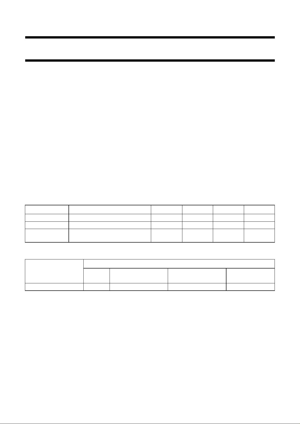
SYMBOL PARAMETER MIN. TYP. MAX. UNIT
V
DD
I
DD
T
amb
supply voltage 4.5 5.0 5.5 V
supply current − 50 − mA
operating ambient
0 − +70 °C
temperature
ORDERING INFORMATION
EXTENDED
TYPE NUMBER
PINS
PIN
POSITION
SAA4951WP 44 PLCC plastic SOT187
Note
1. SOT187-2; 1996 December 13.
April 1994 2
PACKAGE
MATERIAL CODE
(1)
Page 3
Philips Semiconductors Preliminary specification
Memory controller SAA4951
Y/U/V
BENDIC
SAA7158
12
NORIC
SAA4940
1212
MEMORY 1
1 × TMS4C2970
(3 × TMS4C1070)
VIDEO
REDUCTION
LINEFLICKER
ENHANCEMENT
NOISE
INCLUSIVE
REDUCTION
MEMORY 2
A/D
TDA8755
2
DACs
12
2
REDUCTION
CROSSCOLOUR
12
1 × TMS4C2970
(3 × TMS4C1070)
12
VCO2
12/13.5/16/18 MHz CONTROL 32/36 MHz
VCO1
H2, V2
(32 kHz/100 Hz)
SAA4951
MEMORY
CONTROLLER
2
27 MHz
VCO2B
µC-BUS
µC
28
MGH131
PCB83C652
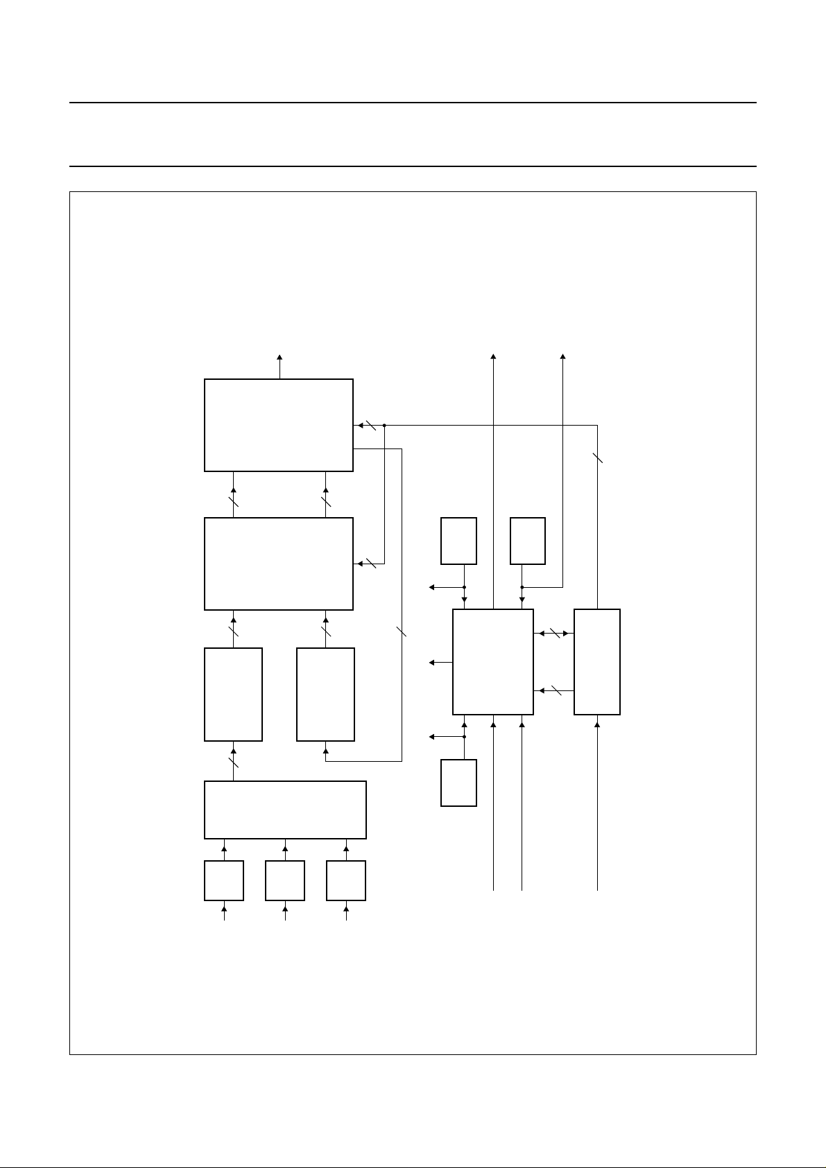
Fig.1 Improved Picture Quality (IPQ) module.
LPY
Y
handbook, full pagewidth
LPU
U
LPV
V
April 1994 3
SYNC
V
SCI
C
2
I
Page 4
Philips Semiconductors Preliminary specification
Memory controller SAA4951
PINNING
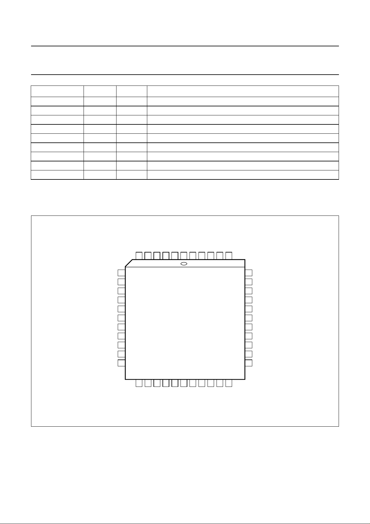
SYMBOL PIN TYPE
(1)
DESCRIPTION
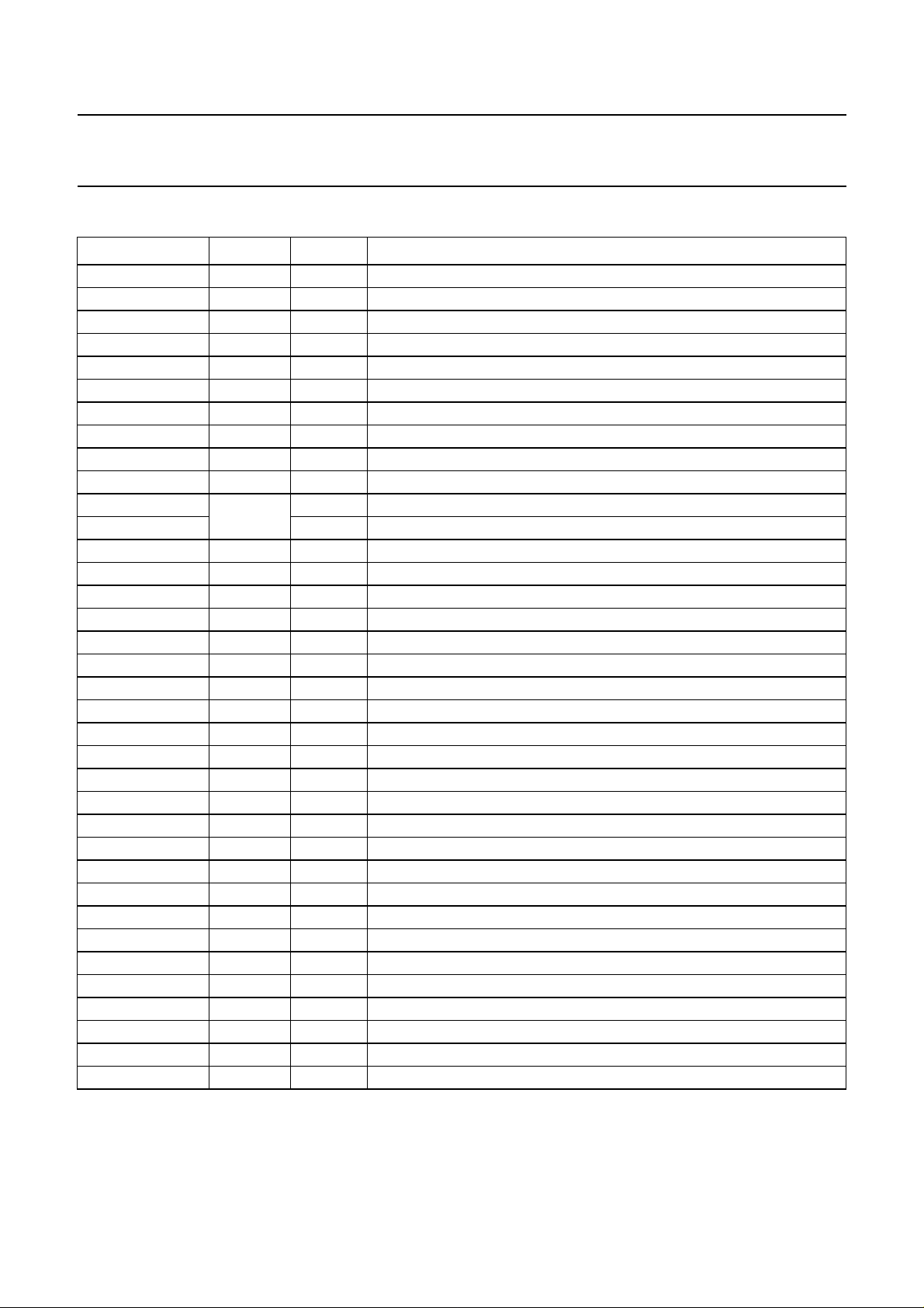
HRD 1 O horizontal reference signal, display part
V
DD
2 − positive supply voltage
SWC1 3 O serial write clock, memory 1
SRC 4 O serial read clock, memory 1
SWC2 5 O serial write clock, memory 2
WEXT 6 I external write enable input
IE1 7 O input enable signal, memory 1
WE1 8 O write enable signal, memory 1
STROBE 9 I strobe function
V
DD
10 − positive supply voltage
HRA 11 O horizontal reference signal, acquisition part
BLNA I horizontal blanking signal, acquisition part
V
SS
12 − ground
LLA 13 I line-locked clock signal, acquisition part
IE2 14 O input enable signal, memory 2
WE2 15 O write enable signal, memory 2
CLV 16 O video clamping signal
ALDUV/VB 17 O acquisition load signal, chrominance U, V / vertical blanking
RE1 18 O read enable signal, memory 1
RE2 19 O read enable signal, memory 2
BLND 20 O horizontal blanking signal, display part
ALE 21 I address latch enable signal
WRD 22 I write/read data signal
V
DD
V
SS
23 − positive supply voltage
24 − ground
P0 25 I data input signal, (LSB = least significant bit)
P1 26 I data input signal
P2 27 I data input signal
P3 28 I data input signal
P4 29 I data input signal
P5 30 I data input signal
P6 31 I/O data input/output signal
P7 32 I/O data input/output signal, (MSB = most significant bit)
LLDFL 33 I line-locked clock signal, deflection part
V
SS
34 − ground
HRDFL 35 O horizontal reference signal, deflection part
April 1994 4
Page 5
Philips Semiconductors Preliminary specification
Memory controller SAA4951
SYMBOL PIN TYPE
V
DD
36 − positive supply voltage
(1)
DESCRIPTION
HDFL 37 O horizontal synchronization signal, deflection part
VDFL 38 O vertical synchronization signal, deflection part
VACQ 39 I vertical synchronization signal, acquisition part
TEST 40 I test input
RSTW2 41 O reset write signal, memory 2
RSTW1 42 O reset write signal, memory 1
LLD 43 I line-locked clock signal, display part
V
SS
44 − ground
Note
1. I = Input
O = Output
handbook, full pagewidth
SS
WEXT
6
SWC2
5
SRC
4
SWC1
3
DD
V
2
HRD
1
LLD
V
44
43
RSTW1
RSTW2
42
41
TEST
40
IE1
WE1
STROBE
V
DD
HRA/BLNA
V
SS
LLA
IE2
WE2
CLV
ALDUV/VB
7
8
9
10
11
12
13
14
15
16
17
18
19
RE1
RE2
SAA4951WP
21
20
ALE
BLND
22
WRD
25
P0
26
P1
27
P2
23
24
SS
DD
V
V
28
P3
39
38
37
36
35
34
33
32
31
30
29
MGH129
VACQ
VDFL
HDFL
V
DD
HRDFL
V
SS
LLDFL
P7
P6
P5
P4
Fig.2 Pin configuration.
April 1994 5
Page 6

Philips Semiconductors Preliminary specification
Memory controller SAA4951
FUNCTIONAL DESCRIPTION
Block diagram and short description
The SAA4951 is a memory controller intended to be used
for scan conversion in TV receivers. This conversion is
done from 50 to 100 Hz or from 60 to 120 Hz. The device
supports three separate PLL circuits: the acquisition PLL
can run on 12, 13.5, 16 or 18 MHz, the display PLL on 27,
32 or 36 MHz, and the deflection PLL on 27 MHz. This
allows frequency doubling for input data rates of 13.5, 16
and 18 MHz. For displaying a 4:3 picture on a 16:9 screen
additional horizontal compression is possible when using
the clock configuration 12/32 MHz and 13.5/36 MHz. The
VCO and loop filter are peripheral parts of each PLL, the
clock divider and generation of the reference pulse for the
phase detector are internally provided.
The device generates all write, read and clock pulses to
operate a field memory in a desired mode. The required
signals are programmable via an 8-bit parallel
microcontroller port.
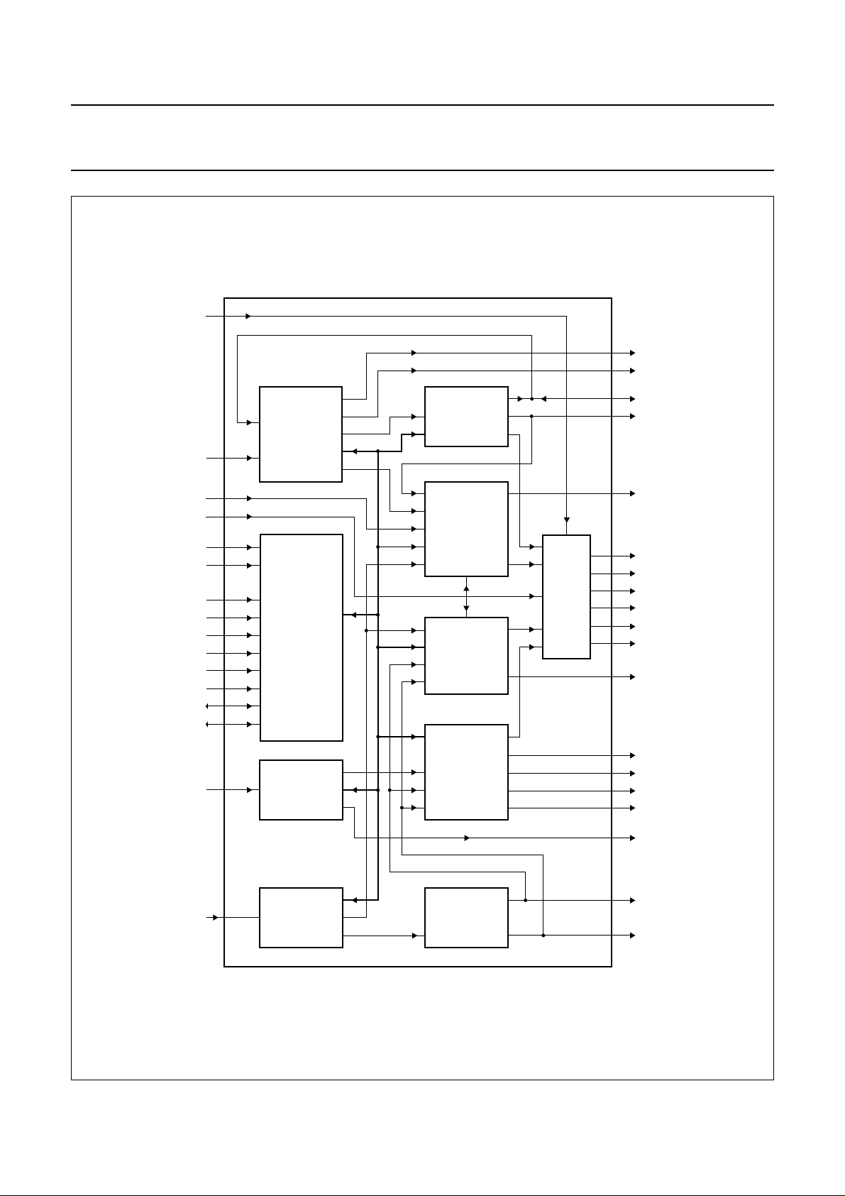
The block diagram of the SAA4951 is shown in Fig.3. The
clock signal from the VCO is fed in at pin 13, a horizontal
reference pulse for the phase discriminator is fed out at
pin 11.
By setting the clock divider to different values the PLL can
be forced to run on different clock frequencies.
Besides this the acquisition part can also be configured to
run on a fixed input clock. Then pin 11 is an input pin, so
the horizontal reference pulse can be supplied from the
outside. This mode is intended to be used together with a
digital decoder which is providing clock and reference
pulses.
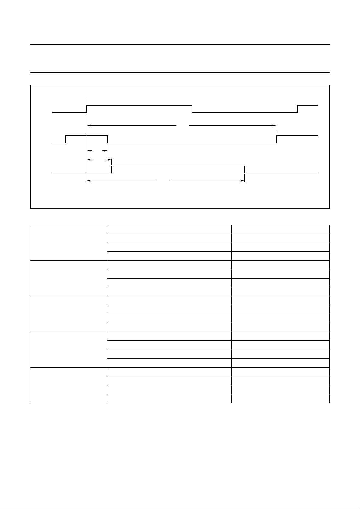
In the horizontal processing part the signals WE1, WE2
and CLV are generated. The vertical processing block
supplies the signals RSTW1 and RSTW2 as well as
enable signals for the horizontal part. The start and stop
position of the pulses are programmable, the increment
being 4 clock cycles in the horizontal part and 1 line in the
vertical part. For WE1 and WE2 an additional 2-bit fine
delay is available.
Display related control signals are derived from the display
PLL. The functions are similar to the acquisition part. The
PLL can be switched to 32 or 36 MHz, in case of 27 MHz
this clock is taken from the deflection PLL which always
runs on 27 MHz. In the horizontal part the pulse WE2,
RE1, RE2 and BLN are programmable in increments of 4
clock cycles, each one adjustable by an additional 2-bit
fine delay. The vertical processing block generates VDFL,
RSTW2 and enable signals for the horizontal part.
The deflection PLL runs on 27 MHz. From this clock the
16 kHz PLL reference pulse HRDFL is generated as well
as the 32 kHz deflection pulse HDFL.
In the vertical acquisition part the distance between the
incoming 50 Hz vertical synchronization pulse VACQ and
the horizontal synchronization pulse CLV generated by the
horizontal deflection circuit is measured. In addition the
field length is calculated by the acquisition counter, which
is enabled by CLV.
A fixed vertical reset pulse RSTW1 and a programmable
vertical control of the write enable pulse WE1 for
memory 1 defining the vertical write window are
generated.
In the display section the programmable 100 Hz write
enable pulse WE2 for the memory 2 and the
programmable 100 Hz read enable pulses RE1 and RE2
are provided. The 100 Hz vertical synchronizing signal
VDFL is corrected by the calculated values of the
acquisition part. The position of this pulse can also be
chosen by the microcontroller. Furthermore two field
identification signals for 50 Hz and for 100 Hz are
generated internally to mark the corresponding fields by
the microcontroller.
April 1994 6
Page 7
Philips Semiconductors Preliminary specification
Memory controller SAA4951
handbook, full pagewidth
WEXT
LLA
VACQ
STROBE
ALE
WRD
P0
P1
P2
P3
P4
P5
P6
P7
LLD
6
13
39
9
21
22
25
26
27
28
29
30
31
32
43
SAA4951
ACQ-CLOCK
GENERATOR
MICRO-
PROCESSOR-
INTERFACE
DSP-CLOCK
GENERATOR
ACQ
H-TIMING
ACQ
V-TIMING
DSP
V-TIMING
DSP
H-TIMING
LOGIC
17
ALDUV/VB
3
SWC1
11
HRA/BLNA
16
CLV
42
RSTW1
5
SWC2
41
RSTW2
8
WE1
15
WE2
7
IE1
14
IE2
38
VDFL
20
BLND
18
RE1
19
RE2
1
HRD
4
SRC
LLDFL
33
DFL-CLOCK
GENERATOR
Fig.3 Block diagram.
April 1994 7
DFL
TIMING
37
35
MGH130
HDFL
HRDFL
Page 8
Philips Semiconductors Preliminary specification
Memory controller SAA4951
Microcontroller interface
The SAA4951 is connected to a microcontroller via pins P0
to P7, ALE and WRD. This controller receives commands
from the I2C-bus and sets the registers of the
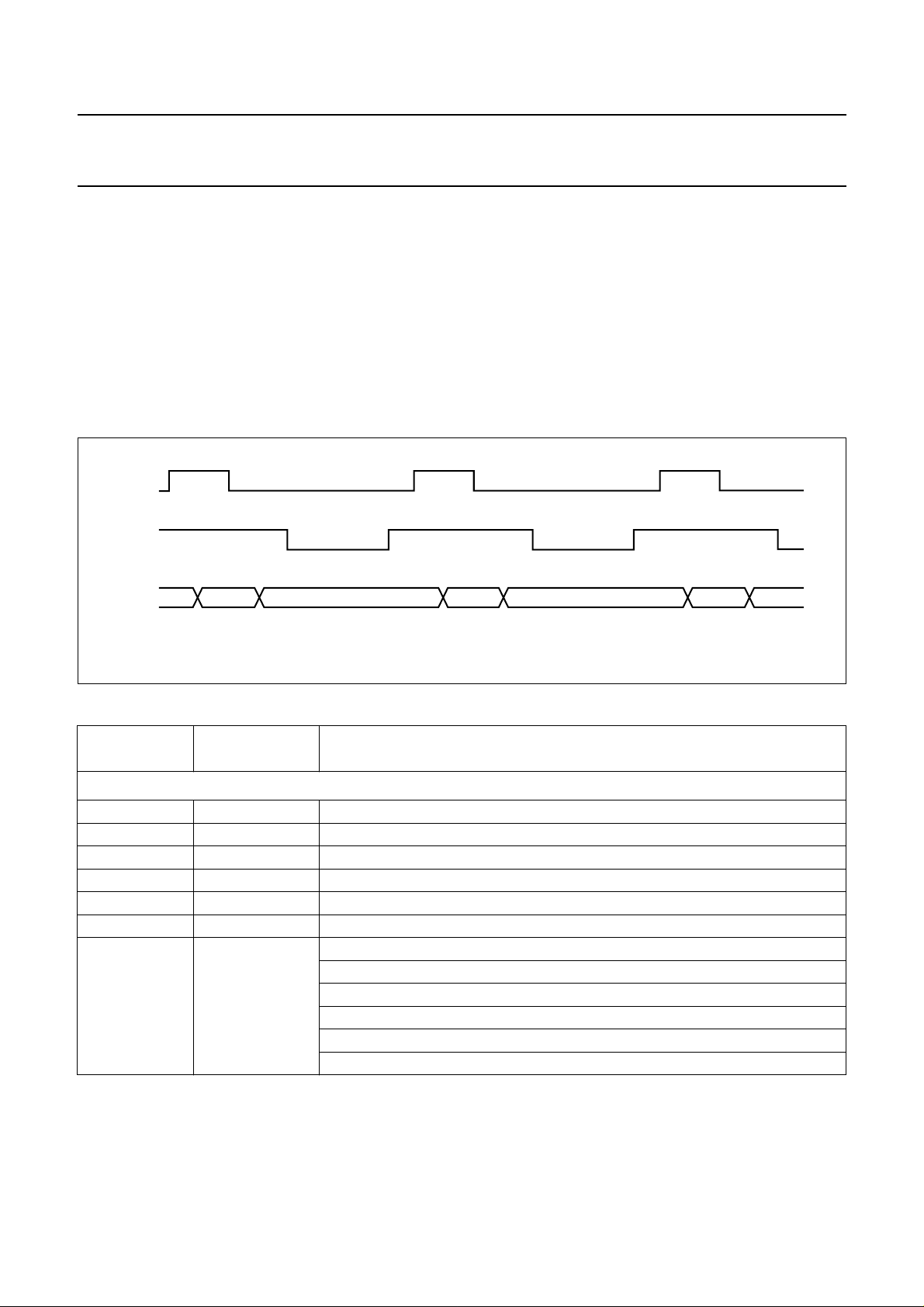
SAA4951 accordingly. Fig.4 shows the timing of these
signals. Address and data are transmitted sequentially on
the bus with the falling edge of ALE denoting a valid
address and the falling edge of WRD indicating valid data.
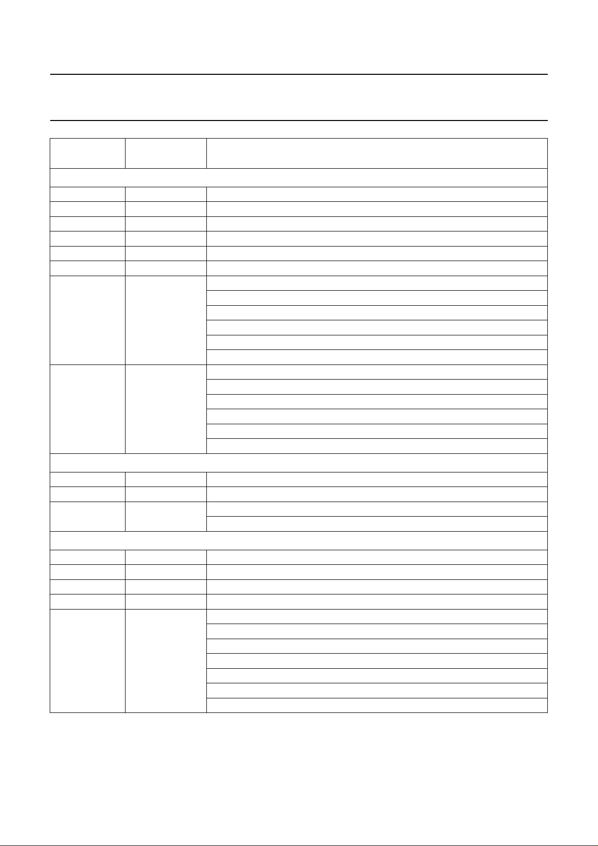
The individual registers, their address and their function
are listed in Table 1. Various start and stop registers are
handbook, full pagewidth
ALE
WRD
DATA
ADDRESS
DATA
Fig.4 µP-interface timing.
9 bits wide, in this case the MSB is combined with other
MSBs or fine delay control bits in an extra register which
has to be addressed and loaded separately.
In order to load the proper values to the vertical write
enable registers in case of median filtering, information
about the current 100 Hz field is necessary. To obtain
these data, the microcontroller sends the address 80Hex
(READ mode) which puts the SAA4951 in output mode for
the next address / data cycle. For this one cycle the WRD
pin works as a RDN pin.
ADDRESS
DATA
ADDRESS
MGH133
Table 1 Internal registers.
ADDRESS
(HEX)
REGISTER FUNCTION
Vertical pulses generated from the display clock
40 VDFLSTA start of VDFL pulse (lower 8 of 9 bits)
41 VDFLSTO end of VDFL pulse (lower 8 of 9 bits)
42 VWE2STA start of vertical write enable (lower 8 of 9 bits)
43 VWE2STO end of vertical write enable (lower 8 of 9 bits)
44 VRE2STA start of vertical read enable (lower 8 of 9 bits)
45 VRE2STO end of vertical write enable (lower 8 of 9 bits)
46 VDMSB bit 0: MSB of VDFLSTA
bit 1: MSB of VDFLSTO
bit 2: MSB of VWE2STA
bit 3: MSB of VWE2STO
bit 4: MSB of VRE1STA
bit 5: MSB of VRE1STO
April 1994 8
Page 9
Philips Semiconductors Preliminary specification
Memory controller SAA4951
ADDRESS
(HEX)
Horizontal pulses generated from the display clock
48 BLNDSTA start of horizontal blanking pulse (lower 8 of 9 bits)
49 BLNDSTO end of horizontal blanking pulse (lower 8 of 9 bits)
4A HWE2STA start of horizontal write enable (lower 8 of 9 bits)
4B HWE2STO end of horizontal write enable (lower 8 of 9 bits)
4C HRESTA start of horizontal read enable (lower 8 of 9 bits)
4D HRESTO end of horizontal read enable (lower 8 of 9 bits)
4E HDMSB bit 0: MSB of BLNDSTA
4F HDDEL bit 0: fine delay of BLND (LSB)
REGISTER FUNCTION
bit 1: MSB of BLNDSTO
bit 2: MSB of HWE2STA
bit 3: MSB of HWE2STO
bit 4: MSB of HRESTA
bit 5: MSB of HRESTO
bit 1: fine delay of BLND (MSB)
bit 2: fine delay of HWE2 (LSB)
bit 3: fine delay of HWE2 (MSB)
bit 4: fine delay of HRE (LSB)
bit 5: fine delay of HRE (MSB)
Vertical pulses generated from the acquisition clock
50 VWE1STA start of vertical write enable (lower 8 of 9 bits)
51 VWE1STO end of vertical write enable (lower 8 of 9 bits)
52 VAMSB bit 0: MSB of VWE1STA
bit 1: MSB of VWE1STO
Horizontal pulses generated from the acquisition clock
58 CLVSTA start of CLV pulse
59 CLVSTO end of CLV pulse
5A HWE1STA start of horizontal write enable (lower 8 of 9 bits)
5B HWE1STO end of horizontal write enable (lower 8 of 9 bits)
5C HAMSBDEL bit 0: MSB of HWE1STA
bit 1: MSB of HWE1STO
bit 2: fine delay of HWE1 (LSB)
bit 3: fine delay of HWE1 (MSB)
bit 4: memory configuration bit 2 (MC2): 0 = 1050/60; 1 = 1070/2970
bit 5: WEXT (external WE)
bit 6: SFR (select field recognition)
April 1994 9
Page 10
Philips Semiconductors Preliminary specification
Memory controller SAA4951
ADDRESS
(HEX)
Registers to turn on different modes
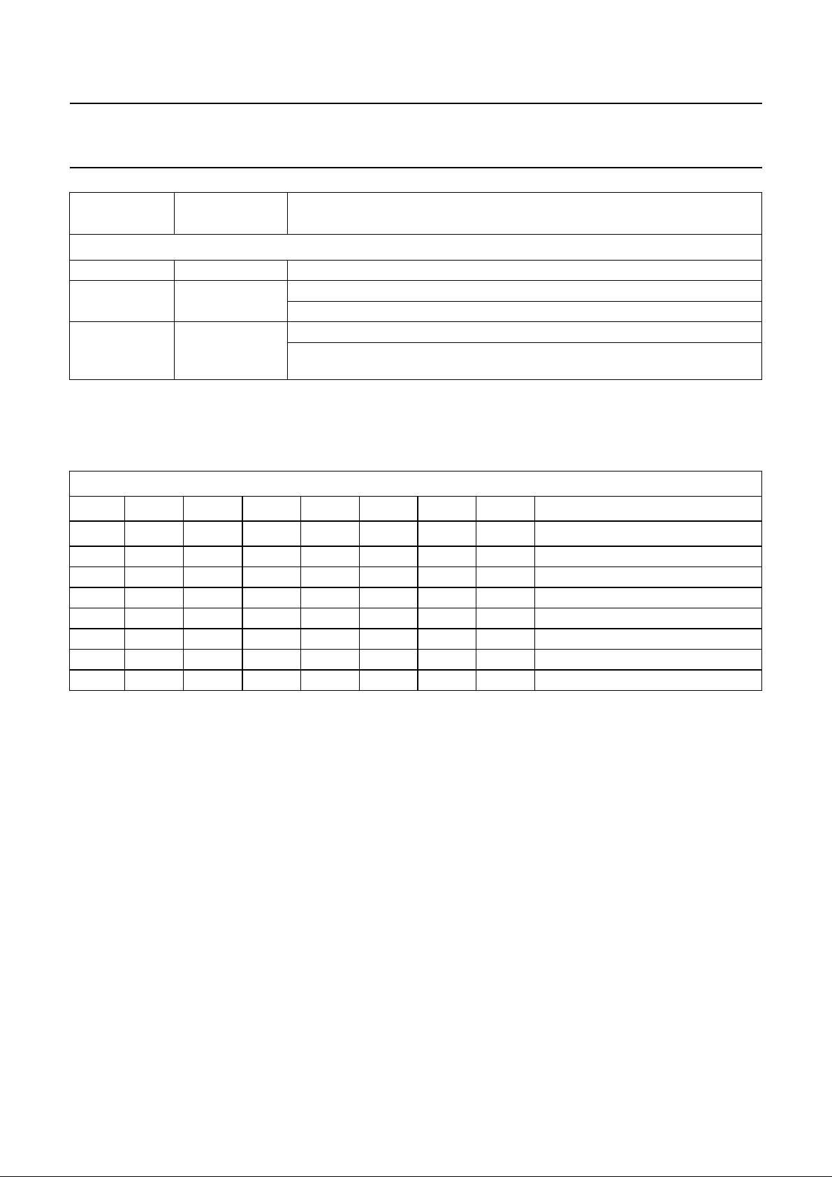
60 MODE0 mode register 0
61 MODE1 mode register 1
80 READ read mode
As it can be seen from the above table the registers form groups which are reflected in the addressing scheme according
to Table 2.
Table 2 Internal register addressing scheme.
RW OP MO AD HV D2 D1 D0
76543210
1XXXXXXXmicrocontroller reads data
00XXXXXXall registers off
011XXXXDselect mode 1 / mode 2
0 1 0 1 1 D D D select hor. ACQ registers
0 1 0 1 0 D D D select vert. ACQ registers
0 1 0 0 1 D D D select hor. DSP registers
0 1 0 0 0 D D D select vert. DSP registers
REGISTER FUNCTION
the bits of the two mode registers define the operating mode of the SAA4951
by sending this address the SAA4951 is switched to output mode for the next
address/data cycle, i. e. the microcontroller reads data from the SAA4951
INTERNAL REGISTER ADDRESS
Note
1. X = don’t care, D = data bit
bit names: RW read/write bit: 1 = read, 0 = write
OP operate bit, must be 1 to address any register
MO mode bit, select mode registers
AD select acquisition (= 1) or display (= 0) registers
HV select horizontal (= 1) or vertical (= 0) registers
D2 data bit 2
D1 data bit 1
D0 data bit 0
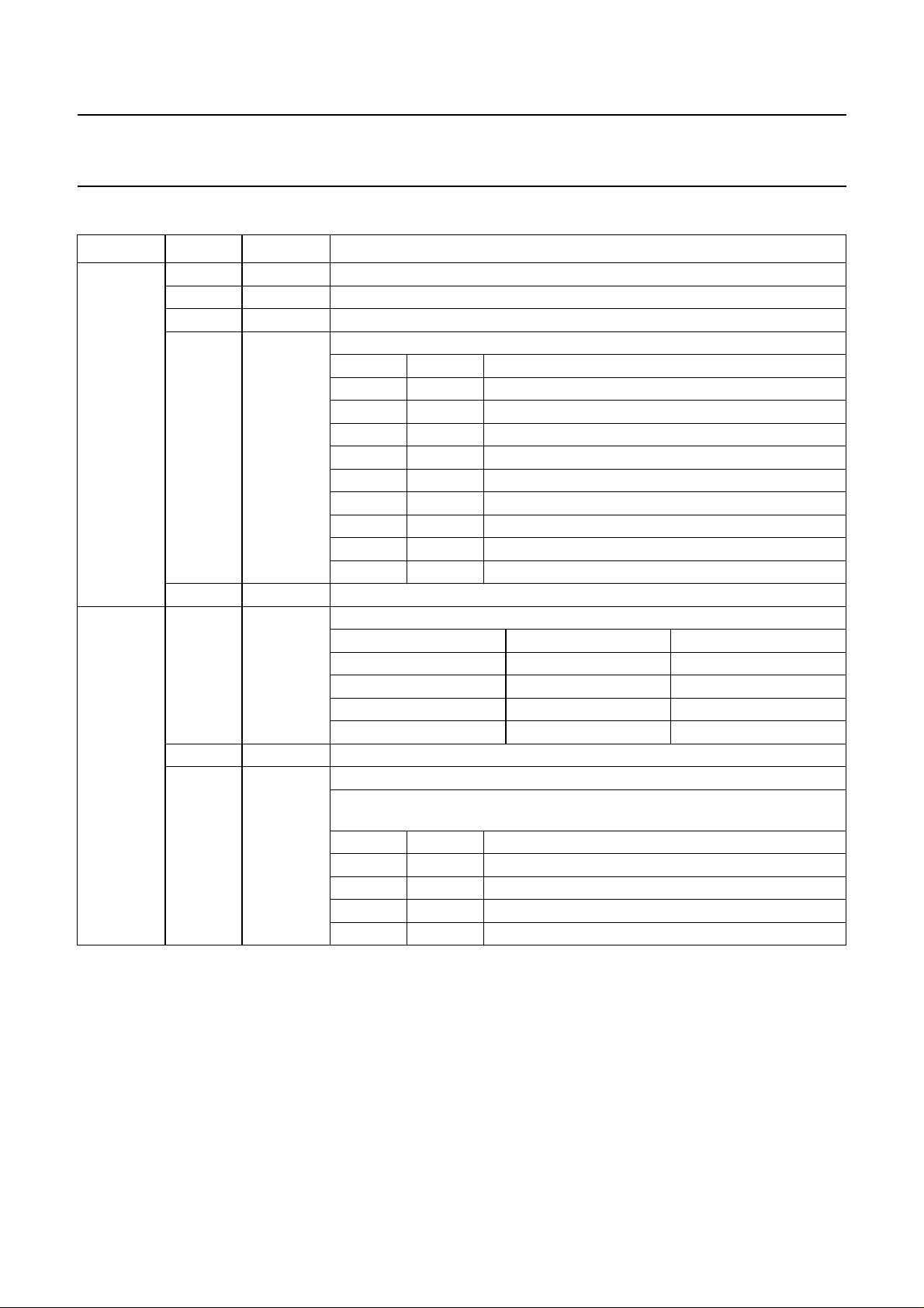
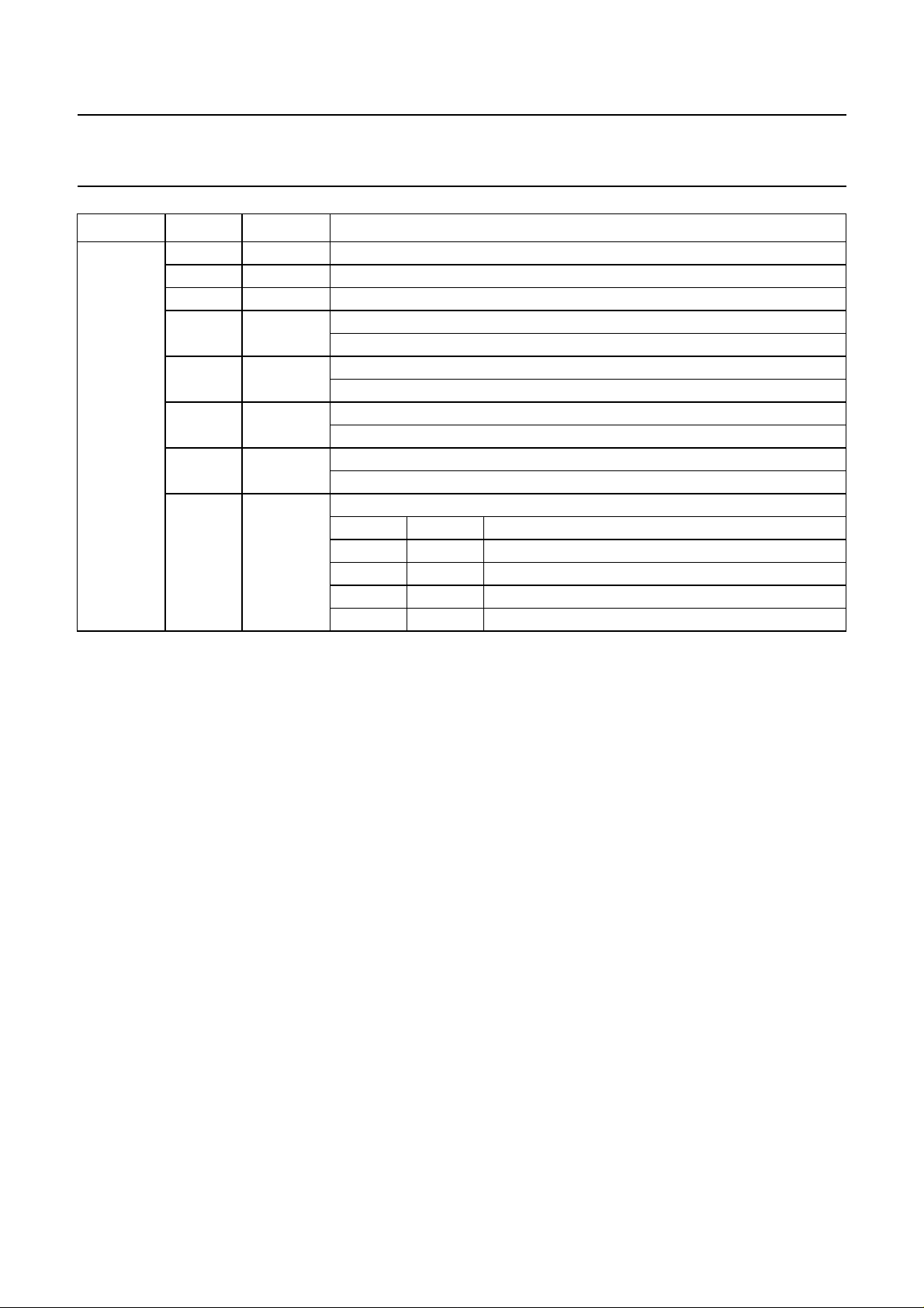
The bits of the two mode registers control the operation modes.
April 1994 10
Page 11
Philips Semiconductors Preliminary specification
Memory controller SAA4951
Table 3 Mode registers.
REGISTER BIT NAME REMARKS
MODE0 0 (LSB) FSA0 frequency select acquisition bit 0
1 FSA1 frequency select acquisition bit 1
2 FSD0 frequency select display bit 0
3 FSD1 frequency select display bit 1
FSA1 FSA0 acquisition frequency
0 0 12.0 MHz
0 1 13.5 MHz
1 0 16.0 MHz
1 1 18.0 MHz
FSD1 FSD0 display frequency
0 0 27.0 MHz
0 1 27.0 MHz
1 0 32.0 MHz
1 1 36.0 MHz
4 FORMAT0 control bit 0 for data format
MODE0 5 FORMAT1 control bit 1 for data format
FORMAT1 FORMAT0 Y:U:V data rate
0 0 4: 1: 1
0 1 4: 2: 2
1 0 4: 4: 4
1 1 4: 4: 4
6 HDEL0 horizontal delay control bit 0
7 (MSB) HDEL1 horizontal delay control bit 1
the bits HDEL0, HDEL1 control the position of the internal vertical read enable
signals for RE1
HDEL1 HDEL0
0 0 2 lines earlier
0 1 1 line earlier
1 0 normal
1 1 1 line later
April 1994 11
Page 12
Philips Semiconductors Preliminary specification
Memory controller SAA4951
REGISTER BIT NAME REMARKS
MODE1 0 (LSB) DR display raster
1 STPWM1 stop writing to memory 1: still picture mode
2 STPWM2 stop writing to memory 2: still picture mode
3 MC1 memory configuration bit 1
0: two field memories; 1: one field memory
4 GSC golden scart
0: normal IPQ mode; 1: golden scart input
5 CCIR60 for external mode (13.5 MHz input clock) only:
0 = 50 Hz, 864 clock cycles per line; 1 = 60 Hz, 858 clock cycles per line
6 EXTLLA horizontal reference pulse BLNA and clock LLA from external source
0: internal (PLL); 1: external
7 VFS vertical frequency select
VFS DR display mode
0 0 100 Hz (312.5 lines) ABAB raster
0 1 100 Hz (313/312.5/312/312.5 lines) AABB raster
1 0 50 Hz (625 lines) 1:1, non-interlaced
1 1 50 Hz (1250 lines) 2:1, interlaced
Description of acquisition part
LLA
This is the main input clock pulse for the acquisition side of
the memory controller generated by an external PLL
circuit. Depending on the chosen system application LLA
runs on the different frequencies of 12/13.5/16/18 MHz.
The PLL circuit is controlled by the analog burst key pulse
ABK provided by an inserted synchronization circuit (i. e.
TDA2579) and the horizontal reference signal HRA
supplied by the SAA4951 circuit.
WEXT
External write enable input for digital colour decoder
applications, where the write enable signal is generated by
the digital colour decoder. This signal is simply sampled by
LLA and fed out at WE1.
SWC1
The acquisition clock input signal LLA is connected
through the memory controller circuit. LLA is internally
buffered and put out as serial write clock SWC1 for the
memory 1. Additionally SWC1 is used as a clock signal for
the three AD-converters and for the formatter function.
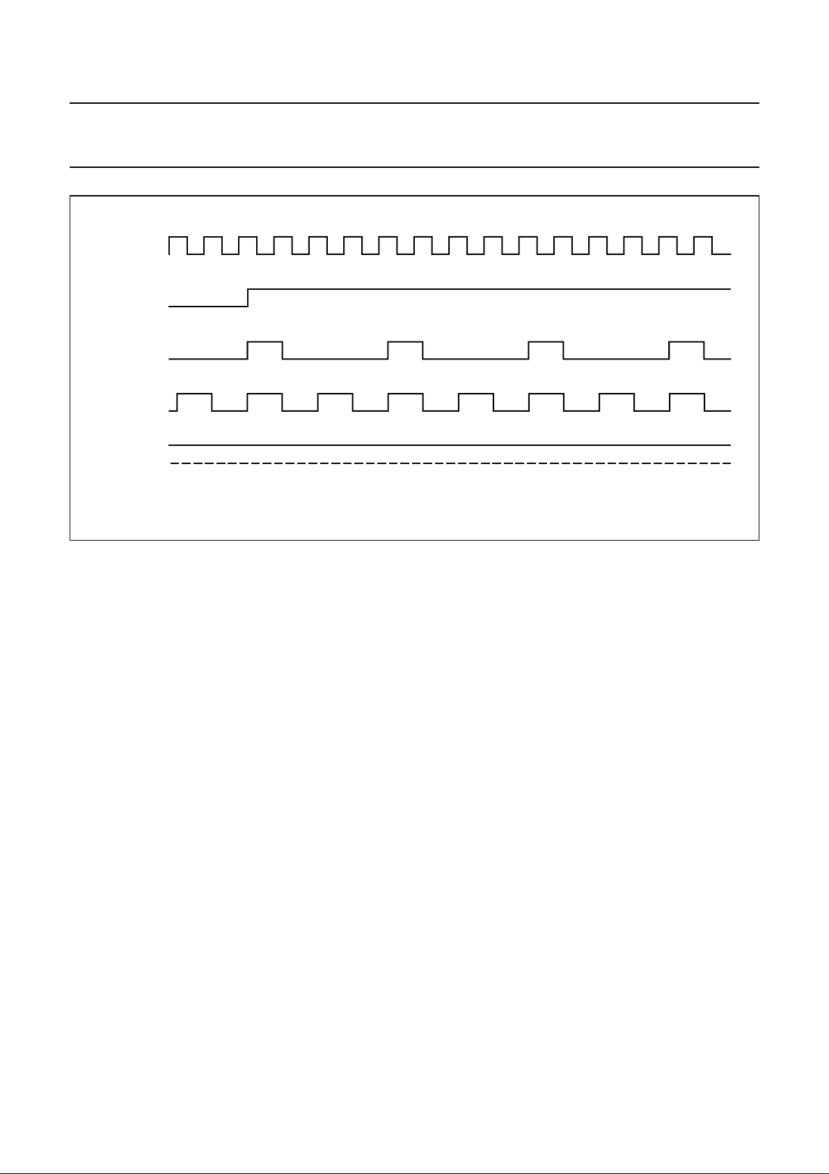
ALDUV/VB
The output signal ALDUV (analog load for the
chrominance signals U and V) controls the formation of the
8-bit digital data information of the chrominance signals U
and V.
April 1994 12
Page 13
Philips Semiconductors Preliminary specification
Memory controller SAA4951
handbook, full pagewidth
LLA
HRA
ALDUV
(format 4:1:1)
ALDUV
(format 4:2:2)
ALDUV
(format 4:4:4)
Fig.5 Timing of the signal ALDUV.
In case of an external write enable signal WEXT this output
provides a vertical blanking signal, which can be used to
generate a sandcastle pulse. The settings for the blanking
signal are done with the registers VWE1STA (falling edge)
and VWE1STO (rising edge).
CLV
The horizontal video clamping output pulse is generated
by the acquisition clock signal LLA and is used as clamp
pulse for the incoming luminance and chrominance signals
Y, U, V of the three analog to digital converters. The time
reference of CLV is the LOW-to-HIGH transition of the
HRA signal.
HRA/BLNA
The horizontal reference output pulse HRA operates on
the two standards PAL and NTSC.
In the PAL standard HRA has a frequency of 15.625 kHz
and in the NTSC standard the frequency is 15.734 kHz. In
both cases the duty cycle of this signal is 50%.
When the memory controller circuit is operating in a digital
environment, a horizontal reference signal BLNA and a
suitable acquisition clock pulse have to be supplied from
the external used circuits (i. e. SAA7151A, DMSD and
SAA7157, CGC).
MGH134
WE1
A HIGH level on this output pin enables picture data to be
written to field memory 1. WE1 is a composite signal,
which includes the horizontal write enable signal as well as
the vertical one.
It is possible to delay the horizontal timing of WE1 up to
three LLA clock cycles. In case of an external write enable
signal WEXT the horizontal and vertical settings and the
delay control have no influence on WE1.
WE1 operates at a vertical frequency of 50 Hz. When the
progressive scan mode is activated, WE1 is disabled
every second field. In still picture mode this signal is set to
LOW level.
IE1
This output signal is used as a data input enable for
memory 1. A logic HIGH level on this output pin enables
the data information to be written into field memory 1. Via
signal IE1 the still picture function is controlled. When this
mode is selected, IE1 is switched to LOW level. It is
possible to disable the still picture mode with externally
supplied STROBE pulses.
April 1994 13
Page 14
Philips Semiconductors Preliminary specification
Memory controller SAA4951
handbook, full pagewidth
HRA
CLV
r
CLV
CLV
f
WE1
r
WE1
WE1
f
Fig.6 Programmable horizontal acquisition signals.
Table 4 Horizontal programming range of CLV and WE1 (see also Fig.6).
13.5 MHz, 50 Hz CLV
13.5 MHz, 60 Hz CLV
18 MHz CLV
16 MHz CLV
12 MHz CLV
= (4Nr + 2) × LLA 0 ≤ Nr < 215
r
CLV
= (4Nf + 2) × LLA 0 < Nf ≤ 215
f
= (2Nr + 2) × LLA 0 ≤ Nr < 431
WE1
r
WE1
= (2Nf + 2) × LLA 0 < Nf ≤ 431
f
= (4Nr + 2) × LLA 0 ≤ Nr < 213
r
= (4Nf + 2) × LLA 0 < Nf ≤ 213
CLV
f
WE1
= (2Nr + 2) × LLA 0 ≤ Nr < 428
r
= (2Nf + 2) × LLA 0 < Nf ≤ 428
WE1
f
= (8Nr + 4) × LLA 0 ≤ Nr < 143
r
CLV
= (8Nf + 4) × LLA 0 < Nf ≤ 143
f
= (4Nr + 4) × LLA 0 ≤ Nr < 287
WE1
r
WE1
= (4Nf + 4) × LLA 0 < Nf ≤ 287
f
= (4Nr + 2) × LLA 0 ≤ Nr < 255
r
CLV
= (4Nf + 2) × LLA 0 < Nf ≤ 255
f
= (2Nr + 2) × LLA 0 ≤ Nr < 511
WE1
r
WE1
= (2Nf + 2) × LLA 0 < Nf ≤ 511
f
= (4Nr + 2) × LLA 0 ≤ Nr < 191
r
CLV
= (4Nf + 2) × LLA 0 < Nf ≤ 191
f
WE1
= (2Nr + 2) × LLA 0 ≤ Nr < 383
r
WE1
= (2Nf + 2) × LLA 0 < Nf ≤ 383
f
MGH135
Nr ≠ Nf
April 1994 14
Page 15
Philips Semiconductors Preliminary specification
Memory controller SAA4951
VACQ
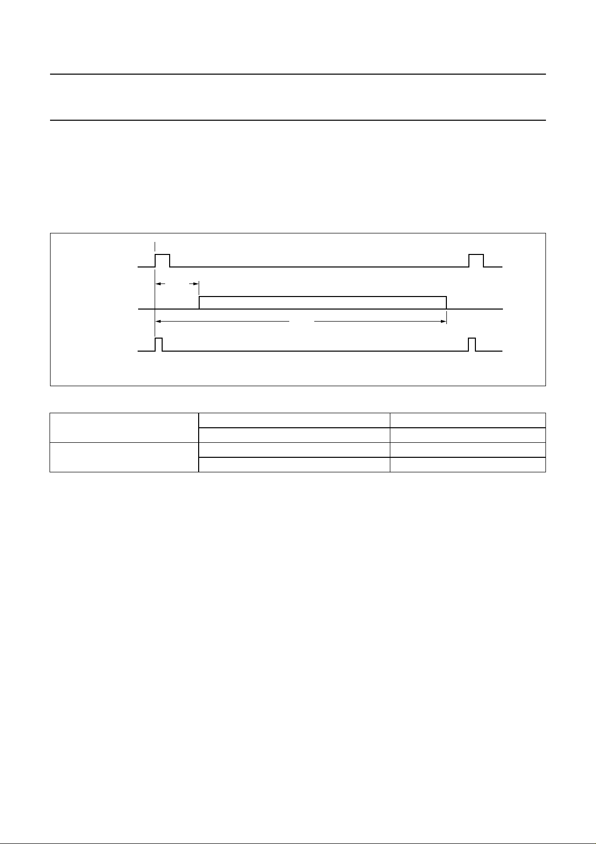
This is the 50 Hz vertical synchronization input signal
derived from a suitable vertical synchronization circuit (i. e.
TDA2579). The LOW-to-HIGH transition of this pulse is the
timing reference of all vertical control signals of the
SAA4951.
handbook, full pagewidth
VACQ
V
rWE1
WE1
V
fWE1
RSTW1
Fig.7 Vertical acquisition timing.
Table 5 Vertical programming range of WE1 (see also Fig.7).
50 Hz V
60 Hz V
=Nr×Line 1 ≤ Nr < 311
rWE1
V
= Nf × Line 1 < Nf ≤ 311
fWE1
=Nr×Line 1 ≤ Nr < 261
rWE1
= Nf × Line 1 < Nf ≤ 261
V
fWE1
RSTW1
The reset write output pulse 1 starts the write address
pointer of field memory 1. The RSTW1 signal is derived
from the 50 Hz vertical acquisition pulse VACQ and has a
pulse width of 64 µs (PAL) (see Fig.7).
MGH136
Nr ≠ Nf
STROBE
The asynchronous active HIGH STROBE input controls
the input enable signals IE1 and IE2 of the memory block
in the still picture mode.
Description of display part
LLD
The input signal LLD is the main line-locked clock for the
display side of SAA4951 generated by an external PLL
circuit. Depending on the chosen application, LLD runs on
three different frequencies 12/32/36 MHz. The PLL circuit
is controlled by the horizontal deflection drive output pulse
HDFL and the horizontal reference output signal HRD
supplied by the memory controller.
April 1994 15
SWC2
Depending on the chosen system mode the output pin
SWC2 delivers either the serial acquisition clock signal
LLA (PSC mode, 50 Hz) or the serial display clock pulse
LLD (two field memories, 100 Hz) to write the data
information into memory 2.
SRC
The display clock input signal LLD is connected through
the memory controller. LLD is internally buffered and put
out as serial read clock SRC for field memory 1.
Additionally SRC is used as clock pulse for the noise
reduction circuit NORIC and the backend circuit BENDIC.
HRD
The horizontal reference display pulse HRD has a duty
cycle of 50% and a frequency of 32 kHz. HRD is the
reference pulse for the horizontal timing of the control
signals RE1, RE2, WE2 and BLND generated by the
display circuit of SAA4951.
Page 16
Philips Semiconductors Preliminary specification
Memory controller SAA4951
BLND
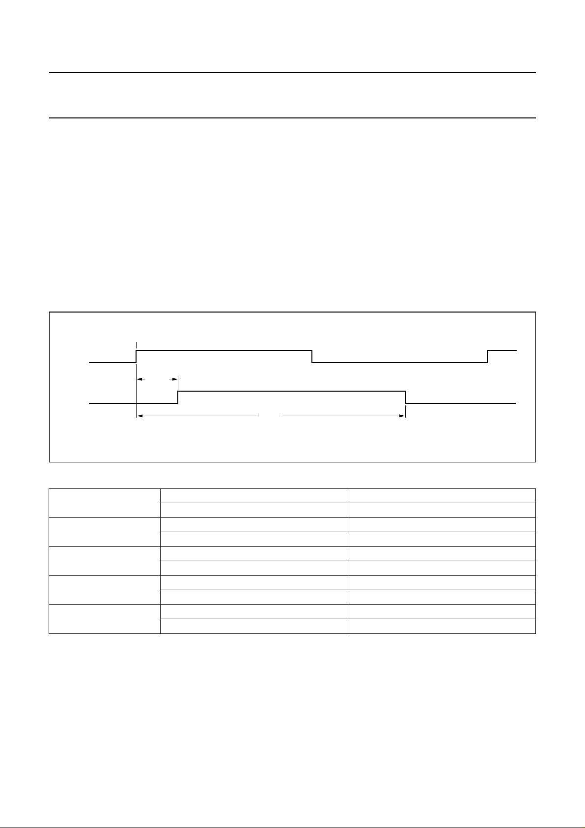
The output signal BLND is a horizontal blanking pulse and
is used for the peripheral circuits NORIC and BENDIC.
A LOW level indicates the blanking interval, a HIGH level
indicates valid data from the memories. It is possible to
delay the horizontal timing of BLND up to three steps of
LLD clock pulses.
handbook, full pagewidth
HRD
HDSP
r
HDSP
HDSP
WE2
A HIGH level on this output pin enables picture data to be
written to field memory 2. WE2 is a composite signal,
which includes the horizontal write enable signal as well as
the vertical one.
The horizontal timing of WE2 can be delayed up to three
steps of LLD clock pulses.
The WE2 output signal is used in different modes. When
two field memories are implemented in a serial structure,
WE2 operates at a vertical frequency of 100 Hz. In case
two field memories are connected in parallel, WE2 has a
vertical frequency of 50 Hz. In the progressive scan mode
the WE2 signal is disabled every second field.
f
MGH137
Fig.8 Programmable horizontal display signals (HDSP = BLN, WE2, RE1 or RE2).
Table 6 Horizontal programming range for display signals (HDSP = BLN, WE2, RE1 or RE2; see also Fig.8).
27 MHz, 50 Hz HDSP
HDSP
27 MHz, 60 Hz HDSP
HDSP
32 MHz HDSP
HDSP
36 MHz, 50 Hz HDSP
HDSP
36 MHz, 60 Hz HDSP
HDSP
= (2Nr + 2) × LLD 0 ≤ Nr < 431
r
= (2Nf + 2) × LLD 0 < Nf ≤ 431
f
= (2Nr + 2) × LLD 0 ≤ Nr < 428
r
= (2Nf + 2) × LLD 0 < Nf ≤ 428
f
= (2Nr + 2) × LLD 0 ≤ Nr < 511
r
= (2Nf + 2) × LLD 0 < Nf ≤ 511
f
= (4Nr + 4) × LLD 0 ≤ Nr < 287
r
= (4Nf + 4) × LLD 0 < Nf ≤ 287
f
= (4Nr + 4) × LLD 0 ≤ Nr < 285
r
= (4Nf + 4) × LLD 0 < Nf ≤ 285
f
Nr ≠ Nf
IE2
This output signal is used as data input enable for
memory 2. A logic HIGH level on this output pin enables
the data information to be written to field memory 2.
April 1994 16
Page 17
Philips Semiconductors Preliminary specification
Memory controller SAA4951
RE1
The output RE1 is the read enable signal for field
memory 1. A HIGH level enables the picture data to be
read from the memory. RE1 is a composite signal and
includes the horizontal read enable timing as well as the
vertical timing. It is possible to delay the horizontal timing
of RE1 up to three steps of LLD clock pulses.
Furthermore the vertical timing can be set one or two lines
before RE2 respectively one line after RE2 (median
filtering, noise reduction mode).
handbook, full pagewidth
VACQ
VDSP
r
VDSP
VDSP
f
RSTW2
RE2
The output RE2 is the read enable signal for field
memory 2. A HIGH level enables the picture data to be
read from memory 2. RE2 is a composite signal and
includes the horizontal read enable timing as well as the
vertical timing. The horizontal timing of RE2 can be
delayed up to three steps of LLD clock pulses.
MGH138
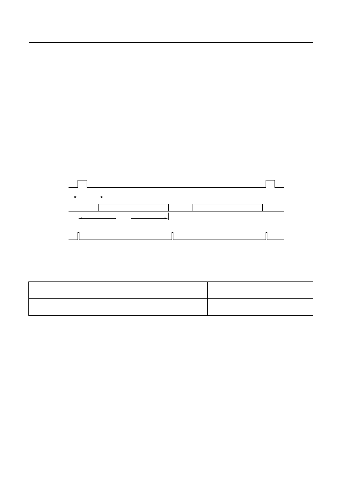
Fig.9 Vertical display timing (VDSP = V
WE2,VRE1/2
or VDFL).
Table 7 Vertical programming range for display signals (VDSP = WE2, RE1 or RE2; see also Fig.9).
50 Hz VDSP
VDSP
60 Hz VDSP
VDSP
= Nr × Line 1 ≤ Nr < 311
r
= Nf × Line 1 < Nf ≤ 311
f
= Nr × Line 1 ≤ Nr < 261
r
= Nf × Line 1 < Nf ≤ 261
f
Nr ≠ Nf
RSTW2
The reset write output pulse 2 starts the write address
pointer of field memory 2. There are two functions possible
for this pin. If a serial structure of the memories is
implemented, RSTW2 is a 100 Hz pulse; in progressive
scan mode and with one field memory, RSTW2 is a 50 Hz
pulse. The pulse duration of RSTW2 is 32 µs (PAL).
April 1994 17
Page 18
Philips Semiconductors Preliminary specification
Memory controller SAA4951
Description of deflection part
LLDFL
The input signal LLDFL is the main line-locked clock pulse
for the deflection side of the memory controller generated
by an external PLL circuit. The frequency of LLDFL is
always 27 MHz and is independent of the chosen feature
modes. The PLL circuit operates on the video clamping
pulse CLV of the acquisition part and the horizontal
reference signal HRDFL generated by the deflection side
of SAA4951.
handbook, full pagewidth
HRDFL
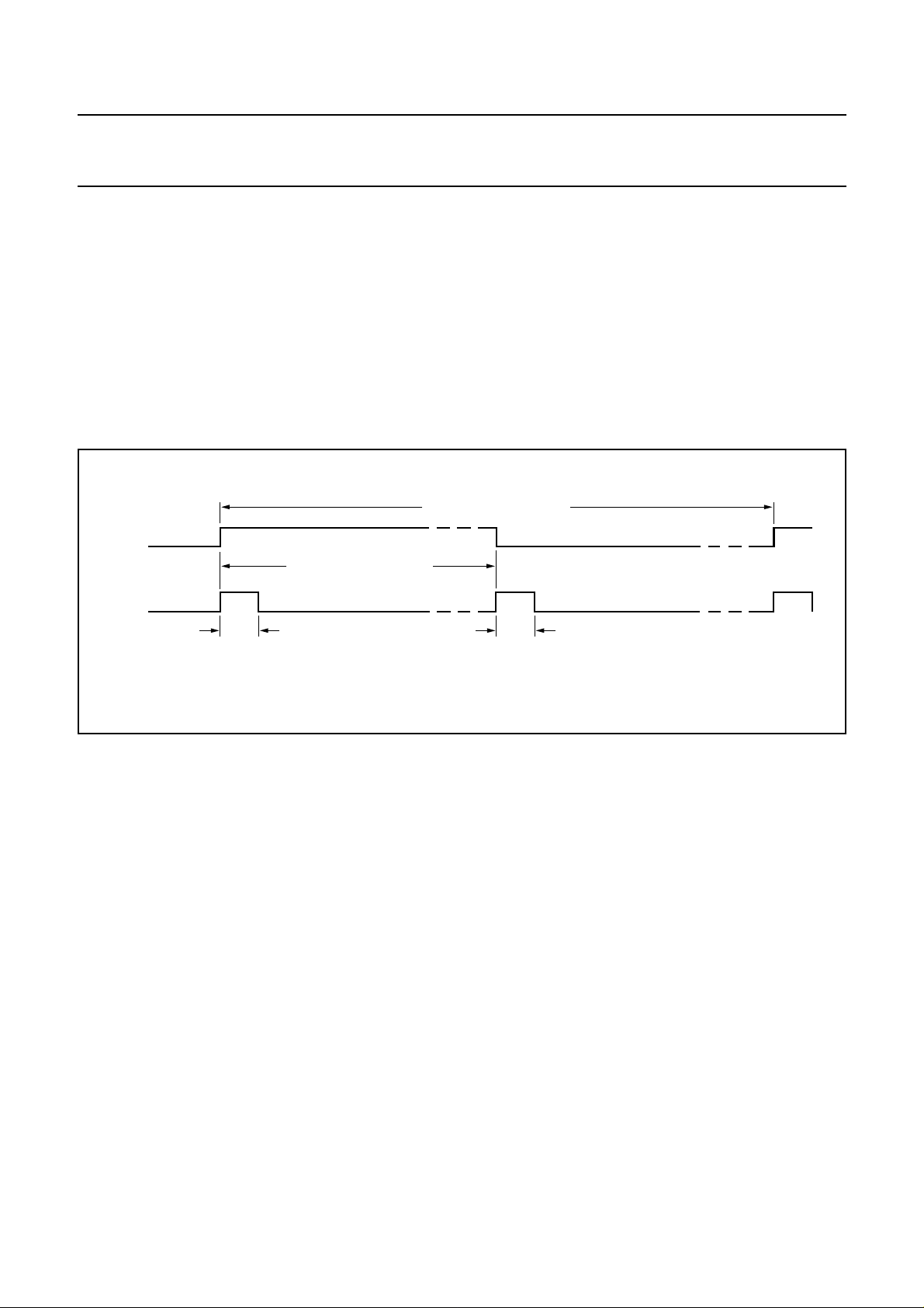
432/429 × LLDFL (50/60 Hz)
HDFL
64 × LLDFL 64 × LLDFL
864/858 × LLDFL (50/60 Hz)
HRDFL
This horizontal output signal is the reference pulse for the
horizontal deflection drive signal HDFL. The duty cycle of
HRDFL is 50% and the cycle time is 64 µs (PAL). In case
of golden scart mode the cycle time is reduced to 32 µs.
HDFL
The output signal HDFL is aimed for driving the connected
horizontal deflection circuit. HDFL has a cycle time of
32 µs and a pulse width of 64 x LLDFL = 2.37 µs
MGH139
Fig.10 Horizontal deflection timing.
VDFL
This is the vertical synchronization output signal generated
by the acquisition side of SAA4951. The timing reference
of VDFL is the LOW-to HIGH transition of the vertical
acquisition input pulse VACQ. Normally VDFL has a pulse
width of 2.5 x HDFL = 80 µs and a cycle time of 100 Hz.
In normal mode the memory controller operates with two
field memories and 100 Hz interlace picture reproduction.
When the system includes only one field memory it is
necessary to activate the AABB mode. In the simple field
repetition mode the first two and the last two 100 Hz fields
are out one upon another
Description of control inputs/outputs
ALE
The address latch enable input signal ALE is provided by
the microcontroller. A falling edge of ALE denotes a valid
address.
WRD
This is the write/read enable control signal supplied by the
microcontroller. The HIGH-to-LOW transition of WRD
indicates valid data.
P0 to P7
The SAA4951 is controlled by the bidirectional port bus
P0.0 to P0.7 of a microcontroller. Address and data are
transmitted sequentially on the bus.
TEST
The TEST input pin has to be connected to ground.
April 1994 18
Page 19
Philips Semiconductors Preliminary specification
Memory controller SAA4951
Timing specification
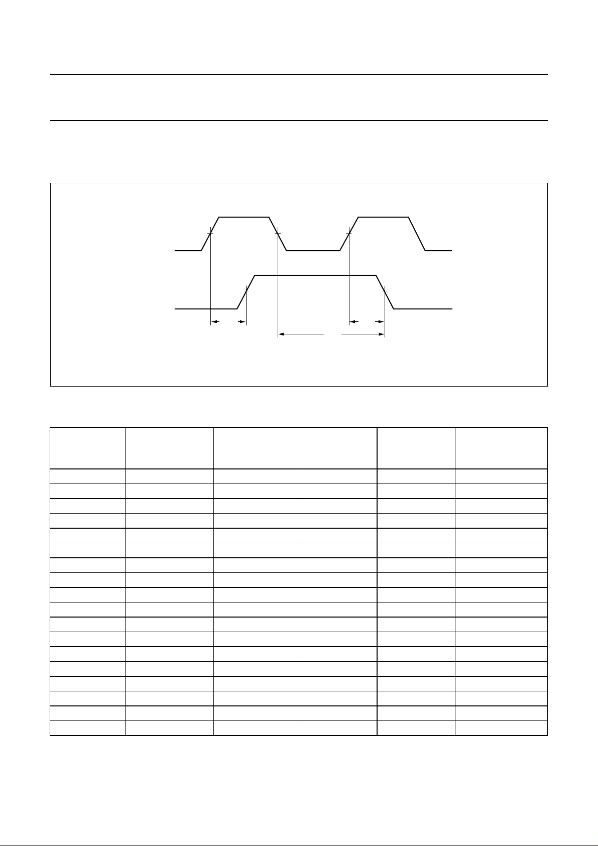
The internal delays of the output signals referred to the respective clock are given in Table 8.
handbook, full pagewidth
CLK
OUT
t
PLH
t
PD
t
PHL
MGH140
Fig.11 Timing diagram.
Table 8 Delay table.
Conditions: V
CLK OUT
= +4.5 V; Tj=+70 °C (worst case).
DD
LOAD
(pF)
t
PLH
(ns)
t
PHL
(ns)
LLA SWC1 15 6.4 − 6.5
LLD SRC 45 11.2 − 13.7
LLDFL SRC 45 11.9 − 13.9
SRC SWC2 25 3.2 − 2.6
SWC1 WE1 15 15.9 18.9 −
SWC2 WE2 10 8.0 10.9 −
SRC RE1 10 7.0 8.6 −
SRC RE2 10 7.2 8.7 −
LLDFL HDFL 25 12.8 15.8 −
LLDFL HRDFL 10 11.9 13.9 −
SWC1 HRA 10 6.5 8.4 −
SRC HRD 10 5.6 7.6 −
SRC BLND 25 7.4 10.3 −
SWC1 ALDUV 25 11.5 14.0 −
LLDFL VB 25 28.2 30.3 −
SWC1 CLV 25 8.3 11.3 −
LLDFL VDFL 25 24.6 27.6 −
LLA WE1(EXT) 25 18.1 21.1 −
t
PD
(ns)
April 1994 19
Page 20
Philips Semiconductors Preliminary specification
Memory controller SAA4951
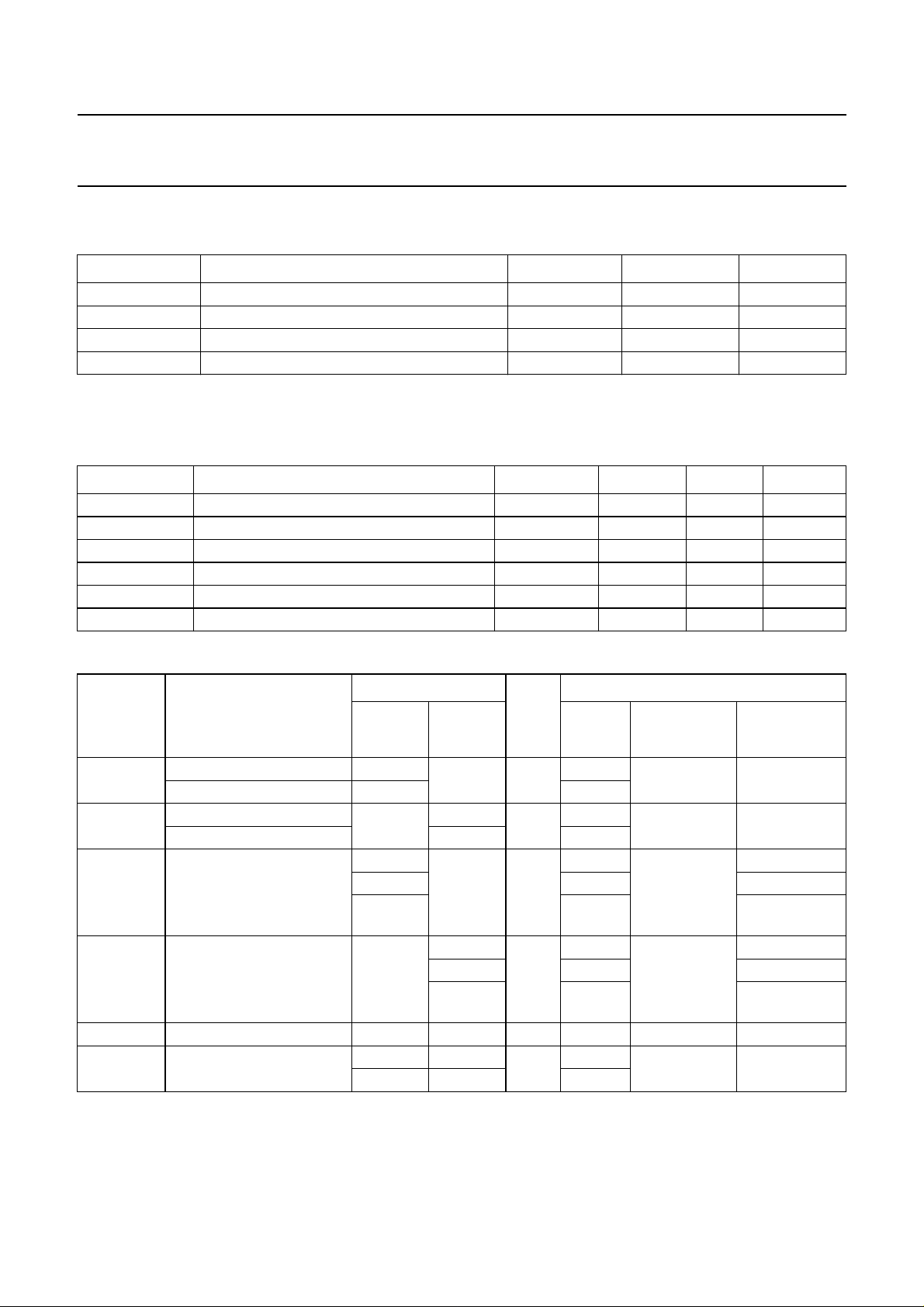
LIMITING VALUES
In accordance with the Absolute Maximum Rating System (IEC 134).
SYMBOL PARAMETER MIN. MAX. UNIT
V
DD
V
I
T
amb
T
stg
CHARACTERISTICS
Recommended operating conditions
SYMBOL PARAMETER MIN. TYP. MAX. UNIT
V
DD
V
I
V
O
I
DD
T
amb
T
j
supply voltage −0.5 +6.0 V
input voltage −0.5 VDD+ 0.5 V
operating ambient temperature 0 +70 °C
storage temperature −40 +125 °C
DC supply voltage 4.5 5.0 5.5 V
DC input voltage −0.5 − VDD+0.5 V
DC output voltage −0.5 − VDD+0.5 V
supply current − 50 − mA
operating ambient temperature 0 − 70 °C
junction temperature 0 − 140 °C
DC Characteristics
SYMBOL PARAMETER
v
IH
TTL-input 2.0 − V 4.5 −−
HIGH level input voltage 2.0 5.5
V
IL
TTL-input − 0.8 V 4.5 −−
LOW level input voltage 0.8 5.5
V
OH
V
OL
I
LI
R
pull
HIGH level output voltage 4.4 − V 4.5 VIHor V
LOW level output voltage − 0.1 V 4.5 VIH or V
input leakage current −±1.0 µA 5.5 VDDor V
internal pull-up resistor
for I/O cells
T
= +25 °C
amb
MIN. MAX.
UNIT
V
TEST CONDITIONS
DD
V
I
OTHER
(V) (V)
IL
5.4 5.5 I
3.1 4.5 I
I0= −2 µA
= −2 µA
0
= −4.0 mA/
0
8.0 mA (SRC)
IL
0.1 5.5 I
0.27 4.5 I
I0= +2 µA
= +2 µA
0
= −4.0 mA/
0
8.0 mA (SRC)
SS
−
42 150 kΩ 4.5 −−
35 105 5.5
April 1994 20
Page 21

Philips Semiconductors Preliminary specification
Memory controller SAA4951
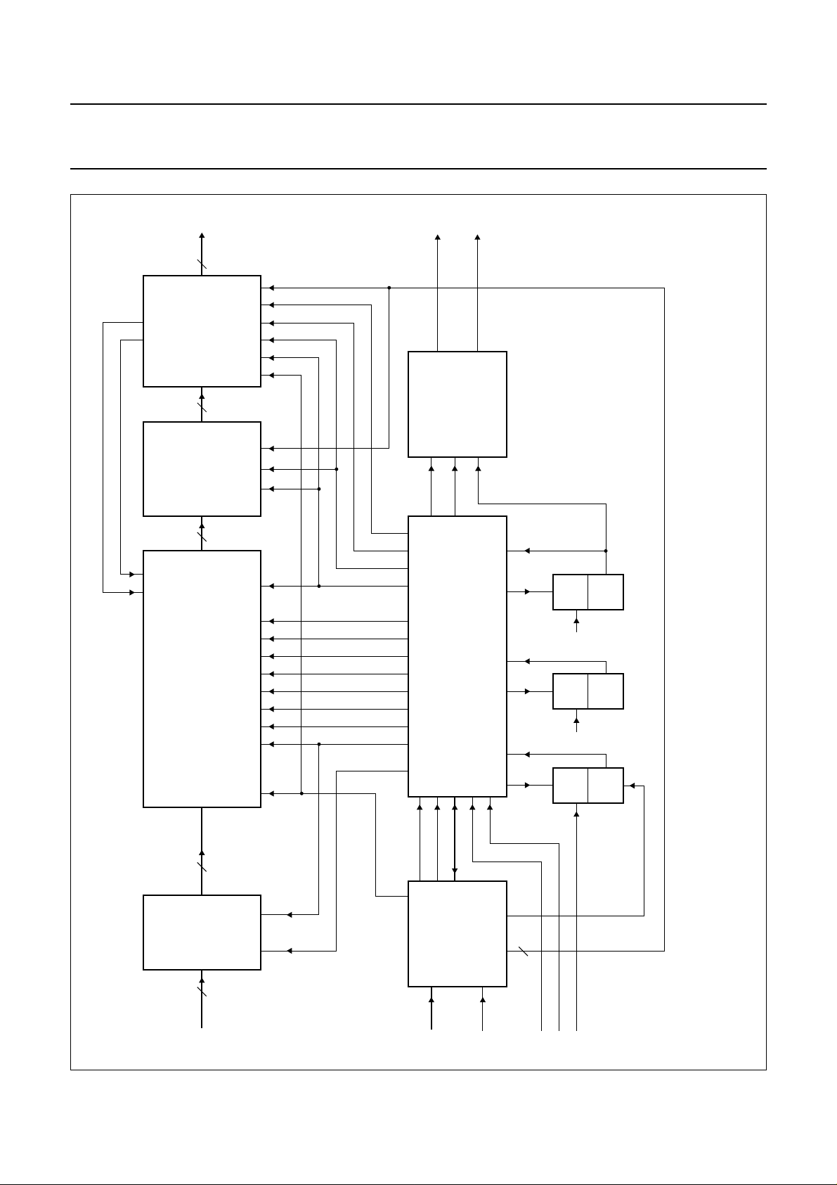
APPLICATION INFORMATION
Fig.12 shows a block diagram of the application environment of the memory controller SAA4951. The full option chip set
2
of the new TV-feature system (third generation) controlled by the I
TDA8709 3× ADC (8-bit) with clamp and gain setting, 30 MHz or
TDA8755 1× ADC
TMS4C10XX 1 Mbit video RAM, (optional TMS4C1050/60/70) or
TMS4C2970 2.9 Mbit video RAM
SAA7158 BENDIC (Back END IC) with LFR, CTI, Y-Peaking, DAC
SAA4940 NORIC (NOise Reduction IC) with Noise Reduction (NR) and Cross Colour Reduction (CCR)
SAA4951 Memory controller
83C652 µC software control of activated features
C-bus includes the following circuits:
April 1994 21
Page 22
Philips Semiconductors Preliminary specification
Memory controller SAA4951
V
H
DEFLECTION
LLDFL
27 MHz
HDFL
38
37
SAA4951
143 35 33
MEMORY CONTROLLER
LLA
PD
CLVHDFL
32/36 MHz 27 MHz
PD
12/13.5/16/
18 MHz
MGH132
VCO
VCO
Fig.12 Application diagram.
ook, full pagewidth
(1)
RE2
(1)
RE1
Y/U/V
VIDEO
BENDIC
SAA7158
ENHANCEMENT
24
NOISE
NORIC
SAA4940
REDUCTION
24 3
MEMORY BLOCK
DACs
REDUCTION
LINEFLICKER
INCLUSIVE
REDUCTION
CROSSCOLOUR
or
2 × TMS4C2970
6 × TMS4C1050/60/70
VDFL
RE2
RE1
BLND
SRC
RSTW2
SWC2
WE2
IE2
RSTW1
WE1
IE1
SWC1
CLV
RSTR
ADC
12
Y/U/V
TDA8755
3
SWC1
(1)
CLV
April 1994 22
16 3 7 8 42 14 15 5 41 1942018
21
ALE
C
2
I
WRD
22
25 to 32939
P0 to P7
STROBE
83C652
MICRO-
CONTROLLER
VDFL
11 13
VACQ
HRA HRD HRDFL LLDFLLLD
2
VACQ
STROBE
PD
ABK
VCO
COMP
MICROCONTROLLER-BUS
former: 3 x TDA8709 + external formatter
(1)
Page 23
Philips Semiconductors Preliminary specification
Memory controller SAA4951
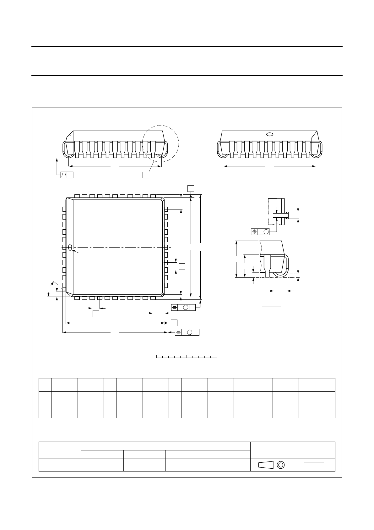
PACKAGE OUTLINE
PLCC44: plastic leaded chip carrier; 44 leads
e
D
y
40
44
1
pin 1 index
6
β
k
717
e
D
H
D
X
2939
SOT187-2
e
E
A
Z
E
28
H
E
E
A
A
1
A
e
18
k
1
v M
Z
D
A
4
B
v M
B
w M
detail X
b
p
b
1
(A )
3
L
p
0 5 10 mm
scale
DIMENSIONS (millimetre dimensions are derived from the original inch dimensions)
UNIT A
mm
inches
A
1
min. max. max. max. max.
4.57
0.51
4.19
0.180
0.020
0.165
A
0.25
0.01
A
4
3
3.05
0.12
b
0.53
0.33
0.021
0.013
b
p
1
0.81
0.66
0.032
0.026
D
16.66
16.51
0.656
0.650
(1)
(1)
E
eH
16.66
1.27
16.51
0.656
0.05
0.650
e
16.00
14.99
0.630
0.590
e
E
D
17.65
16.00
17.40
14.99
0.695
0.630
0.685
0.590
Note
1. Plastic or metal protrusions of 0.01 inches maximum per side are not included.
OUTLINE
VERSION
SOT187-2
IEC JEDEC EIAJ
112E10 MO-047AC
REFERENCES
April 1994 23
H
E
D
17.65
17.40
0.695
0.685
k
1.22
1.07
0.048
0.042
k
0.51
0.020
1
0.057
0.040
L
p
1.44
1.02
EUROPEAN
PROJECTION
(1) (1)
Z
Z
E
D
ywv β
0.18 0.100.18
0.007 0.0040.007
2.16
0.085
2.16
0.085
o
45
ISSUE DATE
92-11-17
95-02-25
Page 24

Philips Semiconductors Preliminary specification
Memory controller SAA4951
SOLDERING
Introduction
There is no soldering method that is ideal for all IC
packages. Wave soldering is often preferred when
through-hole and surface mounted components are mixed
on one printed-circuit board. However, wave soldering is
not always suitable for surface mounted ICs, or for
printed-circuits with high population densities. In these
situations reflow soldering is often used.
This text gives a very brief insight to a complex technology.
A more in-depth account of soldering ICs can be found in
“IC Package Databook”
our
Reflow soldering
Reflow soldering techniques are suitable for all PLCC
packages.
The choice of heating method may be influenced by larger
PLCC packages (44 leads, or more). If infrared or vapour
phase heating is used and the large packages are not
absolutely dry (less than 0.1% moisture content by
weight), vaporization of the small amount of moisture in
them can cause cracking of the plastic body. For more
information, refer to the Drypack chapter in our
Reference Handbook”
Reflow soldering requires solder paste (a suspension of
fine solder particles, flux and binding agent) to be applied
to the printed-circuit board by screen printing, stencilling or
pressure-syringe dispensing before package placement.
Several techniques exist for reflowing; for example,
thermal conduction by heated belt. Dwell times vary
between 50 and 300 seconds depending on heating
method. Typical reflow temperatures range from
215 to 250 °C.
(order code 9398 652 90011).
“Quality
(order code 9397 750 00192).
Wave soldering
Wave soldering techniques can be used for all PLCC
packages if the following conditions are observed:
• A double-wave (a turbulent wave with high upward
pressure followed by a smooth laminar wave) soldering
technique should be used.
• The longitudinal axis of the package footprint must be
parallel to the solder flow.
• The package footprint must incorporate solder thieves at
the downstream corners.
During placement and before soldering, the package must
be fixed with a droplet of adhesive. The adhesive can be
applied by screen printing, pin transfer or syringe
dispensing. The package can be soldered after the
adhesive is cured.
Maximum permissible solder temperature is 260 °C, and
maximum duration of package immersion in solder is
10 seconds, if cooled to less than 150 °C within
6 seconds. Typical dwell time is 4 seconds at 250 °C.
A mildly-activated flux will eliminate the need for removal
of corrosive residues in most applications.
Repairing soldered joints
Fix the component by first soldering two diagonallyopposite end leads. Use only a low voltage soldering iron
(less than 24 V) applied to the flat part of the lead. Contact
time must be limited to 10 seconds at up to 300 °C. When
using a dedicated tool, all other leads can be soldered in
one operation within 2 to 5 seconds between
270 and 320 °C.
Preheating is necessary to dry the paste and evaporate
the binding agent. Preheating duration: 45 minutes at
45 °C.
April 1994 24
Page 25
Philips Semiconductors Preliminary specification
Memory controller SAA4951
DEFINITIONS
Data sheet status
Objective specification This data sheet contains target or goal specifications for product development.
Preliminary specification This data sheet contains preliminary data; supplementary data may be published later.
Product specification This data sheet contains final product specifications.
Limiting values
Limiting values given are in accordance with the Absolute Maximum Rating System (IEC 134). Stress above one or
more of the limiting values may cause permanent damage to the device. These are stress ratings only and operation
of the device at these or at any other conditions above those given in the Characteristics sections of the specification
is not implied. Exposure to limiting values for extended periods may affect device reliability.
Application information
Where application information is given, it is advisory and does not form part of the specification.
LIFE SUPPORT APPLICATIONS
These products are not designed for use in life support appliances, devices, or systems where malfunction of these
products can reasonably be expected to result in personal injury. Philips customers using or selling these products for
use in such applications do so at their own risk and agree to fully indemnify Philips for any damages resulting from such
improper use or sale.
April 1994 25
 Loading...