

Page 1

INTEGRATED CIRCUITS
DATA SH EET
SAA3008
Infrared remote control transmitter
(RECS 80 low voltage)
Preliminary specification
File under Integrated Circuits, IC02
December 1988
Page 2

Philips Semiconductors Preliminary specification
Infrared remote control transmitter
SAA3008
(RECS 80 low voltage)
GENERAL DESCRIPTION
The SAA3008 transmitter IC is designed for infrared remote control systems. It has a capacity for 1280 commands
arranged in 20 sub-system address groups of 64 commands each. The subsystem address may be selected by
press-button, slider switches or be hard-wired.
Commands are transmitted in patterns which are pulse distance coded. Modulated pulse transmissions allow a
narrow-band receiver to be used for improved noise rejection. The modulation frequency of the SAA3008 is 38 kHz which
is1⁄12 of the oscillator frequency of 455 kHz (typical).
Features
• Modulated transmission
• Ceramic resonator controlled frequency
• Data-word-start with reference time of unique start pattern
• Supply voltage range 2 V to 6.5 V
• 40 mA output current capability
• Very low standby current (< 4 µA at V
• Up to 20 subsystem address groups; up to 1280 commands
• Up to 64 commands per subsystem address; up to 1280 commands
• Requires few additional components
DD
= 6 V)
PACKAGE OUTLINES
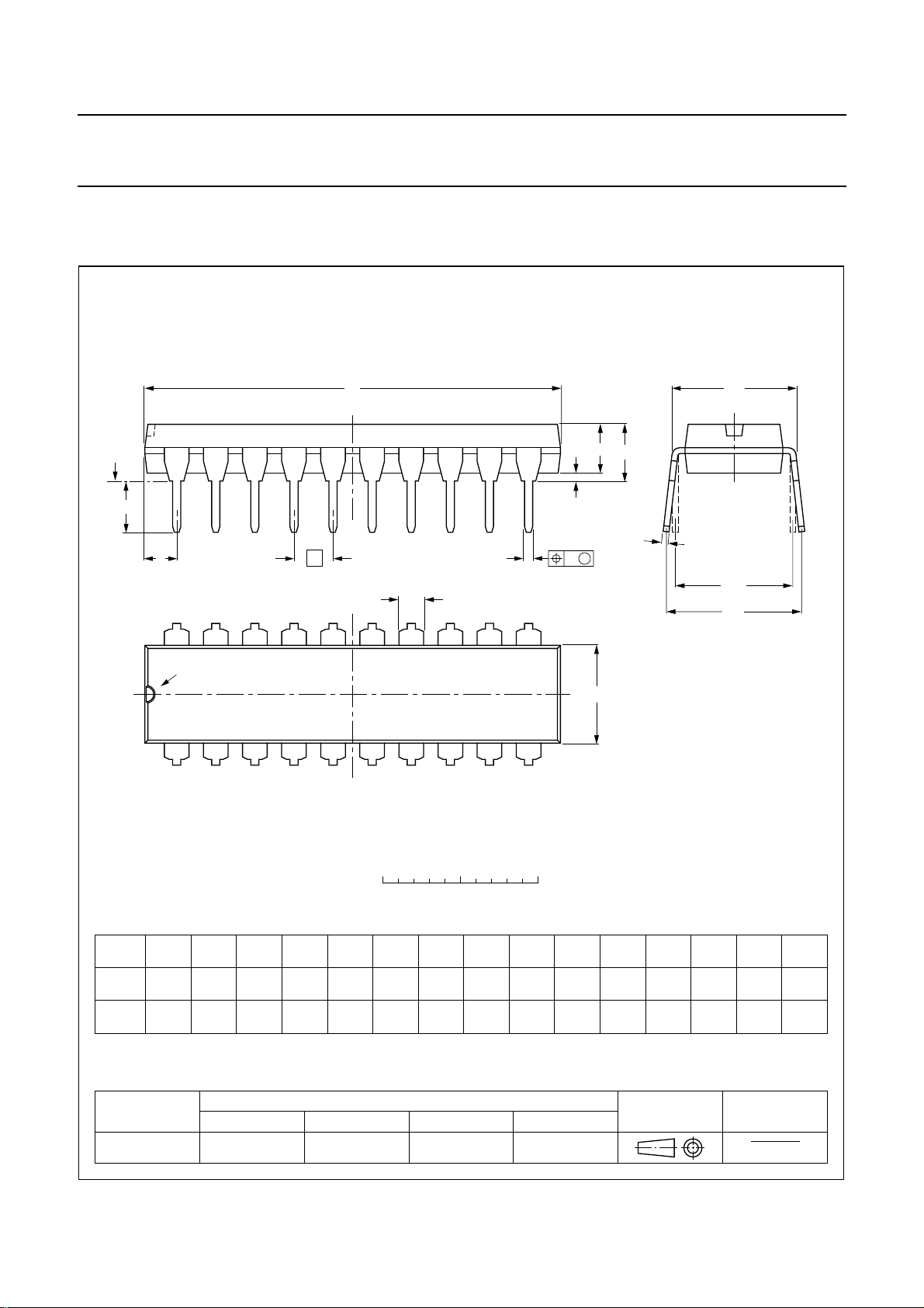
SAA3008P: 20-lead DIL; plastic (SOT146); SOT146-1; 1996 December 6.
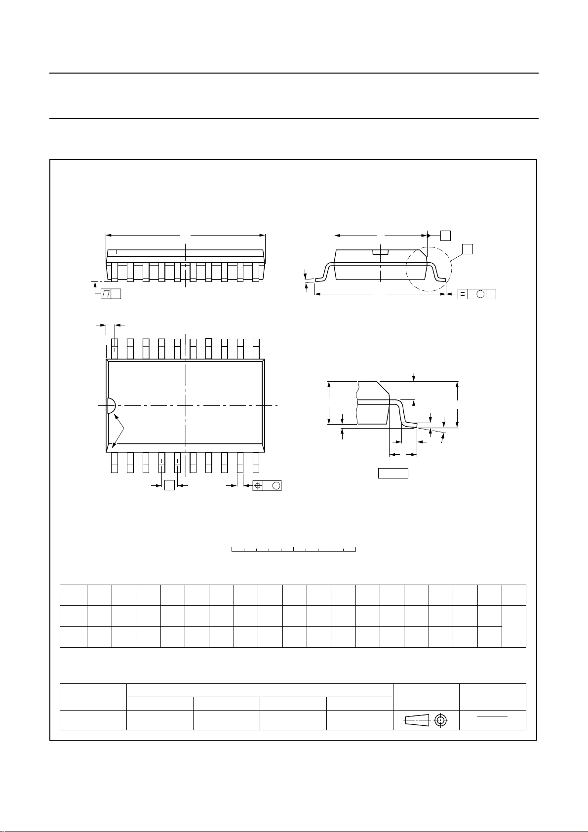
SAA3008T: 20-lead mini-pack; plastic (SO20; SOT163A); SOT163-1; 1996 December 6.
December 1988 2
Page 3

Philips Semiconductors Preliminary specification
Infrared remote control transmitter
(RECS 80 low voltage)
SAA3008
Fig.2 Pinning diagram.
Fig.1 SAA3008 application example.
PINNING
1 REMO remote data output
2 SEN6N
3 SEN5N
4 SEN4N
5 SEN3N
6 SEN2N
7 SEN1N
8 SEN0N
9 ADRM address/mode control input
10 V
11 OSCI oscillator input
12 OSCO oscillator output
13 DRV0N
14 DRV1N
15 DRV2N
16 DRV3N
17 DRV4N
18 DRV5N
19 DRV6N
20 V
SS
DD
sense inputs from key matrix
ground (0 V)
drive outputs to key matrix
positive supply voltage
December 1988 3
Page 4

Philips Semiconductors Preliminary specification
Infrared remote control transmitter
(RECS 80 low voltage)
FUNCTIONAL DESCRIPTION
Key matrix (DRV0N -DRV6N and SEN0N-SEN6N)
The transmitter keyboard is arranged as a scanned matrix
with seven driver outputs (DRV0N to DRV6N) and seven
sensing inputs (SEN0N to SEN6N) as shown in Fig.1.
The driver outputs are open-drain n-channel transistors
which are conductive in the stand-by mode. The sensing
inputs enable the generation of 56 command codes. With
two external diodes connected (or triple contact), as in
Fig.1, all 64 commands are addressable. The sense lines
have p-channel pull-up transistors, so that they are HIGH
until pulled LOW by connecting them to an output via a key
depression to initiate a code transmission.
The maximum allowable value of contact series resistance
for keyboard switches in the ON-state is 7 kΩ.
Address/mode input (ADRM)
Subsystem addresses are defined by connecting one or
two of the key matrix driver lines (DRV0N to DRV6N) to the
ADRM input. This allows up to 20 subsystem addresses to
be generated for the REMO output (bits S3, S2, S1 and
S0) as shown in Table 1 and Fig.3.
The transmission mode is defined by the DRV6N to ADRM
connection as follows:
• Mode 1 DRV6N not connected to ADRM
• Mode 2 DRV6N connected to ADRM
In Mode 1 the reference time REF equals 3To, this may be
used as a reference time for the decoding sequence.
In Mode 2 an additional modulated pulse has been
inserted into the middle of the reference time, therefore,
these pulses are now separated by 1.5To. This unique
start pattern START uses the detection of a beginning
word (see Fig.3).
When more than one connection is made to ADRM then all
connections should be decoupled using diodes.
SAA3008
while the command key is pressed. A chance of the
subsystem address does not start a transmission.
In a multiple keystroke sequence (Fig.6) the second
word B might be transmitted with subsystem address 18 or
19 instead of the preselected subsystem address
(Table 1). This is only relevant for systems decoding
subsystem address 18 or 19.
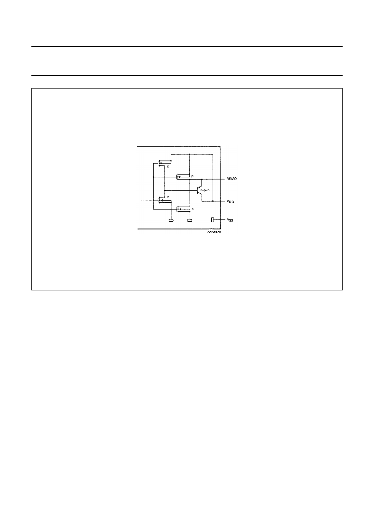
Remote control signal output (REMO) The REMO output driver stage incorporates a bipolar
emitter-follower which allows a high output current in the
output active (HIGH) state (Fig.7).
The information is defined by the distance ‘t
leading edges of the modulated pulses (Fig.4). The
distance tbis a multiple of the basic unit To(Table 3) which
equals 1152 periods of the oscillator frequency f
(Table 3). The pulses are modulated with 6 periods of1⁄
of the oscillator frequency (38 kHz).
The format of the output data is illustrated in Figs 3 and 4.
A data word starts with the reference time and toggle bit T0
and is followed by the definition bits for the subsystem
address S3, S2, S1 and S0 (bit S3 is transmitted only for
subsystem addresses 8 to 20).
The selected command key is defined by bits F, E, D, C, B
and A as shown in Table 2.
The toggle bit T0 acts as an indication for the decoder
whether the next instruction should be considered as a
new command or not. The codes for the subsystem
address and the selected key are given in Table 3.
’ between the
b
osc
12
The ADRM input has switched pull-up and pull-down
loads. In the stand-by mode only pull-down load is active
and ADRM input is held LOW (this condition is
independent of the ADRM circuit configuration and
minimizes power loss in the standby mode). When a key is
pressed the transmitter becomes active pull-down is
switched OFF, pull-up is switched ON) and the driver line
signals are sensed for the subsystem address coding.
The subsystem address is sensed only within the first scan
cycle, whereas the command code is sensed in every
scan. The transmitted subsystem address remains
unchanged if the subsystem address selection is changed
December 1988 4
Page 5

Philips Semiconductors Preliminary specification
Infrared remote control transmitter
(RECS 80 low voltage)
(b) Transmission with start-pattern and subsystem address 8 to 20.
Where:
Reference time
start pattern T0 toggle bit
S3, S2, S1, S0 subsystem address
A to F command bits
t
W word length
binary values determined by pulse spacing
SAA3008
Fig.3 Data format of remote control signal (REMO).
Fig.4 Waveform for one pulse period at REMO output; for timing values see Table 3.
Oscillator (OSCI, OSCO) The external components for the oscillator circuit are connected to OSCI and OSCO. The oscillator operates with a
ceramic resonator in the frequency range 350 kHz to 500 kHz, as defined by the resonator. When operating at a supply
voltage of below 3 V a 270 kHz resistor should be connected in parallel with the resonator.
December 1988 5
Page 6

Philips Semiconductors Preliminary specification
Infrared remote control transmitter
SAA3008
(RECS 80 low voltage)
Table 1 Definition of subsystem addresses
address driver line(s) subsystem address
number connected to ADRM S3 S2 S1 S0
1 no connection − 11 1
2 DRV0N − 00 0
3 DRV1N − 00 1
4 DRV2N − 01 0
5 DRV3N − 01 1
6 DRV4N − 10 0
7 DRV5N − 10 1
8 DRV0N and DRV2N 0 0 0 0
9 DRV0N and DRV3N 1 0 0 0
10 DRV0N and DRV4N 0 1 0 0
11 DRV0N and DRV5N 1 1 0 0
12 DRV1N and DRV2N 0 0 0 1
13 DRV1N and DRV3N 1 0 0 1
14 DRV1N and DRV4N 0 1 0 1
15 DRV1N and DRV5N 1 1 0 1
16 DRV2N and DRV3N 1 0 1 0
17 DRV2N and DRV4N 0 1 1 0
18 DRV2N and DRV5N 1 1 1 0
19 DRV3N and DRV4N 0 1 1 1
20 DRV3N and DRV5N 1 1 1 1
December 1988 6
Page 7

Philips Semiconductors Preliminary specification
Infrared remote control transmitter
SAA3008
(RECS 80 low voltage)
Table 2 Definition of command codes
key drive-to-sense command code generated
pressed connection made F E D C B A
0 DRV0N to SEN0N 0 0 0 0 0 0
1 DRV1N to SEN0N 0 0 0 0 0 1
2 DRV2N to SEN0N 0 0 0 0 1 0
3 DRV3N to SEN0N 0 0 0 0 1 1
4 DRV4N to SEN0N 0 0 0 1 0 0
5 DRV5N to SEN0N 0 0 0 1 0 1
6 DRV6N to SEN0N 0 0 0 1 1 0
7 DRV7N to SEN0N 0 0 0 1 1 1
8 DRV0N to SEN1N 0 0 1 0 0 0
9 DRV1N to SEN1N 0 0 1 0 0 1
10 DRV2N to SEN1N 0 0 1 0 1 0
11 DRV3N to SEN1N 0 0 1 0 1 1
12 DRV4N to SEN1N 0 0 1 1 0 0
13 DRV5N to SEN1N 0 0 1 1 0 1
14 DRV6N to SEN1N 0 0 1 1 1 0
15 DRV7N to SEN1N 0 0 1 1 1 1
16 DRV0N to SEN2N 0 1 0 0 0 0
17 DRV1N to SEN2N 0 1 0 0 0 1
18 DRV2N to SEN2N 0 1 0 0 1 0
19 DRV3N to SEN2N 0 1 0 0 1 1
20 DRV4N to SEN2N 0 1 0 1 0 0
21 DRV5N to SEN2N 0 1 0 1 0 1
22 DRV6N to SEN2N 0 1 0 1 1 0
23 DRV7N to SEN2N 0 1 0 1 1 1
24 DRV0N to SEN3N 0 1 1 0 0 0
25 DRV1N to SEN3N 0 1 1 0 0 1
26 DRV2N to SEN3N 0 1 1 0 1 0
27 DRV3N to SEN3N 0 1 1 0 1 1
28 DRV4N to SEN3N 0 1 1 1 0 0
29 DRV5N to SEN3N 0 1 1 1 0 1
30 DRV6N to SEN3N 0 1 1 1 1 0
31 DRV7N to SEN3N 0 1 1 1 1 1
December 1988 7
Page 8

Philips Semiconductors Preliminary specification
Infrared remote control transmitter
SAA3008
(RECS 80 low voltage)
key drive-to-sense command code generated
pressed connection made F E D C B A
32 DRV0N to SEN4N 1 0 0 0 0 0
33 DRV1N to SEN4N 1 0 0 0 0 1
34 DRV2N to SEN4N 1 0 0 0 1 0
35 DRV3N to SEN4N 1 0 0 0 1 1
36 DRV4N to SEN4N 1 0 0 1 0 0
37 DRV5N to SEN4N 1 0 0 1 0 1
38 DRV6N to SEN4N 1 0 0 1 1 0
39 DRV7N to SEN4N 1 0 0 1 1 1
40 DRV0N to SEN5N 1 0 1 0 0 0
41 DRV1N to SEN5N 1 0 1 0 0 1
42 DRV2N to SEN5N 1 0 1 0 1 0
43 DRV3N to SEN5N 1 0 1 0 1 1
44 DRV4N to SEN5N 1 0 1 1 0 0
45 DRV5N to SEN5N 1 0 1 1 0 1
46 DRV6N to SEN5N 1 0 1 1 1 0
47 DRV7N to SEN5N 1 0 1 1 1 1
48 DRV0N to SEN6N 1 1 0 0 0 0
49 DRV1N to SEN6N 1 1 0 0 0 1
50 DRV2N to SEN6N 1 1 0 0 1 0
51 DRV3N to SEN6N 1 1 0 0 1 1
52 DRV4N to SEN6N 1 1 0 1 0 0
53 DRV5N to SEN6N 1 1 0 1 0 1
54 DRV6N to SEN6N 1 1 0 1 1 0
55 DRV7N to SEN6N 1 1 0 1 1 1
56 DRV0N to SEN5N and SEN6N 1 1 1 0 0 0
57 DRV1N to SEN5N and SEN6N 1 1 1 0 0 1
58 DRV2N to SEN5N and SEN6N 1 1 1 0 1 0
59 DRV3N to SEN5N and SEN6N 1 1 1 0 1 1
60 DRV4N to SEN5N and SEN6N 1 1 1 1 0 0
61 DRV5N to SEN5N and SEN6N 1 1 1 1 0 1
62 DRV6N to SEN5N and SEN6N 1 1 1 1 1 0
63 DRV7N to SEN5N and SEN6N 1 1 1 1 1 1
December 1988 8
Page 9

Philips Semiconductors Preliminary specification
Infrared remote control transmitter
(RECS 80 low voltage)
Table 3 Pulse timing
PARAMETER SYMBOL DURATION DURATION at f
Modulation period
Modulation LOW time
Modulation HIGH time
Modulation pulse width
Basic unit of pulse spacing
Word length for subsystem
addresses
0 to 7
8 to 20
Pulse separation for
logic 0 t
logic 1 t
reference time t
toggle bit t
Start pattern t
t
M 12t
t
ML 8t
t
MH 4t
t
PW
t
o
t
W 55296t
t
W 59904t
b
b
b
b
b
osc
osc
osc
5t
M +tMH 140.8 µs
1152t
2t
o
3t
o
3t
o
2t
o
3t
o
2 × 1.5t
osc
osc
osc
o
OSC
t
= 2.2 µs
OSC
26.4 µs
17.6 µs
8.8 µs
2.53 ms
121.44 ms
132.56 ms
5.06 ms
7.59 ms
7.59 ms
5.06 ms
7.59 ms
2 × 3.79 ms
SAA3008
= 455 kHz;
OPERATION
Keyboard
In the standby mode all drivers DRV0N-DRV6N are ON
but are non-conducting due to their open drain
configuration. When a key is pressed, a completed drain
connection pulls down one or more of the sense lines to
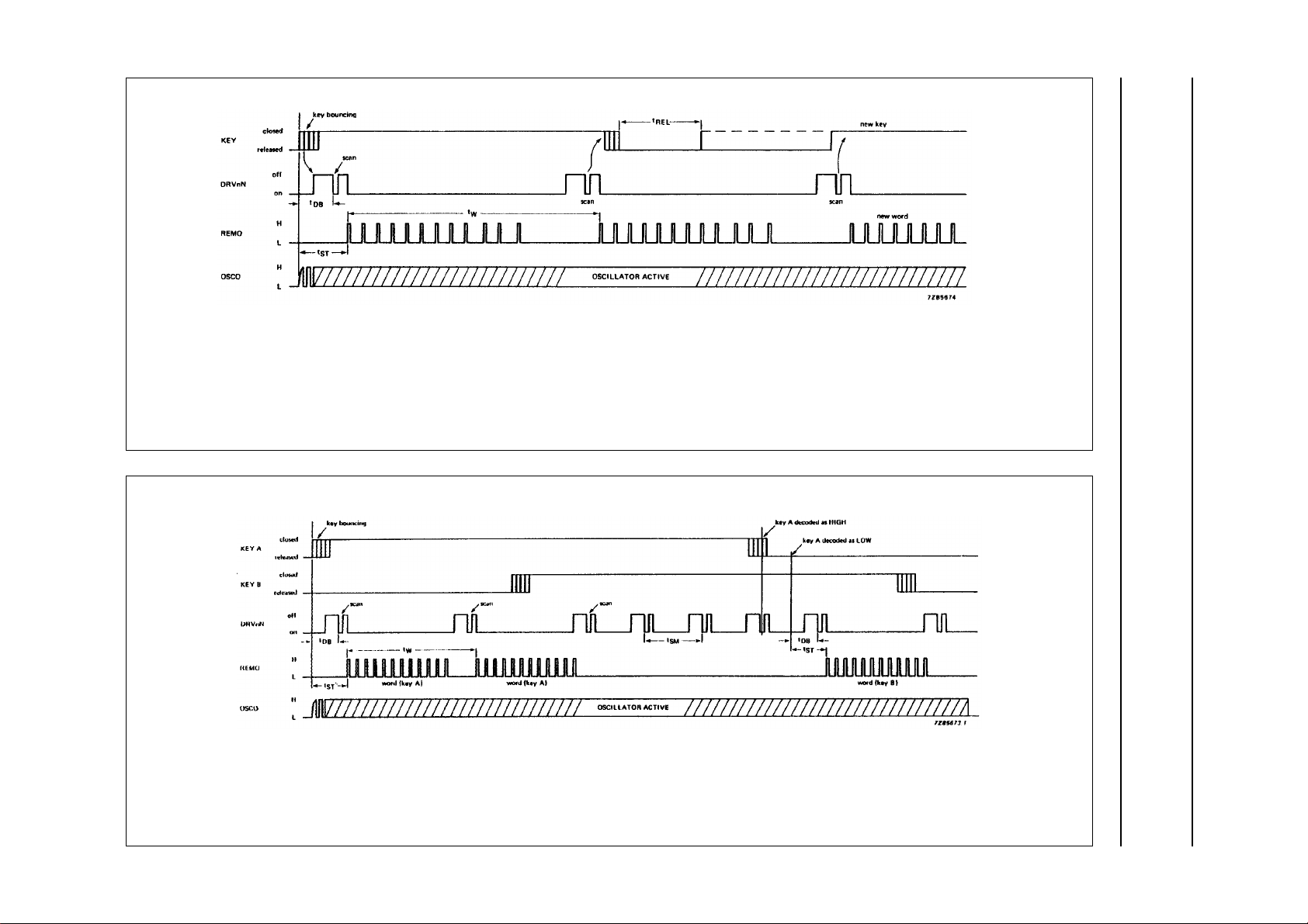
ground. Referring to Fig.5, the power-up sequence for the
IC commences as a key is pressed. The oscillator
becomes active and then, following the debounce time
(t
), the output drivers become active successively.
DB
Within the first scan cycle the transmission mode,
subsystem address and the selected command code are
sensed and loaded into an internal data latch. In a multiple
keystroke sequence (Fig.6) the command code is always
altered according to the sensed key.
Multiple keystroke protection
The keyboard is protected against multiple keystrokes.
If more than one key is pressed the circuit will not generate
a new REMO sequence (Fig.6).
In a multiple keystroke sequence the scan repetition rate
is increased to detect the release of the key as soon as
possible.
There are two restrictions caused by the special structure
of the keyboard matrix:
• The keys switching directly to ground (codes 7, 15, 23,
31, 39, 47, 55, 63) are not completely covered by
multiple keystroke protection. If one sense input is
switched to ground, other keys on that sense line are
ignored.
• The sense lines SEN5N and SEN6N are not protected
against multiple keystrokes on the same driver line
because this has been used to define codes 56 to 63.
Output sequence
The output operation starts when the code of the selected
key has been loaded into the internal command register.
A burst of pulses, including the latched address and
command codes, is generated at the output REMO for as
long as the key is pressed. The format of the output pulse
train is as shown in Figs 3 and 4. The operation is
terminated by releasing the key, or by pressing more than
one key at the same time. Once a sequence has been
started, the transmitted words will always be completed
after the key has been released.
The toggle bit T0 is incremented if the key is released for
a minimum time t
(Fig.5). In a multiple keystroke
REL
sequence the toggle bit remains unchanged.
December 1988 9
Page 10
December 1988 10
Fig.5 Single keystroke sequence;
tDB= debounce time = 4Toto 9To;
tST= start time = 5Toto 10To;
t
= minimum release time = To;
REL
tW= word length.
Philips Semiconductors Preliminary specification
Infrared remote control transmitter
(RECS 80 low voltage)
Fig.6 Scan rate multiple keystroke sequence:
tSM= scan rate (multiple keystroke) = 6Toto 10To;
tDB, tST, and tW are as per Fig.5.
SAA3008
Page 11

Philips Semiconductors Preliminary specification
Infrared remote control transmitter
(RECS 80 low voltage)
RATINGS
Limiting values in accordance with the Absolute Maximum Rating System (IEC 134)
PARAMETER CONDITIONS SYMBOL MIN. MAX. UNIT
Supply voltage range V
Input voltage range V
Output voltage range V
Total power dissipation
DIL package (SOT146) P
mini−pack (SO20; SOT163A) P
Power dissipation
matrix outputs DRV0N to DRV6N P
remote data output REMO P
Operating ambient temperature range T
Storage temperature range T
HANDLING
DD
I
O
tot
tot
O
O
amb
stg
SAA3008
−0.3 +7V
−0.3 VDD+ 0.3 V
−0.3 VDD+ 0.3 V
− 300 mW
− 200 mW
− 50 mW
− 200 mW
−20 +70 °C
−20 +125 °C
Inputs and outputs are protected against electrostatic charge in normal handling. However, to be totally safe, it is
desirable to take normal precautions appropriate to handling MOS devices (see ‘
Handling MOS Devices
’).
CHARACTERISTICS
V
SS
= 0 V; T
= 0 to + 70 °C; unless otherwise specified
amb
PARAMETER CONDITIONS SYMBOL MIN. TYP. MAX. UNIT
Supply voltage V
Supply current active f
Standby mode T
= 455 kHz;
osc
= 3 V I
V
DD
V
= 4.5 V I
DD
V
= 6 V I
DD
= 25 °C;
amb
VDD= 6 V I
DD
DD
DD
DD
DD
2.0 − 6.5 V
− 0.25 − mA
− 0.5 − mA
− 1 − mA
−−4µA
Oscillator frequency
(ceramic resonator) VDD= 2 to 6.5 V f
osc
350 − 500 kHz
Inputs SEN0N to SEN6N
Input voltage LOW VDD= 2 to 6.5 V V
Input voltage HIGH V
= 2 to 6.5 V V
DD
IL
IH
−−0.3 V
0.7 V
DD
−− V
DD
V
Input current
(p-channel pull-up) V
= 0 V
IL
V
= 2 V I
DD
= 6.5 V I
V
DD
I
I
−10 −−100 µA
−100 −−600 µA
December 1988 11
Page 12

Philips Semiconductors Preliminary specification
Infrared remote control transmitter
(RECS 80 low voltage)
PARAMETER CONDITIONS SYMBOL MIN. TYP. MAX. UNIT
Outputs DRV0N to DRV6N
(open drain 1)
Output voltage ON IO= 0.25 mA
V
= 2 V V
DD
I
= 2.5 mA
O
= 6.5 V V
V
DD
Output current OFF V
Input ADRM
Input voltage LOW V
Input voltage HIGH V
Input current
(switched p and n
channel pull-up and
pull-down)
pull-up active V
pull-down active V
Output REMO
Output voltage HIGH IOH= −40 mA;
Output voltage LOW I
Input OSCI
Input current HIGH V
Output OSCO
Output voltage HIGH I
Output voltage LOW I
= 6.5 V I
DD
= 0 V
I
V
= 2 V I
DD
V
= 6.5 V I
DD
I=VDD
VDD= 2 V I
V
= 6.5 V I
DD
T
= 25 °C
amb
V
= 2 V V
DD
V
= 6.5 V V
DD
I
= 0.5 mA;
OH
= 2 V V
V
DD
= 0.5 mA;
OL
V
= 2 V V
DD
I
= 2.0 mA;
OL
V
= 6.5 V V
DD
= 6.5 V I
DD
= 100 µA;
OH
VDD= 6.5 V
= 100 µA;
OL
VDD= 6.5 V
SAA3008
OL
OL
O
IL
IH
IL
IL
IH
IH
OH
OH
OH
OL
OL
IH
V
OH
V
OL
−−0.3 V
−−0.6 V
−−10 µA
−−0.4 V
0.85 V
DD
−− V
DD
V
−10 −−100 µA
−100 −−600 µA
10 − 100 µA
100 − 600 µA
0.8 −− V
5.0 −− V
0.8 V
DD
−− V
−−0.4 V
−−0.4 V
3.0 − 7.0 µA
VDD−0.8 −− V
−−0.7 V
December 1988 12
Page 13
Philips Semiconductors Preliminary specification
Infrared remote control transmitter
(RECS 80 low voltage)
SAA3008
Fig.7 REMO output stage.
December 1988 13
Page 14
Philips Semiconductors Preliminary specification
Infrared remote control transmitter
(RECS 80 low voltage)
PACKAGE OUTLINES
DIP20: plastic dual in-line package; 20 leads (300 mil)
D
seating plane
L
Z
20
e
b
SAA3008
SOT146-1
M
E
A
2
A
A
1
w M
b
1
11
c
(e )
1
M
H
pin 1 index
1
0 5 10 mm
scale
DIMENSIONS (inch dimensions are derived from the original mm dimensions)
A
A
A
UNIT
inches
Note
1. Plastic or metal protrusions of 0.25 mm maximum per side are not included.
max.
mm
OUTLINE
VERSION
SOT146-1
1 2
min.
max.
1.73
1.30
0.068
0.051
IEC JEDEC EIAJ
b
b
1
0.53
0.38
0.021
0.015
0.36
0.23
0.014
0.009
REFERENCES
cD E e M
(1) (1)
26.92
26.54
1.060
1.045
SC603
6.40
6.22
0.25
0.24
E
10
(1)
M
e
L
1
3.60
8.25
3.05
7.80
0.14
0.32
0.12
0.31
EUROPEAN
PROJECTION
H
E
10.0
0.2542.54 7.62
8.3
0.39
0.010.10 0.30
0.33
ISSUE DATE
w
92-11-17
95-05-24
Z
max.
2.04.2 0.51 3.2
0.0780.17 0.020 0.13
December 1988 14
Page 15
Philips Semiconductors Preliminary specification
Infrared remote control transmitter
(RECS 80 low voltage)
SO20: plastic small outline package; 20 leads; body width 7.5 mm
D
c
y
Z
20
11
SAA3008
SOT163-1
E
H
E
A
X
v M
A
pin 1 index
1
e
0 5 10 mm
DIMENSIONS (inch dimensions are derived from the original mm dimensions)
mm
A
max.
2.65
0.10
A
1
0.30
0.10
0.012
0.004
A2A
2.45
2.25
0.096
0.089
0.25
0.01
b
0.49
0.36
p
cD
0.32
0.23
0.013
0.009
3
0.019
0.014
UNIT
inches
Note
1. Plastic or metal protrusions of 0.15 mm maximum per side are not included.
10
w M
b
p
scale
(1)E(1) (1)
13.0
12.6
0.51
0.49
eHELLpQ
7.6
1.27
7.4
0.30
0.050
0.29
10.65
10.00
0.419
0.394
Q
A
2
A
1
1.4
0.055
1.1
0.4
0.043
0.016
detail X
1.1
1.0
0.043
0.039
(A )
L
p
L
0.25
0.01
A
3
θ
0.25 0.1
0.01
ywv θ
Z
0.9
0.4
8
0.004
0.035
0.016
0
o
o
OUTLINE
VERSION
SOT163-1
IEC JEDEC EIAJ
075E04 MS-013AC
REFERENCES
December 1988 15
EUROPEAN
PROJECTION
ISSUE DATE
95-01-24
97-05-22
Page 16

Philips Semiconductors Preliminary specification
Infrared remote control transmitter
(RECS 80 low voltage)
SOLDERING
Introduction
There is no soldering method that is ideal for all IC
packages. Wave soldering is often preferred when
through-hole and surface mounted components are mixed
on one printed-circuit board. However, wave soldering is
not always suitable for surface mounted ICs, or for
printed-circuits with high population densities. In these
situations reflow soldering is often used.
This text gives a very brief insight to a complex technology.
A more in-depth account of soldering ICs can be found in
our
“IC Package Databook”
DIP
SOLDERING BY DIPPING OR BY WAVE
The maximum permissible temperature of the solder is
260 °C; solder at this temperature must not be in contact
with the joint for more than 5 seconds. The total contact
time of successive solder waves must not exceed
5 seconds.
The device may be mounted up to the seating plane, but
the temperature of the plastic body must not exceed the
specified maximum storage temperature (T
printed-circuit board has been pre-heated, forced cooling
may be necessary immediately after soldering to keep the
temperature within the permissible limit.
R
EPAIRING SOLDERED JOINTS
Apply a low voltage soldering iron (less than 24 V) to the
lead(s) of the package, below the seating plane or not
more than 2 mm above it. If the temperature of the
soldering iron bit is less than 300 °C it may remain in
contact for up to 10 seconds. If the bit temperature is
between 300 and 400 °C, contact may be up to 5 seconds.
SO
REFLOW SOLDERING
Reflow soldering techniques are suitable for all SO
packages.
(order code 9398 652 90011).
). If the
stg max
SAA3008
Several techniques exist for reflowing; for example,
thermal conduction by heated belt. Dwell times vary
between 50 and 300 seconds depending on heating
method. Typical reflow temperatures range from
215 to 250 °C.
Preheating is necessary to dry the paste and evaporate
the binding agent. Preheating duration: 45 minutes at
45 °C.
AVE SOLDERING
W
Wave soldering techniques can be used for all SO
packages if the following conditions are observed:
• A doublewave (a turbulent wave with high upward
pressure followed by a smooth laminar wave) soldering
technique should be used.
• The longitudinal axis of the package footprint must be
parallel to the solder flow.
• The package footprint must incorporate solder thieves at
the downstream end.
During placement and before soldering, the package must
be fixed with a droplet of adhesive. The adhesive can be
applied by screen printing, pin transfer or syringe
dispensing. The package can be soldered after the
adhesive is cured.
Maximum permissible solder temperature is 260 °C, and
maximum duration of package immersion in solder is
10 seconds, if cooled to less than 150 °C within
6 seconds. Typical dwell time is 4 seconds at 250 °C.
A mildly-activated flux will eliminate the need for removal
of corrosive residues in most applications.
R
EPAIRING SOLDERED JOINTS
Fix the component by first soldering two diagonallyopposite end leads. Use only a low voltage soldering iron
(less than 24 V) applied to the flat part of the lead. Contact
time must be limited to 10 seconds at up to 300 °C. When
using a dedicated tool, all other leads can be soldered in
one operation within 2 to 5 seconds between
270 and 320 °C.
Reflow soldering requires solder paste (a suspension of
fine solder particles, flux and binding agent) to be applied
to the printed-circuit board by screen printing, stencilling or
pressure-syringe dispensing before package placement.
December 1988 16
Page 17

Philips Semiconductors Preliminary specification
Infrared remote control transmitter
SAA3008
(RECS 80 low voltage)
DEFINITIONS
Data sheet status
Objective specification This data sheet contains target or goal specifications for product development.
Preliminary specification This data sheet contains preliminary data; supplementary data may be published later.
Product specification This data sheet contains final product specifications.
Limiting values
Limiting values given are in accordance with the Absolute Maximum Rating System (IEC 134). Stress above one or
more of the limiting values may cause permanent damage to the device. These are stress ratings only and operation
of the device at these or at any other conditions above those given in the Characteristics sections of the specification
is not implied. Exposure to limiting values for extended periods may affect device reliability.
Application information
Where application information is given, it is advisory and does not form part of the specification.
LIFE SUPPORT APPLICATIONS
These products are not designed for use in life support appliances, devices, or systems where malfunction of these
products can reasonably be expected to result in personal injury. Philips customers using or selling these products for
use in such applications do so at their own risk and agree to fully indemnify Philips for any damages resulting from such
improper use or sale.
December 1988 17
 Loading...