

Page 1
INTEGRATED CIRCUITS
DATA SH EET
SAA1101
Universal sync generator (USG)
Product specification
File under Integrated Circuits, IC02
January 1990
Page 2
Philips Semiconductors Product specification
Universal sync generator (USG) SAA1101
FEATURES
• Programmable to seven standards
• Additional outputs to simplify signal processing
• Can be synchronized to an external sync. signal
• Option to select the 524/624 line mode instead of the 525/625 line mode
• Lock from subcarrier to line frequency
GENERAL DESCRIPTION
The SAA1101 is a Universal Sync Generator (USG) and is designed for application in video sources such as cameras,
film scanners, video generators and associated apparatus. The circuit can be considered as a successor to the SAA1043
sync generator and the SAA1044 subcarrier coupling IC.
QUICK REFERENCE DATA
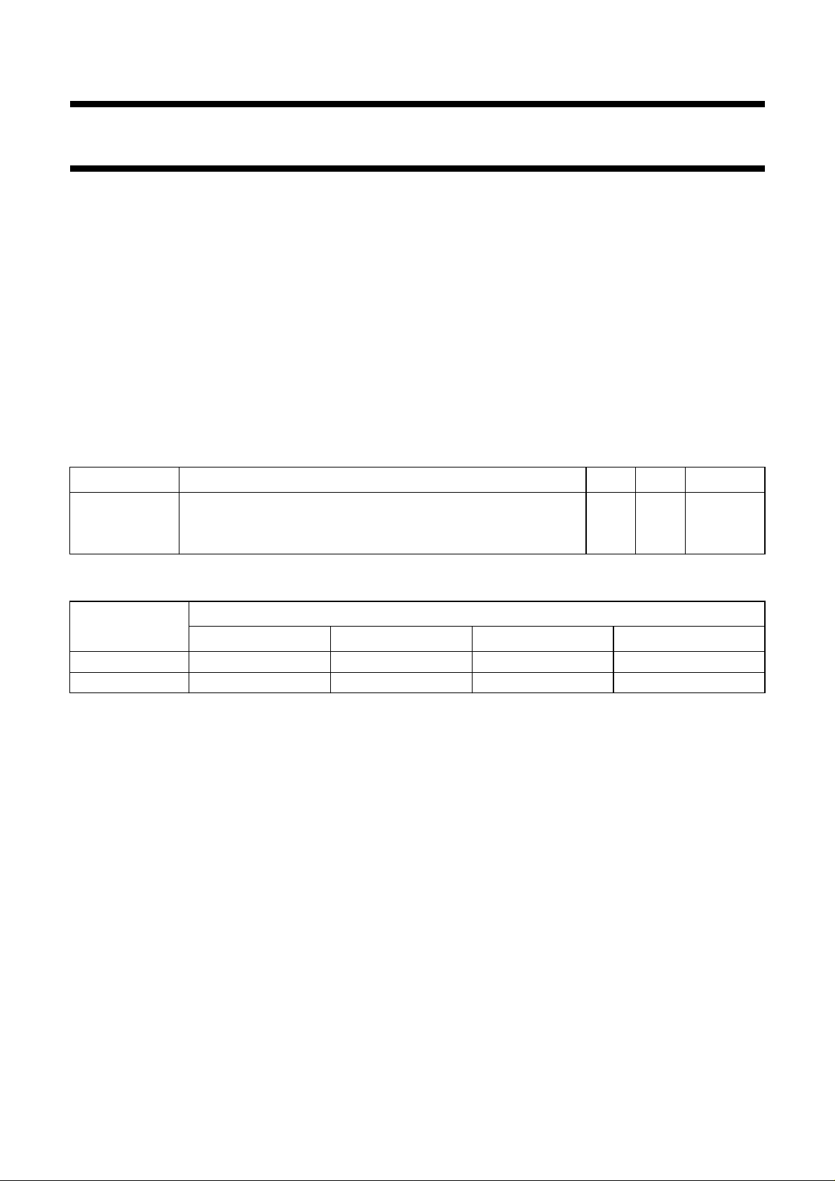
SYMBOL PARAMETER MIN. MAX. UNIT
V
I
DD
f
OSC
DD
supply voltage range (pin 28) 4.5 5.5 V
quiescent supply current − 10 µA
clock oscillator frequency − 24 MHz
ORDERING AND PACKAGE INFORMATION
EXTENDED
TYPE NUMBER
PINS PIN POSITION MATERIAL CODE
PACKAGE
SAA1101P 28 DIL plastic SOT117
SAA1101T 28 SO28 plastic SOT136A
Notes
1. SOT117-1; 1996 December 02.
2. SOT136-1; 1996 December 02.
(1)
(2)
January 1990 2
Page 3
Philips Semiconductors Product specification
Universal sync generator (USG) SAA1101
, full pagewidth
CSCBBKIDHDVDWMP
18171615222120
13232434
LOGIC
COMBINING
CLP12RR
19
VLE11ECS
7
MGH191
SAA1101
PULSE
DIVIDER
VERTICAL
NORM SI
LOGIC
ADDITION/
SUPPRESSION
H
2f
LINE
DIVIDER
RESET
H
40f
SHAPER
VERTICAL
DETECTION
LOCK
VERTICAL
DETECTION
HORIZONTAL
H
f
HRI
ref
H
H
f
DIVIDER
SUBCARRIER
− ∆f
s
f
PHASE
SELECTION
LOCK MODE
DETECTION
81428 910
PH LM1 LM0
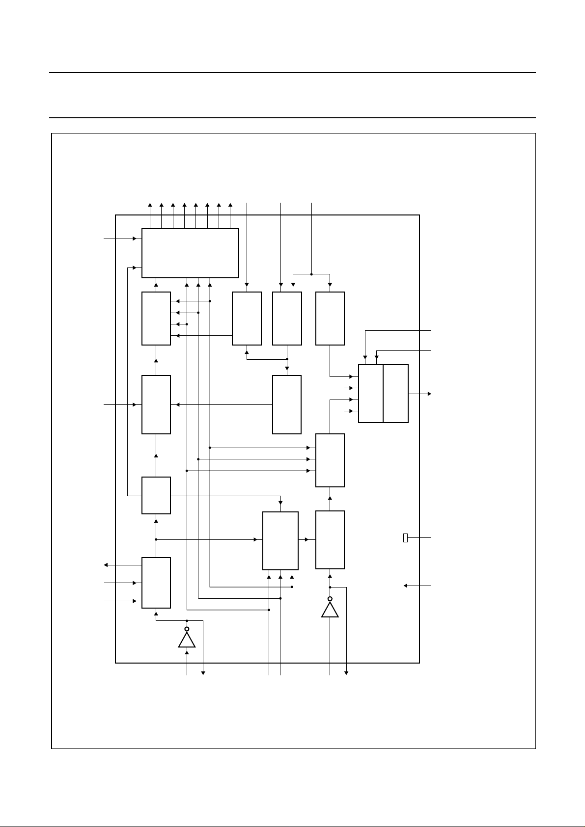
Fig.1 Block diagram.
H
CS1 CLOCS0
160f
PRESCALER
5
OSCI
6
OSCO
STANDARD
PROGRAMMED
252627
X
Y
January 1990 3
∆f
DIVIDER
Z
SUBCARRIER
SUBTRACTION
s
f
2
1
FSI
FSO
SS
V
DD
V
Page 4
Philips Semiconductors Product specification
Universal sync generator (USG) SAA1101
PINNING
SYMBOL PIN DESCRIPTION
page
FSI
FSO
CS1
CS0
OSCI
OSCO
VLE
PH
LM1
LM0
ECS
RR
V
SS
1
2
3
4
5
6
7
SAA1101
8
9
10
11
12
SI
13
MGH190
28
27
26
25
24
23
22
21
20
19
18
17
16
1514
V
DD
Z
Y
X
CLO
NORM
HD
VD
WMP
CLP
CS
CB
BK
ID
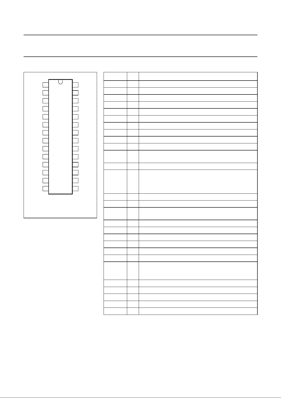
Fig.2 Pinning configuration;
SOT117.
FUNCTIONAL DESCRIPTION
Generation of pulses
Generation of standard pulses such
as sync, blanking and burst for TV
systems: PAL B/G, PALN, PALM,
SECAM and NTSC. In addition a
number of non-standard pulses have
been supplied to simplify signal
processing. These signals include horizontal drive, vertical drive, clamp
pulse, identification etc. It is possible
to select the 524/624 line mode
instead of the 525/625 line mode for
all the above TV systems for
applications such as robotics, games
and computers.
FSI 1 subcarrier oscillator input, where f
FSO 2 subcarrier oscillator output
CS1 3 clock frequency selection - CMOS input
CS0 4 clock frequency selection - CMOS input
OSCI 5 clock oscillator input, where f
max
OSCO 6 clock oscillator output
VLE 7 vertical in-lock enable - CMOS input
PH 8 phase detector output - 3-state output
LM1 9 lock mode selection - CMOS input
LM0 10 lock mode selection - CMOS input
ECS 11 external composite sync. signal - CMOS Schmitt-trigger
input
RR 12 frame reset - CMOS Schmitt-trigger input
SI 13 set identification, used to set the correct field sequence in
P AL-mode. The correction (inversion of fH2) is done at the
left-hand slope of the SI-pulse. Minimum pulse width is
800 ns. CMOS Schmitt-trigger input.
V
SS
14 ground
ID 15 identification - push-pull output
BK 16 burst key (PAL/NTSC), chroma-blanking (SECAM) -
push-pull output
CB 17 composite blanking - push-pull output
CS 18 composite sync. - push-pull output
CLP 19 clamp pulse - push-pull output
WMP 20 white measurement pulse-3-state output
VD 21 vertical drive pulse - push-pull output
HD 22 horizontal drive pulse - push-pull output
NORM 23 used with X, Y and Z to select TV system; NORM = 0,
625/525 line mode (standard);
NORM = 1, 624/524 line mode - CMOS input
CLO 24 clock output - push-pull output
X 25 TV system selection input - CMOS input
Y 26 TV system selection input - CMOS input
Z 27 TV system selection input - CMOS input
V
DD
28 voltage supply
= 5 MHz
max
= 24 MHz
January 1990 4
Page 5
Philips Semiconductors Product specification
Universal sync generator (USG) SAA1101
Lock modes
The USG offers four lock modes:
• Lock from the subcarrier
• Slow sync. lock, external H
• Slow sync. lock, internal H
• Fast sync. lock, internal H
ref
ref
ref
LOCK FROM SUBCARRIER
Lock from subcarrier to the line frequency for the above
mentioned TV systems is given below; the horizontal
frequency (fH) = 15.625 kHz for 625 line systems and
15.734264 kHz for 525 line systems.
SECAM (1 and 2) 282f
PALN 229.2516f
NTSC (1 and 2) 227.5f
PALM 227.25f
PAL B/G 283.7516f
H
H
H
H
H
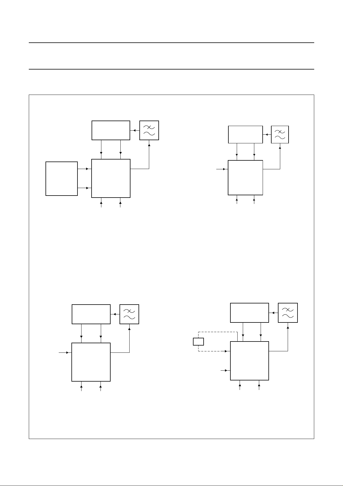
These relationships are obtained by the use of a phase
locked loop and the internal programmed divider chain,
see Fig.3(a).
subcarrier input is, in this case, used as an external
input for the horizontal reference, see Fig.3(d).
SELECTION OF LOCK MODE
Lock mode is selected using the inputs LM0 and LM1 as
illustrated in the Table below.
LM0 LM1 SELECTION
0 0 lock to subcarrier
0 1 slow sync. lock external H
1 0 slow sync. lock internal H
1 1 fast sync. lock internal H
ref
ref
ref
LOCK TO AN EXTERNAL SIGNAL SOURCE
The following methods can be used to lock to an external
signal source:
1. Sync. lock slow; the line frequency is locked to an
external signal. The line and frame information are
extracted from the external sync. signal and used
separately in the lock system. The line information is
used in a phase-locked loop where external and
internal line frequencies are compared by the same
phase detector as is used for the subcarrier lock. The
external frame information is compared with the
internal frame in a slow lock system; mismatch of
internal and external frames will result in the addition
or suppression of one line depending on the direction
of the fault. The maximum lock time for frame lock is
6.25 s, see Fig.3(b).
2. Sync. lock fast. A fast lock of frames is possible with a
frame reset which is extracted out of the incoming
external sync. signal, see Fig.3(c).
3. Sync. lock with external reference. Lock of an external
sync. signal to the line frequency with an external line
reference to make possible a shifted lock. The
January 1990 5
Page 6
Philips Semiconductors Product specification
Universal sync generator (USG) SAA1101
The different lock modes are illustrated by the following figures:
handbook, halfpage
SUB-
CARRIER
OSCILLATOR
Fig.3 (a) Lock to subcarrier.
n × f
H
LINE
OSCILLATOR
OSCO OSCI
FSI
FSO
65
1
SAA1101
2
10
logic 0 logic 1
PH
8
9
LM1LM0
MGH193
handbook, halfpage
ECS
n × f
H
LINE
OSCILLATOR
OSCO OSCI
65
11
SAA1101
10
logic 1 logic 1
9
Fig.3 (c) Fast sync lock, internal H
PH
8
LM1LM0
MGH195
ref
handbook, halfpage
OSCO OSCI
ECS
Fig.3 (b) Slow sync lock, internal H
n × f
H
LINE
OSCILLATOR
65
11
SAA1101
10
logic 0 logic 1
9
PH
8
LM1LM0
MGH194
ref
January 1990 6
handbook, halfpage
τ
H
ref
n × f
H
LINE
OSCILLATOR
H
D OSCO OSCI
65
22
FSI
1
ECS
SAA1101
11
10
logic 0 logic 1
9
LM1LM0
PH
8
MGH192
Fig.3 (d) Slow sync lock, external H
ref
Page 7
Philips Semiconductors Product specification
Universal sync generator (USG) SAA1101
LOCK WITH HORIZONTAL AND VERTICAL SIGNALS
(slow lock modes only)
It is possible to use horizontal and vertical signals instead of composite sync signals. The connections in this situation
are: the external horizontal signal is connected to the ECS input (pin 11) and the vertical signal to the RR input (pin 12).
The HIGH time of the horizontal pulse must be less than 14.4 µs, otherwise it will be detected as being a vertical pulse
and will corrupt the vertical slow lock system.
Selection of Clock Frequency
The clock frequency is selected using the CS0 and CS1 inputs as illustrated below.
CS0 CS1 FREQUENCY 625 LINES 525 LINES UNITS
0 0 160f
0 1 160f
1 0 960f
1 1 1440f
H
H
H
H
2.5 2.517482 MHz
5 5.034964 MHz
15 15.104893 MHz
22.5 22.657340 MHz
Where the horizontal frequency, f
= 15.625 kHz for 625 lines and 15.734264 kHz for 525 lines.
H
Oscillators
The subcarrier oscillator has FSI as its input and FSO as its output. It is always used as a crystal oscillator with a series
resonance crystal with parallel load capacitor. The maximum frequency, f
= 5 MHz and the load capacitor,
max
CL=10<CL<35 pF.
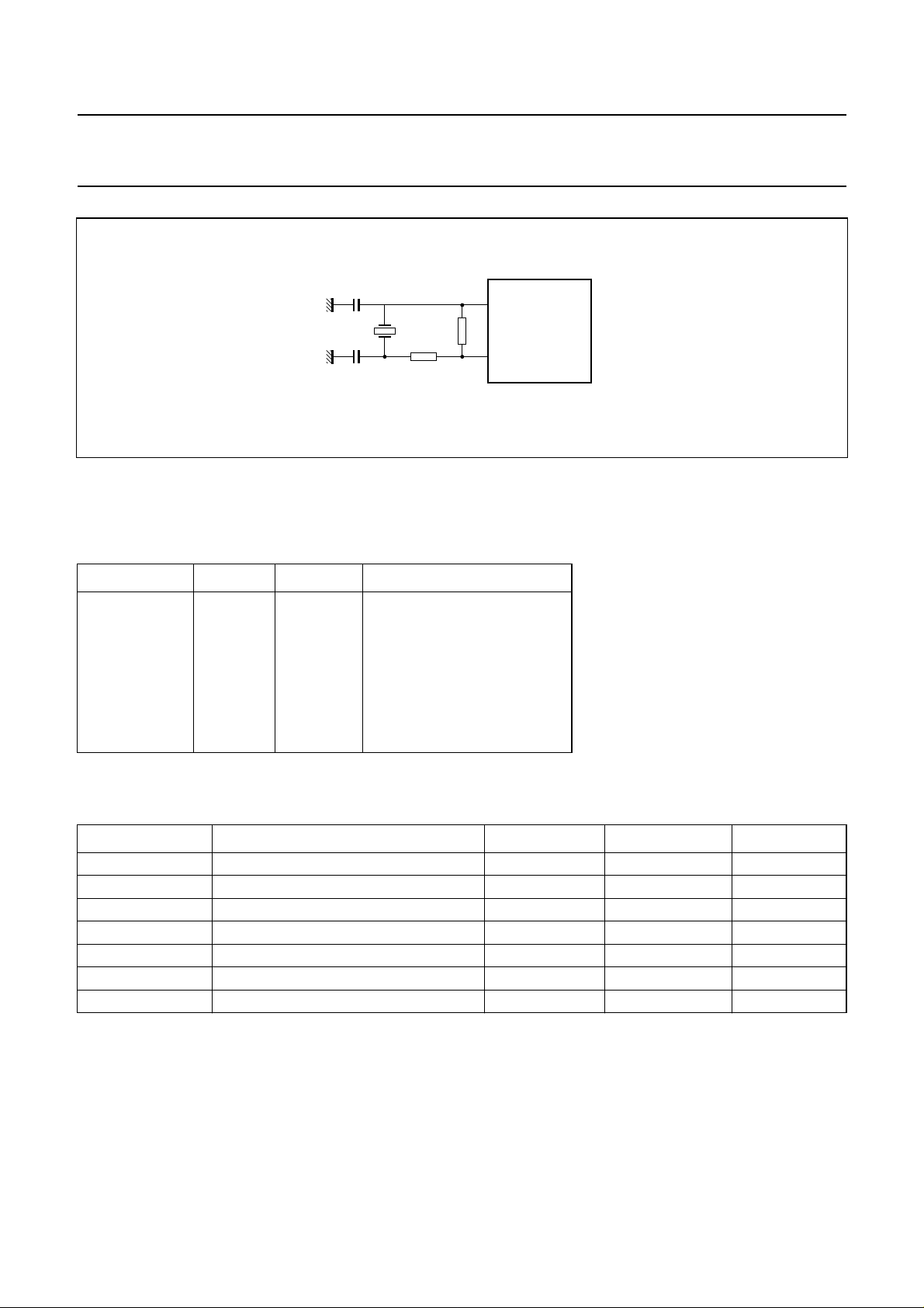
The clock oscillator has OSCI as its input and OSCO as its output. It can be used with an LC oscillator or a series
resonance crystal with parallel load capacitor (Fig.4). The maximum frequency, f
= 24 MHz and the load capacitor,
max
CL = 10 < CL< 35 pF.
Selection of 625/525 (standard; interlaced mode) or 624/524 lines (non-interlaced mode)
Selection is achieved using the NORM input. When NORM = 0, 625/525 (standard) lines are selected;
when NORM = 1, 624/524 line are selected.
Output Dimensions
All push-pull outputs: standard output 2 mA.
White measurement pulse, WMP: 3-state output 2 mA.
Phase detector, PH: 3-state output 2 mA.
January 1990 7
Page 8
Philips Semiconductors Product specification
Universal sync generator (USG) SAA1101
handbook, halfpage
39 pF
15 MHz
39 pF
500 kΩ
1 kΩ
OSCI
OSCO
5
SAA1101
6
MGH196
Fig.4 Crystal oscillator circuit.
Selection of TV System
Selection of the required TV system is achieved by the X, Y and Z inputs as illustrated by the following Table.
SYSTEM
XY Z
SECAM1 0 0 0
PALN 0 0 1
NTSC1 0 1 0
PALM 0 1 1
SECAM2 1 0 0 (with identifier)
PAL B/G 1 0 1
NTSC2 1 1 0 (short blanking)
LIMITING VALUES
Limiting values in accordance with the Absolute Maximum System (IEC 134)
SYMBOL PARAMETER MIN. MAX. UNIT
V
DD
V
I
I
I
I
O
I
DD
P
tot
T
stg
supply voltage −0.5 +7V
input voltage −0.5 VDD+ 0.5
(1)
maximum input current −±10 mA
maximum output current −±10 mA
maximum supply current in V
DD
− 25 mA
maximum power dissipation − 400 mW
storage temperature range −55 +150 °C
Note
1. Input voltage should not exceed 7 V.
January 1990 8
V
Page 9
Philips Semiconductors Product specification
Universal sync generator (USG) SAA1101
CHARACTERISTICS
V
= 4.5 to 5.5 V; T
DD
SYMBOL PARAMETER CONDITIONS MIN. TYP. MAX. UNIT
Supplies
V
DD
I
DD
Inputs
±I
I
CMOS COMPATIBLE; X, Y, Z, NORM, CS0, CS1, LM0, LM1 AND VLE
V
IH
V
IL
SCHMITT TRIGGER INPUTS; ECS, RR AND SI
V
T+
V
T−
V
H
OSCILLATOR INPUTS; OSCI AND FSI
V
IH
V
IL
Outputs
PUSH-PULL OUTPUTS; CB, CS, BK, ID, HD, VD, CLP AND CLO
V
OH
V
OL
OSCILLATOR OUTPUTS; OSCO AND FSO
V
OH
V
OL
3-STATE OUTPUTS; WMP AND PH
V
OH
V
OL
±I
OZ
= −25 to +70 °C unless otherwise specified
amb
supply voltage 4.5 − 5.5 V
supply current (quiescent) T
input leakage current T
= 25 °C −−10 µA
amb
= 25 °C −−100 nA
amb
input voltage HIGH 0.7VDD−− V
input voltage LOW −−0.3V
DD
V
positive-going threshold − 2.5 4 V
negative-going threshold 1 1.5 − V
hysteresis 0.4 1 − V
input voltage HIGH 0.7VDD−− V
input voltage LOW −−0.3V
DD
V
output voltage HIGH −IO = 2 mA; VDD = 5 V 4.5 −− V
output voltage LOW IO = 2 mA; VDD = 5 V −−0.5 V
output voltage HIGH −IO= 0.75 mA; VDD= 5 V 4.5 −− V
output voltage LOW IO = 0.75 mA; VDD=5 V −−0.5 V
output voltage HIGH −IO = 2 mA; VDD = 5V 4.5 −− V
output voltage LOW IO = 2 mA; VDD = 5V −−0.5 V
OFF-state current T
= 25 °C −−50 nA
amb
January 1990 9
Page 10
Philips Semiconductors Product specification
Universal sync generator (USG) SAA1101
OUTPUT WAVEFORMS
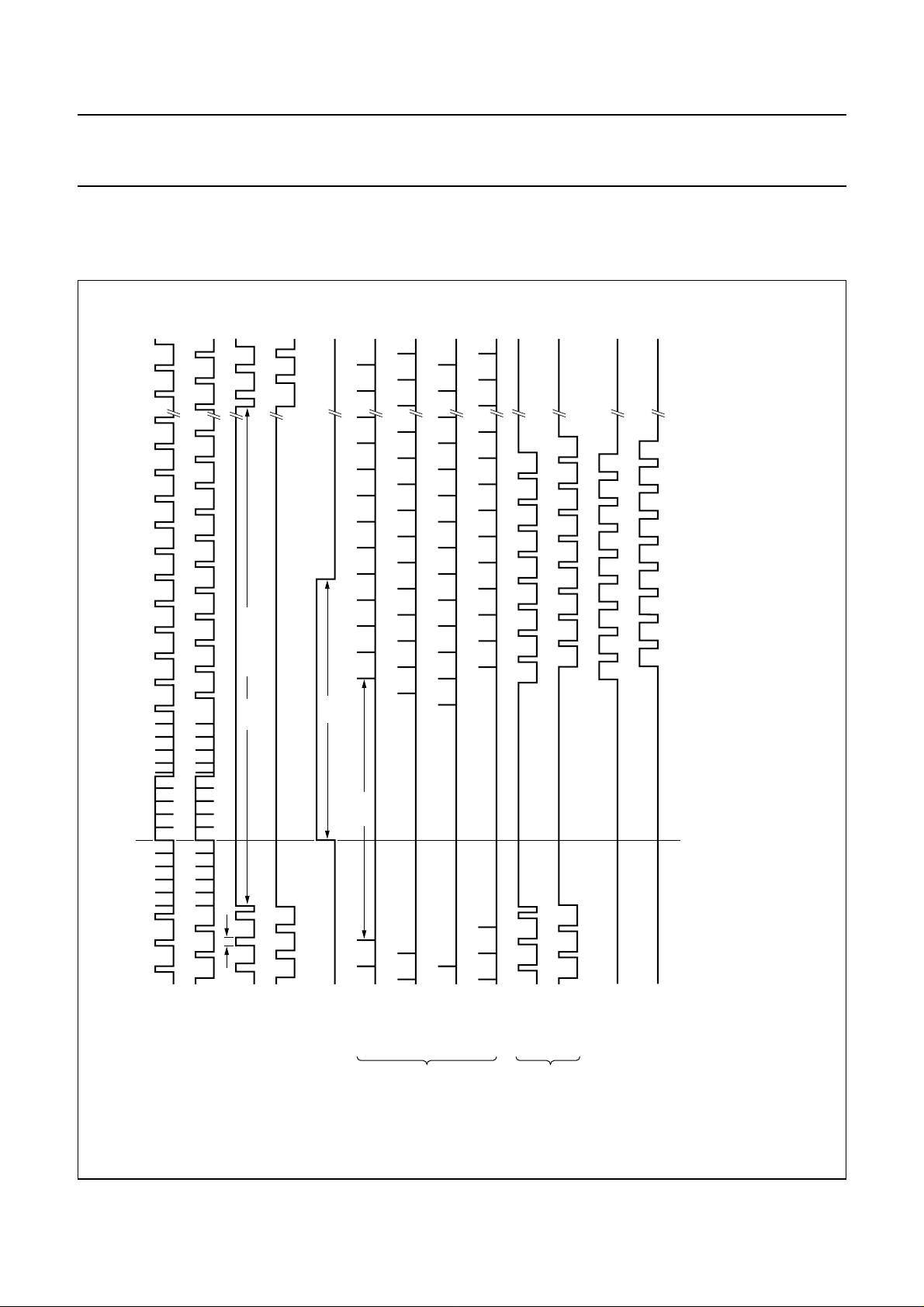
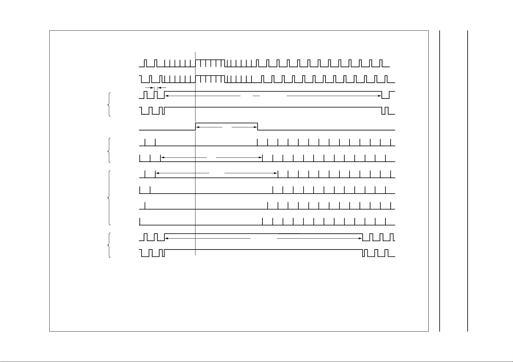
The output waveforms for the different modes of operation are illustrated by Figs 5 and 6.
MGH198
ull pagewidth
start half picture
picture
1st half
2nd half
CS
CS
WCB
t
picture
WCB
25H + t
picture
1st half
CB
picture
2nd half
CB
10H
VD
(1)
9H
picture
1st half
BK
picture
2nd half
BK
picture
3rd half
BK
picture
4th half
BK
picture
1st half
BK
picture
2nd half
BK
picture
1st half
ID
picture
2nd half
ID
CCIR/PAL
January 1990 10
SECAM−1
picture of PAL/CCIR and are not interlaced.
(1) H = 1 horizontal scan.
Fig.5 Typical output waveforms for PAL/CCIR and SECAM. In the 624-line mode the output waveforms are identical to the first half
Page 11
January 1990 11
u
NTSC 1
(2)
CS
CS
CB
CB
1st half
picture
2nd half
picture
1st half
picture
2nd half
picture
t
WCB
start half picture
ll pagewidth
21H + t
Philips Semiconductors Product specification
Universal sync generator (USG) SAA1101
WCB
VD
1st half
BK
BK
BK
BK
BK
BK
CB
CB
picture
2nd half
picture
1st half
picture
2nd half
picture
3rd half
picture
4th half
picture
1st half
picture
2nd half
picture
NTSC 1 + 2
(2)
PAL−M
NTSC 2
(2)
(1) H = 1 horizontal scan.
(2) NTSC mode reset; the fourth half picture is identical to the second half picture for NTSC.
9H
11H
6H
(1)
19H + t
WCB
MGH197
Fig.6 Typical output waveforms for NTSC and PAL-M. In the 524-line mode the output waveforms are identical to the first half picture of NTSC
and are not interlaced.
Page 12
Philips Semiconductors Product specification
Universal sync generator (USG) SAA1101
WAVEFORM TIMING
The waveform timing depends on the frequency of the oscillator input (f
number (N) of oscillations at OSCI. The timings are derived from N × t
One horizontal scan (H) = 320 × t
Where t
= 200 ns for PAL/SECAM and 198.6 ns for NTSC/PAL-M
OSCI
OSCI
=1/fH.
SYMBOL PARAMETER PAL NTSC PAL-M SECAM UNIT N
Composite sync (CS)
t
WSC1
horizontal sync pulse
4.8 4.77 4.77 4.8 µs24
width
t
WSC2
t
WSC3
− duration of
equalizing pulse width 2.4 2.38 2.38 2.4 µs12
serration pulse width 4.8 4.77 4.77 4.8 µs24
2.5 3 3 2.5 H −
pre-equalizing pulses
− duration of
2.5 3 3 2.5 H −
post-equalizing
pulses
− duration of serration
2.5 3 3.5 2.5 H −
pulses
). This is illustrated in the table below as the
OSCI
± 100 ns.
OSCI
Composite blanking (CB)
HORIZONTAL BLANKING PULSE WIDTH
t
WCB
t
WCB
t
WCB
PAL/SECAM/PAL-M 12 − 11.12 12 µs60
NTSC1 − 11.12 −−µs56
NTSC2 − 10.53 (note1) −−µs53
FRONT PORCH
t
PCBCS
front porch 1.6 1.59 1.59 1.6 µs8
DURATION OF VERTICAL BLANKING
− PAL/SECAM/PAL-M 25H + t
WCB
− NTSC1 − 21H + t
−NTSC2 − 19H + t
− 21H +t
WCB
WCB
−−−−
−−−−
WCB
25H + t
WCB
−−
Burst key (BK) (not SECAM)
t
WBK
t
PCSBK
burst key pulse width 2.4 2.38 2.38 −µs12
CS to burst key delay 5.6 5.56 5.76 −µs28
− burst suppression 9 9 11 − H −
POSITION OF BURST SUPPRESSION
− first half picture H623 to H6 H523 to H6 H523 to H8 −−−
−second half picture H310 to H318 H261 to H269 H260 to H270 −−−
−third half picture H622 to H5 H523 to H6 H522 to H7 −−−
−fourth half picture H311 to H319 H261 to H269 H259 to H269 −−−
January 1990 12
Page 13
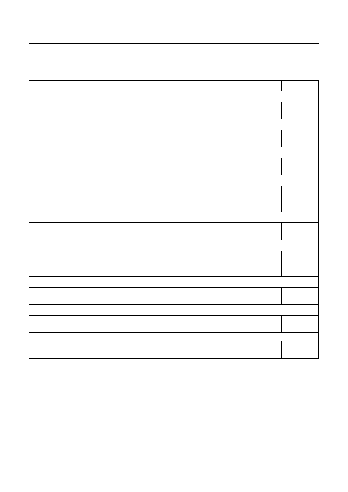
Philips Semiconductors Product specification
Universal sync generator (USG) SAA1101
SYMBOL PARAMETER PAL NTSC PAL-M SECAM UNIT N
Burst key (BK) (SECAM)
t
WBK
t
PBKCS
DURATION OF VERTICAL BLANKING
− SECAM1 −−−note 2 −−
− SECAM2 −−−note 3 −−
Clamp pulse (CLP)
t
WCLP
t
PCSCLP
Horizontal drive (HD)
t
WHD
t
PHDCS
− repetition period 64 63.56 63.56 64 µs −
chroma pulse width −−−7.2 µs36
CS to chroma delay −−−1.6 µs8
clamp pulse width 2.4 2.38 2.38 2.4 µs12
CS to CLP delay 1.6 1.59 1.59 1.6 µs8
pulse width 7.2 7.15 7.15 7.2 µs36
CS to HD delay 0.8 0.79 0.79 0.8 µs4
Vertical drive (VD)
− VD duration 10 6 6 10 H −
t
PVDCS
CS to VD delay 1.6 1.59 1.59 1.6 µs8
White measurement pulse (WMP)
− pulse width 2.4 2.38 2.38 2.4 µs12
− CS to WMP delay 34.4 34.16 34.16 34.4 µs 172
− duration of WMP 10 9 9 10 H −
POSITION OF WMP
− first half picture H163 to H173 H134 to H143 H134 to H143 H163 to H173 −−
− second half picture H475 to H485 H396 to H405 H396 to H405 H475 to H485 −−
Identification (ID)
t
WID
t
PIDCS
pulse width 12 11.12 11.12 12 µs60
CS to ID delay 1.6 1.59 1.59 1.6 µs8
POSITION OF ID
− first half picture H7 to H15 H8 to H22 H8 to H22 H7 to H15 −−
− second half picture H320 to H328 H271 to H285 H271 to H285 H320 to H328 −−
Notes to the characteristics
1. Horizontal blanking pulse width for NTSC2 can be 11.12 µs maximum
2. SECAM1, first half picture: 25H + t
3. SECAM2, first half picture: 25H + t
except H320 to H328. Second half picture: 24.5H + t
WBK
. Second half picture: 24.5H + t
WBK
WBK
.
except H7 to H15.
WBK
January 1990 13
Page 14
Philips Semiconductors Product specification
Universal sync generator (USG) SAA1101
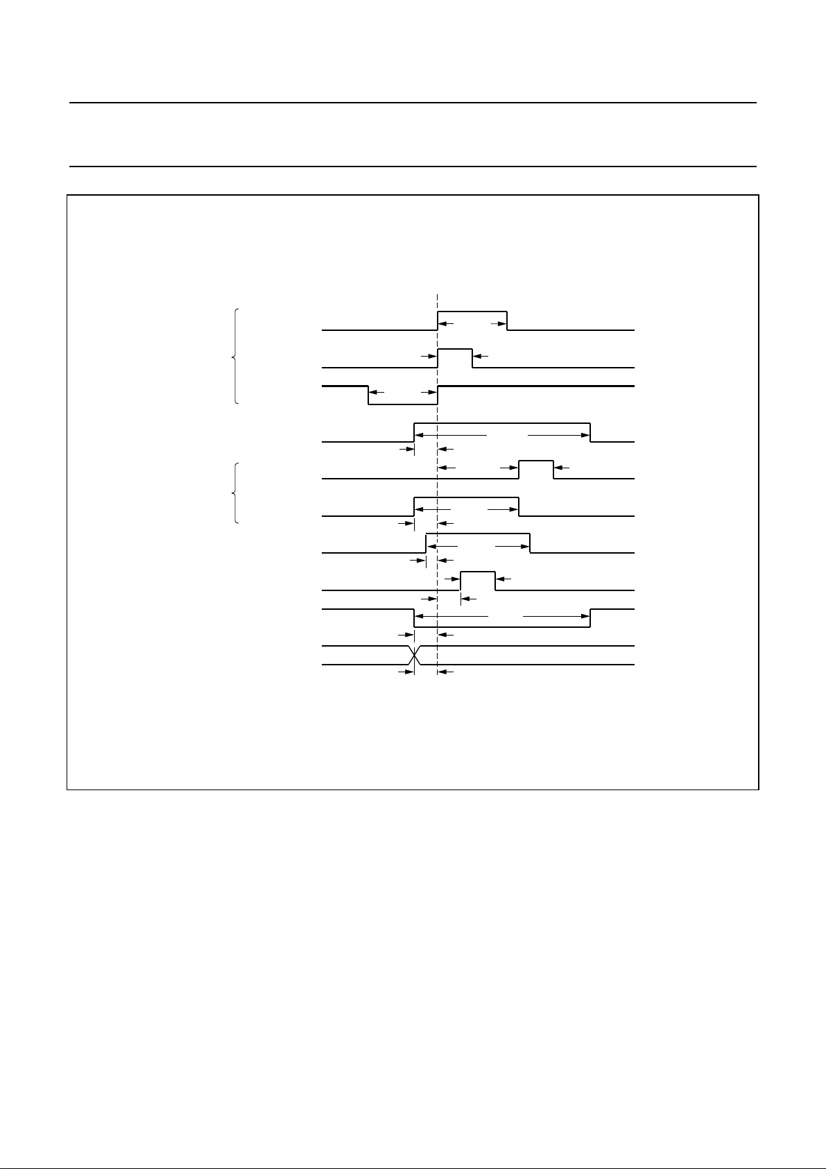
handbook, full pagewidth
composite
sync
composite
blanking
burst key/
chrominance
blanking
CS
CB
BK
HD
CLP
ID
VD
horizontal
sync pulse
equalizing pulse
serration pulse
horizontal
blanking pulse
burst key (PAL)
(SECAM)
chrominance
blanking
horizontal drive
clamp pulse
SECAM
identification
start, stop
vertical drives
t
PCBS2
t
PBKCS
t
PHDCS
t
t
PIDCS
t
WSC3
PCSCLP
t
WSC1
t
PCBSK
t
WBK
t
WHD
t
PVDCS
t
WSC2
t
WCB
t
WID
t
WCPL
t
WBK
MLA029
Fig.7 Waveform timing.
January 1990 14
Page 15
Philips Semiconductors Product specification
Universal sync generator (USG) SAA1101
PACKAGE OUTLINES
handbook, full pagewidth
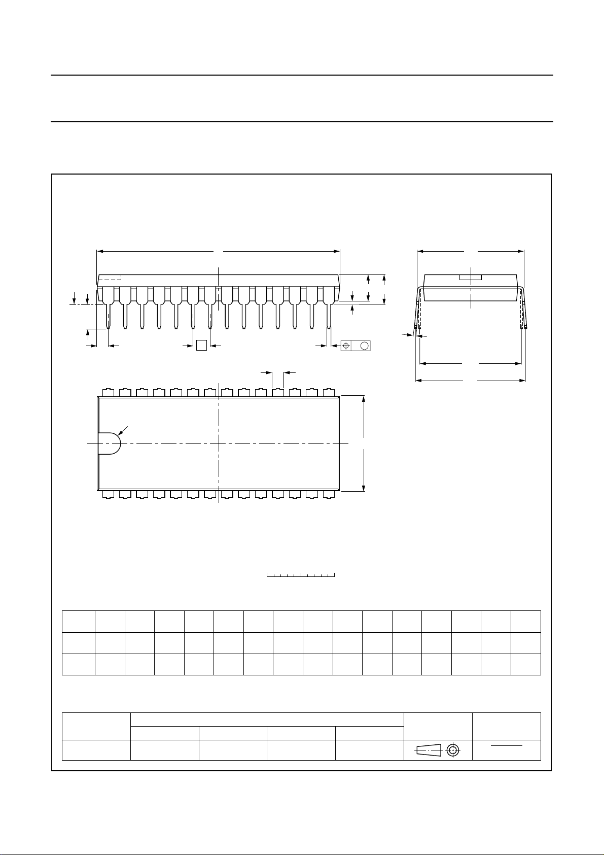
DIP28: plastic dual in-line package; 28 leads (600 mil)
SOT117-1
seating plane
L
Z
28
1
pin 1 index
D
A
2
A
A
1
e
b
w M
b
1
15
E
14
c
M
(e )
M
E
1
H
0 5 10 mm
scale
DIMENSIONS (inch dimensions are derived from the original mm dimensions)
A
A
A
UNIT
inches
Note
1. Plastic or metal protrusions of 0.25 mm maximum per side are not included.
max.
mm
OUTLINE
VERSION
SOT117-1
1 2
min.
max.
0.066
0.051
IEC JEDEC EIAJ
051G05 MO-015AH
1.7
1.3
b
b
1
0.53
0.38
0.020
0.014
0.013
0.009
REFERENCES
cD E weM
0.32
0.23
(1) (1)
36.0
35.0
1.41
1.34
January 1990 15
14.1
13.7
0.56
0.54
(1)
92-11-17
95-01-14
Z
max.
1.75.1 0.51 4.0
0.0670.20 0.020 0.16
L
3.9
3.4
EUROPEAN
PROJECTION
M
15.80
15.24
0.62
0.60
H
E
17.15
15.90
0.68
0.63
0.252.54 15.24
0.010.10 0.60
ISSUE DATE
e
1
0.15
0.13
Page 16
Philips Semiconductors Product specification
Universal sync generator (USG) SAA1101
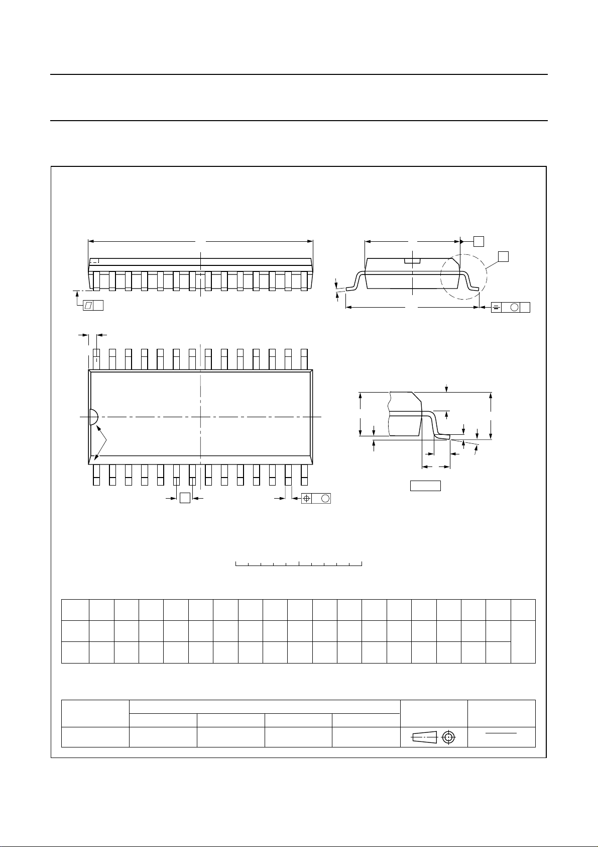
SO28: plastic small outline package; 28 leads; body width 7.5 mm
D
c
y
Z
28
pin 1 index
1
e
15
14
w M
b
p
SOT136-1
E
H
E
Q
A
2
A
1
L
p
L
detail X
(A )
A
X
v M
A
A
3
θ
0 5 10 mm
scale
DIMENSIONS (inch dimensions are derived from the original mm dimensions)
UNIT
mm
inches
Note
1. Plastic or metal protrusions of 0.15 mm maximum per side are not included.
A
max.
2.65
0.10
OUTLINE
VERSION
SOT136-1
A
0.30
0.10
0.012
0.004
A2A
1
2.45
2.25
0.096
0.089
IEC JEDEC EIAJ
075E06 MS-013AE
0.25
0.01
b
3
p
0.49
0.32
0.36
0.23
0.019
0.013
0.014
0.009
(1)E(1) (1)
cD
18.1
7.6
7.4
0.30
0.29
1.27
0.050
17.7
0.71
0.69
REFERENCES
January 1990 16
eHELLpQ
10.65
10.00
0.419
0.394
1.4
0.055
1.1
0.4
0.043
0.016
1.1
1.0
0.043
0.039
PROJECTION
0.25
0.25 0.1
0.01
0.01
EUROPEAN
ywv θ
Z
0.9
0.4
0.035
0.004
0.016
ISSUE DATE
95-01-24
97-05-22
o
8
o
0
Page 17

Philips Semiconductors Product specification
Universal sync generator (USG) SAA1101
SOLDERING
Introduction
There is no soldering method that is ideal for all IC
packages. Wave soldering is often preferred when
through-hole and surface mounted components are mixed
on one printed-circuit board. However, wave soldering is
not always suitable for surface mounted ICs, or for
printed-circuits with high population densities. In these
situations reflow soldering is often used.
This text gives a very brief insight to a complex technology.
A more in-depth account of soldering ICs can be found in
our
“IC Package Databook”
(order code 9398 652 90011).
DIP
SOLDERING BY DIPPING OR BY WAVE
The maximum permissible temperature of the solder is
260 °C; solder at this temperature must not be in contact
with the joint for more than 5 seconds. The total contact
time of successive solder waves must not exceed
5 seconds.
The device may be mounted up to the seating plane, but
the temperature of the plastic body must not exceed the
specified maximum storage temperature (T
stg max
). If the
printed-circuit board has been pre-heated, forced cooling
may be necessary immediately after soldering to keep the
temperature within the permissible limit.
R
EPAIRING SOLDERED JOINTS
Apply a low voltage soldering iron (less than 24 V) to the
lead(s) of the package, below the seating plane or not
more than 2 mm above it. If the temperature of the
soldering iron bit is less than 300 °C it may remain in
contact for up to 10 seconds. If the bit temperature is
between 300 and 400 °C, contact may be up to 5 seconds.
SO
REFLOW SOLDERING
Reflow soldering techniques are suitable for all SO
packages.
Several techniques exist for reflowing; for example,
thermal conduction by heated belt. Dwell times vary
between 50 and 300 seconds depending on heating
method. Typical reflow temperatures range from
215 to 250 °C.
Preheating is necessary to dry the paste and evaporate
the binding agent. Preheating duration: 45 minutes at
45 °C.
AVE SOLDERING
W
Wave soldering techniques can be used for all SO
packages if the following conditions are observed:
• A double-wave (a turbulent wave with high upward
pressure followed by a smooth laminar wave) soldering
technique should be used.
• The longitudinal axis of the package footprint must be
parallel to the solder flow.
• The package footprint must incorporate solder thieves at
the downstream end.
During placement and before soldering, the package must
be fixed with a droplet of adhesive. The adhesive can be
applied by screen printing, pin transfer or syringe
dispensing. The package can be soldered after the
adhesive is cured.
Maximum permissible solder temperature is 260 °C, and
maximum duration of package immersion in solder is
10 seconds, if cooled to less than 150 °C within
6 seconds. Typical dwell time is 4 seconds at 250 °C.
A mildly-activated flux will eliminate the need for removal
of corrosive residues in most applications.
R
EPAIRING SOLDERED JOINTS
Fix the component by first soldering two diagonallyopposite end leads. Use only a low voltage soldering iron
(less than 24 V) applied to the flat part of the lead. Contact
time must be limited to 10 seconds at up to 300 °C. When
using a dedicated tool, all other leads can be soldered in
one operation within 2 to 5 seconds between
270 and 320 °C.
Reflow soldering requires solder paste (a suspension of
fine solder particles, flux and binding agent) to be applied
to the printed-circuit board by screen printing, stencilling or
pressure-syringe dispensing before package placement.
January 1990 17
Page 18
Philips Semiconductors Product specification
Universal sync generator (USG) SAA1101
DEFINITIONS
Data sheet status
Objective specification This data sheet contains target or goal specifications for product development.
Preliminary specification This data sheet contains preliminary data; supplementary data may be published later.
Product specification This data sheet contains final product specifications.
Limiting values
Limiting values given are in accordance with the Absolute Maximum Rating System (IEC 134). Stress above one or
more of the limiting values may cause permanent damage to the device. These are stress ratings only and operation
of the device at these or at any other conditions above those given in the Characteristics sections of the specification
is not implied. Exposure to limiting values for extended periods may affect device reliability.
Application information
Where application information is given, it is advisory and does not form part of the specification.
LIFE SUPPORT APPLICATIONS
These products are not designed for use in life support appliances, devices, or systems where malfunction of these
products can reasonably be expected to result in personal injury. Philips customers using or selling these products for
use in such applications do so at their own risk and agree to fully indemnify Philips for any damages resulting from such
improper use or sale.
January 1990 18
 Loading...