

Page 1

INTEGRATED CIRCUITS
DATA SH EET
SAA1064
4-digit LED-driver with I
interface
Product specification
File under Integrated Circuits, IC01
2
C-Bus
February 1991
Page 2
Philips Semiconductors Product specification
4-digit LED-driver with I2C-Bus interface
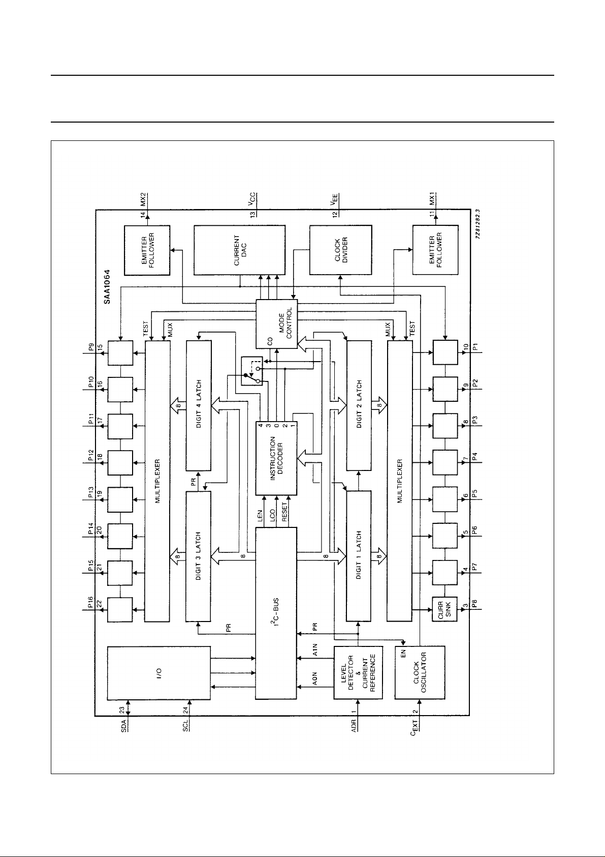
GENERAL DESCRIPTION
The LED-driver is a bipolar integrated circuit made in an
I2L compatible 18 volts process. The circuit is especially
designed to drive four 7-segment LED displays with
decimal point by means of multiplexing between two pairs
of digits. It features an I2C-Bus slave transceiver interface
with the possibility to program four different SLAVE
ADDRESSES, a POWER RESET flag, 16 current sink
OUTPUTS, controllable by software up to 21 mA, two
multiplex drive outputs for common anode segments, an
on-chip multiplex oscillator, control bits to select static,
dynamic and blank mode, and one bit for segment test.
QUICK REFERENCE DATA
PARAMETER CONDITIONS SYMBOL MIN. TYP. MAX. UNIT
Supply voltage V
Supply current all outputs OFF V
Total power dissipation
24-lead DIL (SOT101B) P
24-lead DIL SO (SOT137A) P
Operating ambient
temperature range T
= 0 V V
EE
= 5 V I
CC
CC
CC
tot
tot
amb
(1)
SAA1064
4.5 5 15 V
7 9.5 14 mA
−−1000 mW
−−500 mW
−40 − +85 °C
Note
1. The positive current is defined as the conventional current flow into a device (sink current).
PACKAGE OUTLINE
SAA1064: 24-lead DIL; plastic with internal heat spreader (SOT101B); SOT101-1; 1996 August 30.
SAA1064T: 24-lead mini-pack; plastic (SO-24; SOT137A); SOT137-1; 1996 August 30.
February 1991 2
Page 3
Philips Semiconductors Product specification
4-digit LED-driver with I2C-Bus interface
SAA1064
February 1991 3
Fig.1 Block diagram.
Page 4
Philips Semiconductors Product specification
4-digit LED-driver with I2C-Bus interface
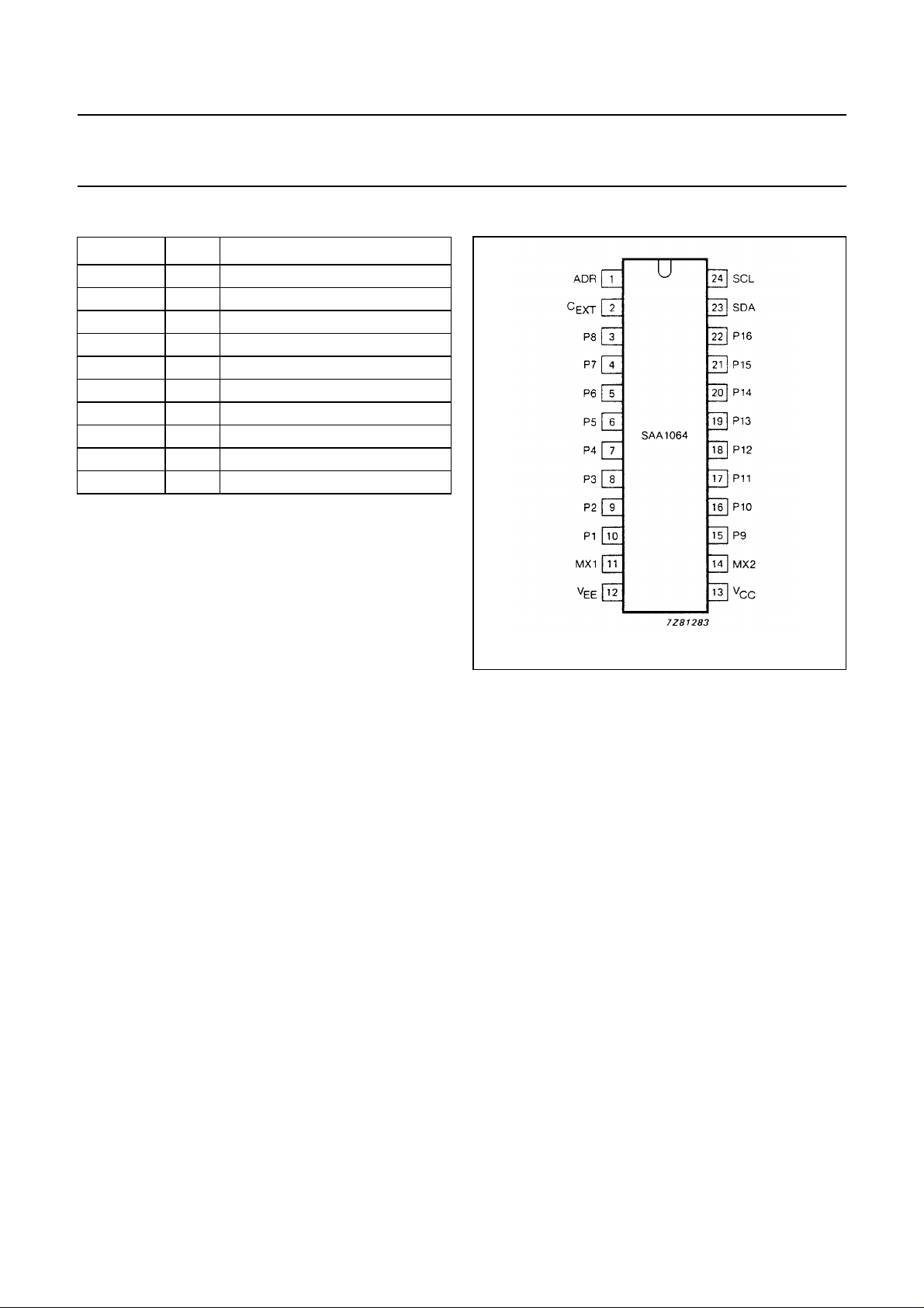
PINNING
SYMBOL PIN DESCRIPTION
2
ADR 1 I
C
EXT
2 external control
P8 to P1 3-10 segment output
MX1 11 multiplex output
V
EE
V
CC
12 ground
13 positive supply
MX2 14 multiplex output
P9 to P16 15-22 segment output
SDA 23 I
SCL 24 I
C-Bus slave address input
2
C-Bus serial data line
2
C-Bus serial clock line
SAA1064
Fig.2 Pinning diagram.
February 1991 4
Page 5
Philips Semiconductors Product specification
4-digit LED-driver with I2C-Bus interface
FUNCTIONAL DESCRIPTION
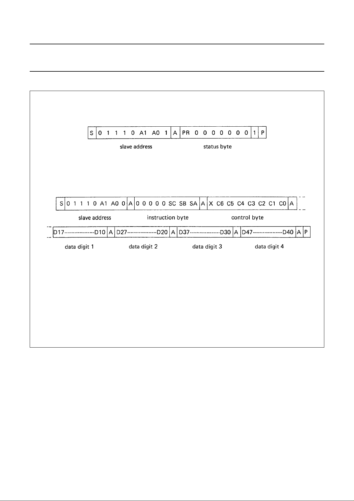
a. READ mode.
SAA1064
b. WRITE mode.
S = start condition A1, A0 = programmable address bits
P = stop condition SC SB SA = subaddress bits
A = acknowledge C6 to C0 = control bits
X = don’t care PR = POWER RESET flag
Fig.3 I2C-Bus format.
Address pin ADR
Four different slave addresses can be chosen by connecting ADR either to V
the corresponding valid addresses HEX 70, 72, 74 and 76 for writing and 71, 73, 75 and 77 for reading. All other
addresses cannot be acknowledged by the circuit.
3/8 VCC, 5/8 VCCor VCC. This results in
EE,
February 1991 5
Page 6

Philips Semiconductors Product specification
4-digit LED-driver with I2C-Bus interface
Status byte
Only one bit is present in the status byte, the POWER RESET flag. A logic 1 indicates the occurence of a power failure
since the last time it was read out. After completion of the READ action this flag will be set to logic 0.
Subaddressing
The bits SC, SB and SA form a pointer and determine to which register the data byte following the instruction byte will
be written. All other bytes will then be stored in the registers with consecutive subaddresses. This feature is called
Auto-Increment (AI) of the subaddress and enables a quick initialization by the master.
The subaddress pointer will wrap around from 7 to 0.
The subaddresses are given as follows:
SC SB SA SUB-ADDRESS FUNCTION
0 0 0 00 control register
0 0 1 01 digit 1
0 1 0 02 digit 2
0 1 1 03 digit 3
1 0 0 04 digit 4
1 0 1 05 reserved, not used
1 1 0 06 reserved, not used
1 1 1 07 reserved, not used
SAA1064
Control bits (see Fig.4)
The control bits C0 to C6 have the following meaning:
C0 = 0 static mode, i.e. continuous display of digits 1 and 2
C0 = 1 dynamic mode, i.e. alternating display of digit 1 + 3 and 2 + 4
C1 = 0/1 digits 1 + 3 are blanked/not blanked
C2 = 0/1 digits 2 + 4 are blanked/not blanked
C3 = 1 all segment outputs are switched-on for segment test
C4 = 1 adds 3 mA to segment output current
C5 = 1 adds 6 mA to segment output current
C6 = 1 adds 12 mA to segment output current
Note
1. At a current determined by C4, C5 and C6.
Data
A segment is switched ON if the corresponding data bit is logic 1. Data bits D17 to D10 correspond with digit 1, D27 to
D20 with digit 2, D37 to D30 with digit 3 and D47 to D40 with digit 4.
The MSBs correspond with the outputs P8 and P16, the LSBs with P1 and P9. Digit numbers 1 to 4 are equal to their
subaddresses (hex) 1 to 4.
(1)
February 1991 6
Page 7

Philips Semiconductors Product specification
4-digit LED-driver with I2C-Bus interface
SDA, SCL
The SDA and SCL I/O meet the I2C-Bus specification. For protection against positive voltage pulses on these inputs
voltage regulator diodes are connected to VEE. This means that normal line voltage should not exceed 5,5 volt. Data will
be latched on the positive-going edge of the acknowledge related clock pulse.
Power-on reset
The power-on reset signal is generated internally and sets all bits to zero, resulting in a completely blanked display. Only
the POWER RESET flag is set.
External Control (C
With a capacitor connected to pin 2 the multiplex frequency can be set (see Fig.5). When static this pin can be connected
to V
or VCCor left floating since the oscillator will be switched off.
EE
Segment outputs
The segment outputs P1 to P16 are controllable current-sink sources. They are switched on by the corresponding data
bits and their current is adjusted by control bits C4, C5 and C6.
Multiplex outputs
The multiplex outputs MX1 and MX2 are switched alternately in dynamic mode with a frequency derived from the
clock-oscillator. In static mode MX1 is switched on. The outputs consist of an emitter-follower, which can be used to drive
the common anodes of two displays directly provided that the total power dissipation of the circuit is not exceeded. If this
occurs external transistors should be connected to pins 11 and 14 as shown in Fig.5.
EXT
)
SAA1064
February 1991 7
Page 8

Philips Semiconductors Product specification
4-digit LED-driver with I2C-Bus interface
RATINGS
Limiting values in accordance with the Absolute Maximum System (IEC 134)
PARAMETER CONDITIONS SYMBOL MIN. MAX. UNIT
Supply voltage (pin 13) V
Supply current (pin 13) I
Total power dissipation
24-lead DIL (SOT101B) P
24-lead SO (SO137A) P
SDA, SCL voltages V
Voltages ADR-MX1 and MX2-P16 V
Input/output current all pins outputs OFF ± I
Operating ambient
temperature range T
Storage temperature range T
THERMAL RESISTANCE
From crystal to ambient
24-lead DIL R
24-lead SO (on ceramic substrate) R
24-lead SO (on printed circuit board) R
= 0 V V
EE
= 0 V V
EE
= 0 V V
EE
CC
CC
tot
tot
23, 24
1-11
I/O
amb
stg
, V
14-22
SAA1064
−0.5 18 V
−50 200 mA
1000 mW
500 mW
−0.5 5.9 V
−0.5 VCC+ 0.5 V
− 10 mA
−40 +85 °C
−55 +150 °C
th j-a
th j-a
th j-a
35 K/W
75 K/W
105 K/W
February 1991 8
Page 9

Philips Semiconductors Product specification
4-digit LED-driver with I2C-Bus interface
CHARACTERISTICS
= 5 V; T
V
CC
Supply
Supply voltage (pin 13) V
Supply current all outputs OFF
Power dissipation all outputs OFF P
SDA; SCL (pins 23 and 24)
Input voltages V
Logic input voltage LOW V
Logic input voltage HIGH V
Input current LOW V
Input current HIGH V
SDA
Logic output voltage LOW I
Output sink current I
Address input (pin 1)
Input voltage
programmable address bits:
A0 = 0; A1 = 0 V
A0 = 1; A1 = 0 V
A0 = 0; A1 = 1 V
A0 = 1; A1 = 1 V
Input current LOW V
Input current HIGH V
External control (C
Switching level input
Input voltage LOW V
Input voltage HIGH V
Input current V
= 25 °C; voltages are referenced to ground (V
amb
PARAMETER CONDITIONS SYMBOL MIN. TYP. MAX. UNIT
VCC= 5 V I
= V
EXT
) pin 2
23,24
23,24
= 3 mA V
O
1
1
2
V
2
EE
= V
CC
= V
EE
= V
CC
= 2 V I
= 4 V I
CC
−I
I
IH
SDA
−I
I
1
2
2
CC
d
23,24
IL(L)
IH(L)
IL
OL(L)
1
1
1
1
1
IL
IH
SAA1064
0 V); unless otherwise specified
EE =
4,5 5,0 15 V
7,0 9,5 14,0 mA
− 50 − mW
0 − 5,5 V
−−1,5 V
3,0 −−V
−−10 µA
−−10 µA
−−0,4 V
3 −−mA
V
EE
5/16V
9/16V
13/16V
−−10 µA
−−10 µA
−−V
VCC−1,5 −−V
−140 −160 −180 µA
140 160 180 µA
− 3/16V
3/8V
CC
5/8V
CC
− V
CC
CC
CC
7/16V
11/16V
CC
−3,3 V
CC
CC
CC
CC
V
V
V
V
February 1991 9
Page 10

Philips Semiconductors Product specification
4-digit LED-driver with I2C-Bus interface
SAA1064
PARAMETER CONDITIONS SYMBOL MIN. TYP. MAX. UNIT
Segment outputs
(P8 to P1; pins 3 to 10)
P9 to P16; pins 15 to 22)
Output voltages I
Output leakage current HIGH V
= 15 mA V
O
= VCC= 15 V I
O
LO
O
−−0.5 V
−−±10 µA
Output current LOW
All control bits (C4, C5
and C6) are HIGH V
= 5 V I
OL
OL
17.85 21 25.2 mA
Contribution of:
control bit C4 I
control bit C5 I
control bit C6 I
O
O
O
2.55 3.0 3.6 mA
5.1 6.0 7.2 mA
10.2 12.0 14.4 mA
Relative segment output
current accuracy
with respect to highest value ∆I
O
−−7.5 %
Multiplex 1 and 2 (pins 11
and 14)
Maximum output voltage
(when ON) −I
= 50 mA V
MPX
MPX
VCC−1.5 −−V
Maximum output current HIGH
(when ON) V
= 2 V −I
MPX
MPX
50 − 110 mA
Maximum output current LOW
(when OFF) V
Multiplex output period C
= 2 V +I
O
= 2.7 nF T
EXT
MPX
MPX
50 70 110 µA
5 − 10 ms
Multiplexed duty factor − 48.4 − %
* Value to be fixed.
February 1991 10
Page 11

Philips Semiconductors Product specification
4-digit LED-driver with I2C-Bus interface
SAA1064
Fig.4 Timing diagram.
February 1991 11
Page 12

Philips Semiconductors Product specification
4-digit LED-driver with I2C-Bus interface
APPLICATION INFORMATION
SAA1064
Fig.5 Dynamic mode application diagram.
February 1991 12
Page 13

Philips Semiconductors Product specification
4-digit LED-driver with I2C-Bus interface
SAA1064
Fig.6 Static mode application diagram.
February 1991 13
Page 14

Philips Semiconductors Product specification
4-digit LED-driver with I2C-Bus interface
SAA1064
POWER DISSIPATION
The total maximum power dissipation of the SAA1064 is made up by the following parts:
1. Maximum dissipation when none of the outputs are programmed (continuous line in Fig.7).
2. Maximum dissipation of each programmed output. The dashed line in Fig.7 visualises the dissipation when all the
segments are programmed (max. 16 in the static, and max. 32 in the dynamic mode). When less segments are
programmed one should take a proportional part of the maximum value.
3. Maximum dissipation of the programmed segment drivers which can be expressed as:
P
= VO× IO× N.
add
Where: P
= The additional power dissipation of the segment drivers
add
V
= The low state segment driver output voltage
O
I
= The programmed segment output current
O
N = The number of programmed segments in the static mode, or half the number of
programmed segment drivers in the dynamic mode.
Under no conditions the total maximum dissipation (500 mW for the SO and 1000 mW for the DIL package) should be
exceeded.
Example: V
=5 V
CC
V
= 0.25 V
O
I
= 12 mA
O
24 programmed segments in dynamic mode
P
=P1+P2+P
tot
3
= 75 mW + (50 * 24/32) mW + (0.25 * 12.10−3* 12) mW
= 148.5 mW
February 1991 14
Page 15

Philips Semiconductors Product specification
4-digit LED-driver with I2C-Bus interface
750
handbook, full pagewidth
dissipation
(mW)
500
250
SAA1064
MEA104
(1)
(2)
0
0 2.5 12.5
(1) All outputs programmed (no segment current sink).
(2) Outputs not programmed.
Fig.7 SAA1064 power dissipation as a function of supply voltage.
7.55.0
10.0
VCC (V)
15.0
February 1991 15
Page 16

Philips Semiconductors Product specification
4-digit LED-driver with I2C-Bus interface
PACKAGE OUTLINES
DIP24: plastic dual in-line package; 24 leads (600 mil)
D
seating plane
L
Z
24
e
b
SAA1064
SOT101-1
M
E
A
2
A
A
1
w M
b
1
13
c
(e )
1
M
H
pin 1 index
1
0 5 10 mm
DIMENSIONS (inch dimensions are derived from the original mm dimensions)
A
A
A
UNIT
inches
Note
1. Plastic or metal protrusions of 0.25 mm maximum per side are not included.
max.
mm
OUTLINE
VERSION
SOT101-1
1 2
min.
max.
1.7
1.3
0.066
0.051
IEC JEDEC EIAJ
051G02 MO-015AD
b
b
1
0.53
0.38
0.021
0.015
0.32
0.23
0.013
0.009
REFERENCES
cD E e M
32.0
31.4
1.26
1.24
12
scale
14.1
13.7
0.56
0.54
E
(1)(1)
e
L
3.9
3.4
EUROPEAN
PROJECTION
M
15.80
15.24
0.62
0.60
E
17.15
15.90
0.68
0.63
1
0.15
0.13
H
w
0.252.54 15.24
0.010.10 0.60
ISSUE DATE
92-11-17
95-01-23
Z
max.
2.25.1 0.51 4.0
0.0870.20 0.020 0.16
(1)
February 1991 16
Page 17

Philips Semiconductors Product specification
4-digit LED-driver with I2C-Bus interface
SO24: plastic small outline package; 24 leads; body width 7.5 mm
D
c
y
Z
24
13
SAA1064
SOT137-1
E
H
E
A
X
v M
A
pin 1 index
1
e
0 5 10 mm
DIMENSIONS (inch dimensions are derived from the original mm dimensions)
mm
A
max.
2.65
0.10
A1A2A
0.30
2.45
0.10
2.25
0.012
0.096
0.004
0.089
0.25
0.01
b
3
p
0.49
0.32
0.36
0.23
0.019
0.013
0.014
0.009
UNIT
inches
Note
1. Plastic or metal protrusions of 0.15 mm maximum per side are not included.
(1)E(1) (1)
cD
15.6
15.2
0.61
0.60
12
w M
b
p
scale
eHELLpQ
7.6
1.27
7.4
0.30
0.050
0.29
10.65
10.00
0.419
0.394
A
1.4
0.055
Q
2
A
1
detail X
1.1
1.1
0.4
0.043
0.016
1.0
0.043
0.039
0.25
0.01
L
p
L
(A )
0.25 0.1
0.01
A
3
θ
ywv θ
Z
0.9
0.4
0.035
0.004
0.016
o
8
o
0
OUTLINE
VERSION
SOT137-1
IEC JEDEC EIAJ
075E05 MS-013AD
REFERENCES
February 1991 17
EUROPEAN
PROJECTION
ISSUE DATE
95-01-24
97-05-22
Page 18

Philips Semiconductors Product specification
4-digit LED-driver with I2C-Bus interface
SOLDERING
Introduction
There is no soldering method that is ideal for all IC
packages. Wave soldering is often preferred when
through-hole and surface mounted components are mixed
on one printed-circuit board. However, wave soldering is
not always suitable for surface mounted ICs, or for
printed-circuits with high population densities. In these
situations reflow soldering is often used.
This text gives a very brief insight to a complex technology.
A more in-depth account of soldering ICs can be found in
“IC Package Databook”
our
DIP
SOLDERING BY DIPPING OR BY WAVE
The maximum permissible temperature of the solder is
260 °C; solder at this temperature must not be in contact
with the joint for more than 5 seconds. The total contact
time of successive solder waves must not exceed
5 seconds.
The device may be mounted up to the seating plane, but
the temperature of the plastic body must not exceed the
specified maximum storage temperature (T
printed-circuit board has been pre-heated, forced cooling
may be necessary immediately after soldering to keep the
temperature within the permissible limit.
R
EPAIRING SOLDERED JOINTS
Apply a low voltage soldering iron (less than 24 V) to the
lead(s) of the package, below the seating plane or not
more than 2 mm above it. If the temperature of the
soldering iron bit is less than 300 °C it may remain in
contact for up to 10 seconds. If the bit temperature is
between 300 and 400 °C, contact may be up to 5 seconds.
SO
REFLOW SOLDERING
Reflow soldering techniques are suitable for all SO
packages.
(order code 9398 652 90011).
). If the
stg max
SAA1064
Several techniques exist for reflowing; for example,
thermal conduction by heated belt. Dwell times vary
between 50 and 300 seconds depending on heating
method. Typical reflow temperatures range from
215 to 250 °C.
Preheating is necessary to dry the paste and evaporate
the binding agent. Preheating duration: 45 minutes at
45 °C.
AVE SOLDERING
W
Wave soldering techniques can be used for all SO
packages if the following conditions are observed:
• A double-wave (a turbulent wave with high upward
pressure followed by a smooth laminar wave) soldering
technique should be used.
• The longitudinal axis of the package footprint must be
parallel to the solder flow.
• The package footprint must incorporate solder thieves at
the downstream end.
During placement and before soldering, the package must
be fixed with a droplet of adhesive. The adhesive can be
applied by screen printing, pin transfer or syringe
dispensing. The package can be soldered after the
adhesive is cured.
Maximum permissible solder temperature is 260 °C, and
maximum duration of package immersion in solder is
10 seconds, if cooled to less than 150 °C within
6 seconds. Typical dwell time is 4 seconds at 250 °C.
A mildly-activated flux will eliminate the need for removal
of corrosive residues in most applications.
EPAIRING SOLDERED JOINTS
R
Fix the component by first soldering two diagonally-
opposite end leads. Use only a low voltage soldering iron
(less than 24 V) applied to the flat part of the lead. Contact
time must be limited to 10 seconds at up to 300 °C. When
using a dedicated tool, all other leads can be soldered in
one operation within 2 to 5 seconds between
270 and 320 °C.
Reflow soldering requires solder paste (a suspension of
fine solder particles, flux and binding agent) to be applied
to the printed-circuit board by screen printing, stencilling or
pressure-syringe dispensing before package placement.
February 1991 18
Page 19

Philips Semiconductors Product specification
4-digit LED-driver with I2C-Bus interface
DEFINITIONS
Data sheet status
Objective specification This data sheet contains target or goal specifications for product development.
Preliminary specification This data sheet contains preliminary data; supplementary data may be published later.
Product specification This data sheet contains final product specifications.
Limiting values
Limiting values given are in accordance with the Absolute Maximum Rating System (IEC 134). Stress above one or
more of the limiting values may cause permanent damage to the device. These are stress ratings only and operation
of the device at these or at any other conditions above those given in the Characteristics sections of the specification
is not implied. Exposure to limiting values for extended periods may affect device reliability.
Application information
Where application information is given, it is advisory and does not form part of the specification.
LIFE SUPPORT APPLICATIONS
These products are not designed for use in life support appliances, devices, or systems where malfunction of these
products can reasonably be expected to result in personal injury. Philips customers using or selling these products for
use in such applications do so at their own risk and agree to fully indemnify Philips for any damages resulting from such
improper use or sale.
SAA1064
PURCHASE OF PHILIPS I
Purchase of Philips I
components in the I2C system provided the system conforms to the I2C specification defined by
Philips. This specification can be ordered using the code 9398 393 40011.
2
C COMPONENTS
2
C components conveys a license under the Philips’ I2C patent to use the
February 1991 19
 Loading...