

Page 1

SAA1029
UNIVERSAL INDUSTRIAL LOGIC AND INTERFACE CIRCUIT
GENERAL DESCRIPTION
The SAA1029 is a universal bipolar logic and interface IC with high noise immunity and
operational stability for industrial control applications. The most fundamental industrial
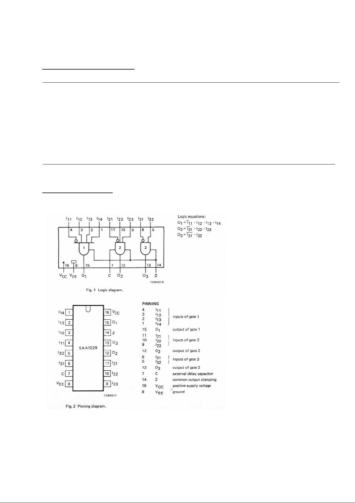
control functions can be accomplished with only one SAA1029IC. Figure 1 shows the lo gic
configuration.
The IC comprises,
(1) Gate 1 : 4-input AND gate with 1 inverted input,
(2) Gate 2 : 3-input AND gate with 1 inverted input and adjustable propagation delay,
(3) Gate 3 : 2-input AND gate with 1 inverted input.
The SAA1029 can be used as direct interface with LOCMOS (CMOS) Ics for realizing more
complex functions. Therefore, the output signal can be limited to the voltage level of the
common output claming pin Z.
The propagation delay of NAND gate 2 is adjustable from microseconds by using an external
capacitor at pin C. This makes it possible to adapt the control frequency limits to the system,
so the optimum dynamic noise » immunity can be achieved.
All the static and dynamic circuit values ( including the output voltage) are independent of the
supply voltage over a wide operating range. This allows the use of a simple unstabilized
power supply.
The output is held to the LOW state automatically during swithching on the power supply, so
a special reset pulse can be omitted.
Features
• Simple realization of the basic industrial control functions ( logic functions, timing
functions, memory functions).
• High dynamic and static noise immunity.
• High operation stability.
• Short-circut protection of inputs and outputs to both V
EE
and V
CC.
• Wide interruption results in a safe input LOW state.
• LOCMOS (CMOS) compatible.
COMSET SEMICONDUCTORS
1/1
Page 2
SAA1029
QUICK REFERENCE DATA
Supply voltage range V
Operating ambient temerature range T
Input voltage HIGH V
Output voltage HIGH (without clamping) V
Output voltage HIGH (without clamping at pin Z) V
Input current I
Quiescent supply current I
PACKAGE OUTLINE
16-lead DIL ; plastic (SOT38).
I
CC
CC
amb
IH
OH
OH
14 to 31,2V
-30 to +85°C
7,5 to 44V
13 to 30V
2,0 to (VCC –0,7)V
max. 10mA
typ. 7,8mA
COMSET SEMICONDUCTORS
2/3
Page 3

SAA1029
CHARACTERISTICS : At Tamb : -10 to +85°C/ Vcc 14V to 32V
PARAMETER CONDITIONS
SUPPLY VOLTAGE
OUTPUT CLAMPING
VOLTAGE
INPUT VOLTAGE LOW
INPUT VOLTAGE HIGH
CURRENT
CONSOMATION
INPUT CURRENT
OUTPUT VOLTAGE
HIGH
OUTPUT VOLTAGE
LOW
OUTPUT SHORTCIRCULT CURRENT
VZ=VCC-1 VZ 0 30 V
VCC :30V ICC 6,5 12
VCC :24V I
VCC :14V
-IoH :3 mA
VCC :30V
-IoL :1,6 mA
SYMB
MIN TYP MAX UNIT
VCC 14 32 V
VIL -0,15 +5 V
VIH +7,5 +44 V
m
IL :IIH
0,1 0,15 0,3
m
VoH 12 12,8 V
VoL 0,9 1,4 V
A
A
LOW SIGNAL
HIGH SIGNAL
PROPAGATION
DELAYS
GATE 2
HIGH TO LOW
LOW TO HIGH
GATE 1,2,3
HIGH TO LOW
LOW TO HIGH
Tamb :25°C
VCC24V
C :33nF
C :33nF
C :0nF
C :0nF
COMSET SEMICONDUCTORS
10SL 6
10SH 10 18
pHL 1,5 2,6 4
t
pLH 5,5 8,5 12
t
PHL 1 2,1 9
t
PLH 1 4,4 9
t
3/3
m
m
m
m
M
M
A
A
D
S
D
D
 Loading...