

Page 1

INTEGRATED CIRCUITS
SA647
Low-voltage digital IF receiver
Product specification 1998 Aug 10
Page 2
Philips Semiconductors Product specification
SA647Low-voltage digital IF receiver
DESCRIPTION
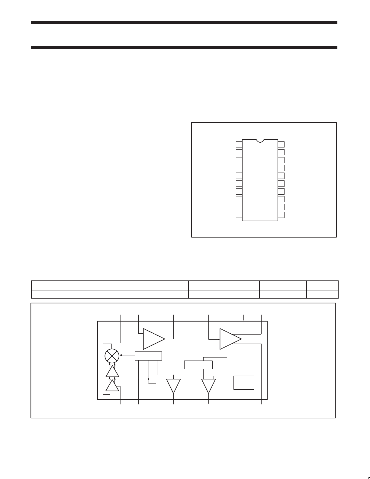
The SA647 is a low-voltage high performance monolithic digital
system with high-speed RSSI incorporating a mixer, oscillator with
buffered output, two limiting intermediate frequency amplifiers, fast
logarithmic received signal strength indicator (RSSI), voltage
regulator, RSSI op amp and power down pin. The SA647 is
available in TSSOP (thin shrink small outline package).
The SA647 was designed for portable digital communication
applications and will function down to 2.7V . The limiter amplifier has
differential outputs with 2MHz small signal bandwidth. The RSSI
output has access to the feedback pin. This enables the designer to
level adjust the outputs or add filtering.
FEA TURES
•V
= 2.7 to 5.5V
CC
•Low power receiver (5.3mA @ 3V)
•Power down mode (I
= 110µA)
CC
•Fast RSSI rise and fall times
•Extended RSSI range with temperature compensation
•RSSI op amp
•2MHz limiter small signal bandwidth
•Filter matching (1.5kΩ)
•Differential limiter output
•Oscillator buffer
•TSSOP-20 package
APPLICA TIONS
•NADC (North American Digital Cellular)
•Digital receiver systems
•Cellular radio
PIN CONFIGURATION
1
RF
IN+
2
RF
IN–
3
OSC E
4
OSC B
OSC
BUF
LIM OUT (-)
5
OUT
6
V
CC
7
RSSI
8
RSSI FB
9
P
D
10
Figure 1. Pin Configuration
20
MIX
19
IF AMP
18
IF AMP
17
IF AMP
16
IF AMP
15
GND
14
LIM
13
LIM
12
LIM
11
LIM OUT (+)
OUT
DECOUP
IN
DECOUP
OUT
IN
DECOUP
DECOUP
SR01456
ORDERING INFORMATION
DESCRIPTION TEMPERATURE RANGE ORDER CODE DWG #
20-Pin Plastic Thin Shrink Small Outline Package (Surface-mount) –40 to +85°C SA647DH SOT360–1
20 19 18 17 16 15 14 13 12 11
GND
IF
AMP
MIXER
OSCILLATOR
FAST RSSI
+–
EB
123 45678 910
V
CC
Figure 2. Block Diagram
+–
LIMITER
POWER
DOWN
SR01727
1998 Aug 10 853–2037 19849
2
Page 3
Philips Semiconductors Product specification
SA647Low-voltage digital IF receiver
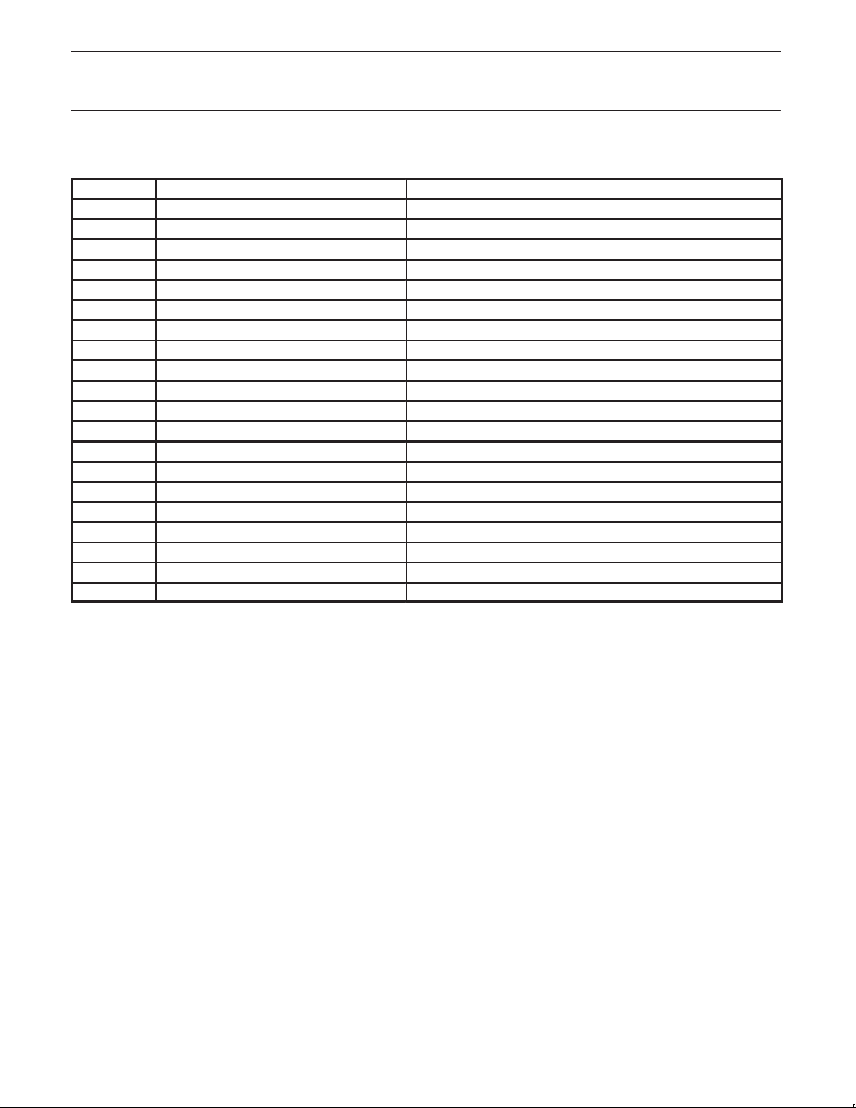
PIN DESCRIPTION
PIN NO. SYMBOL FUNCTION
1 RF
IN
2 RF BYPASS RF bypass
3 OSC
4 OSC
5 OSC
6 V
E
B
OUT Oscillator buffer output
BUF
CC
7 RSSI RSSI output
8 RSSI FB RSSI Feedback
9 P
10 LIM
11 LIM
12 LIM
13 LIM
14 LIM
D
OUT(–)
OUT(+)
DECOUP
DECOUP
IN
15 GND Ground
16 IF AMP
17 IF AMP
18 IF AMP
19 IF AMP
20 MIX
OUT
DECOUP
IN
DECOUP
OUT
RF input
Oscillator emitter
Oscillator base (input)
Supply voltage
Power Down
Limiter output (neg)
Limiter output (pos)
Limiter decoupling
Limiter decoupling
Limiter input
IF amplifier output
IF amplifier decoupling
IF amplifier input
IF amplifier decoupling
Mixer output
1998 Aug 10
3
Page 4
Philips Semiconductors Product specification
SYMBOL
PARAMETER
TEST CONDITIONS
UNITS
A
V
SA647Low-voltage digital IF receiver
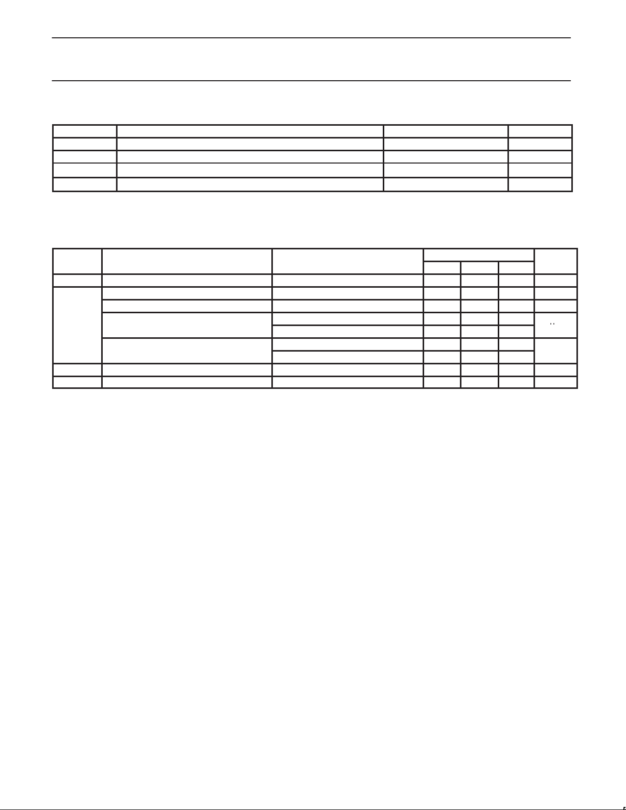
ABSOLUTE MAXIMUM RATINGS
SYMBOL PARAMETER RATING UNITS
V
CC
V
IN
T
STG
T
A
NOTE: Thermal impedance (θJA) = 135°C/W
DC ELECTRICAL CHARACTERISTICS
VCC = +3.0V , TA = 25°C; unless otherwise stated.
V
CC
I
CC
τ
on
τ
off
Supply voltage -0.3 to +6.0 V
Voltage applied to any other pin -0.3 to (VCC + 0.3) V
Storage temperature range -65 to +150
Operating ambient temperature range -40 to +85
°C
°C
LIMITS
MIN TYP MAX
Power supply voltage range 2.7 5.5 V
DC current drain 4 5.3 7 mA
Standby Pin 9 = LOW 0.11 mA
Input current Pin 9 = LOW -10 10
Pin 9 = HIGH -10 10
Input level Pin 9 = LOW 0 0.3V
Pin 9 = HIGH 0.7 V
CC
V
Power–up time RSSI valid (10% to 90%) 10
Power–down time RSSI valid (90% to 10%) 5
CC
CC
µ
sec
sec
1998 Aug 10
4
Page 5
Philips Semiconductors Product specification
SYMBOL
PARAMETER
TEST CONDITIONS
UNITS
SA647Low-voltage digital IF receiver
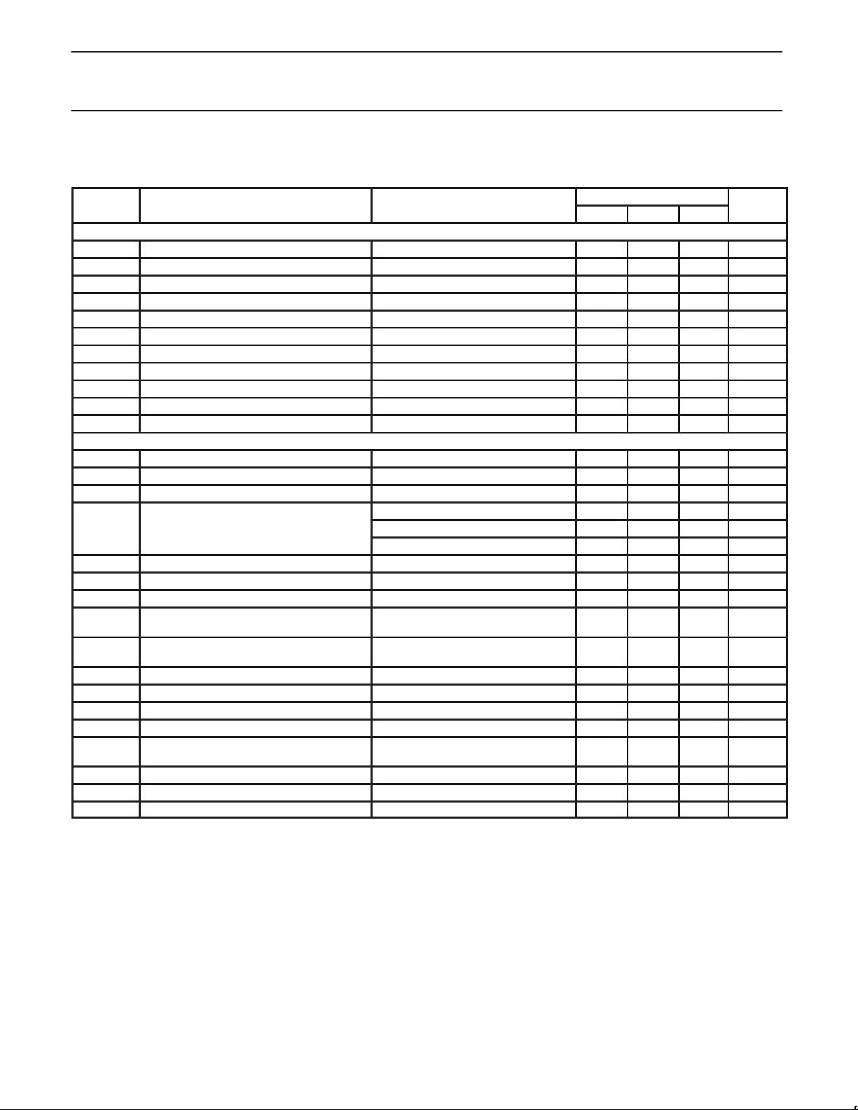
AC ELECTRICAL CHARACTERISTICS
VCC = +3.0V , Mixer input freq = 110.52MHz, LO input freq = 109.92MHz, TA = 25°C; unless otherwise stated.
LIMITS
MIN TYP MAX
Mixer/Osc section
f
IN
f
OSC
NF Noise figure at 110.52MHz Matched input and output 50Ω 4.5 dB
IIP3 Third-order input intercept point Matched input and output to 50Ω -29.5 dBm
G
CP
R
C
R
OUT
I
SOL
IF section
IF
BW
Input signal frequency 200 MHz
Crystal oscillator frequency 200 MHz
Conversion power gain Matched input and output to 50Ω 17 20 23 dB
Mixer input resistance at 110.52 MHz 670 Ω
IN
Mixer input capacitance at 110.52 MHz 3.0 pF
IN
Mixer output resistance at 600 kHz 1.5 kΩ
Mixer RF to LO isolation 32 dB
Buffered LO output level, DC coupled 10kII3.9pF load 110 230 320 mV
External input level f = 110.52 MHz at Pin 4 250 mV
IF amp power gain
Matched input and output 50W
30 36 dB
Limiter power gain 51 60 dB
IF amp bandwidth 2 MHz
RSSI output Input power level = -113dBm, Pin 1 0.30 V
Input power level = -68dBm, Pin 1 1.00 V
Input power level = -29dBm, Pin 1 1.55 V
RSSI range 85 dB
RSSI accuracy ±1.5 dB
RSSI ripple 30 mV
RSSI speed – (Rise Time)
Input @ Pin 1 No filter
RSSI speed – (Fall time)
Input @ Pin 1
No filter 25 µs
5 µs
IF input impedance 1.5 kΩ
IF output impedance 1.5 kΩ
Limiter input impedance 1.5 kΩ
Limiter output impedance (Pin 10, Pin 11) 230 Ω
Limiter output (each pin)
Output load is 1.5K in parallel with 30
pF to GND each pin
240 350 420 mV
Limiter output DC level 1.27 V
Differential output matching ±5 mV
Limiter output offset 0.09 V
P–P
P–P
P–P
P–P
1998 Aug 10
5
Page 6

Philips Semiconductors Product specification
SA647Low-voltage digital IF receiver
CIRCUIT DESCRIPTION
Mixer
The mixer has a single–ended input. The input impedance is 670Ω
in parallel with a 3.0pF cap at 110.52MHz RF. The mixer output can
drive a 1500Ω ceramic filter without any matching required.
Oscillator and Buffer
The on-board oscillator supplies the signal for the mixer
down-conversion. The internally biased transistor can be configured
as a Colpitts or Butler overtone crystal oscillator. The transistor’s
bias current can be increased if desired by adding a shunt resistor
from Pin 3 to ground. The oscillator’s buffered output (Pin 5) can be
used as a feedback signal to lock the oscillator to an appropriate
reference.
IF Amplifier and IF Limiter
The IF strip provides more than 96dB of power gain for the down
converted signal. Its bandwidth is 2MHz. The input and output
impedance of the IF amplifier and the input impedance of the IF
limiter are set to 1500Ω. A second filter is connected between the IF
amplifier and the limiter for improved channel selectivity and
reduced instability . The overall gain can be reduced if desired by
adding an external attenuator after the IF amplifier The differential
limiter outputs (Pins 10 and 11) are available for demodulator
circuits.
RSSI
The received signal strength indicator provides a linear voltage
indication of the received signal strength in dB for a typical range of
85dB. The response time to a change in input signal is less than a
few microseconds and the delay is kept to a minimum because of
the use of a minimum phase shift circuit. Because of the speed of
the RSSI circuit, the RSSI rise and fall time will be dominated by the
bandwidth of the external bandpass filter that is placed between the
mixer and the IF. Since the RSSI function requires the signal to
propagate through the whole IF strip, and the rise and fall time of the
filters are inversely proportional to their bandwidth, there is a
trade-off between channel selectivity and RSSI response.
Therefore, it is recommended that all channel selection filters be
placed before the IF strip, just after the mixer. This will make the
delay of the RSSI independent of the mixer input signal amplitude.
Also, a 6dB insertion loss between the IF and limiter sections (Pins
16 and 14) will give optimum flatness of RSSI versus mixer input
signal.
The RSSI curve is temperature compensated and in addition is
designed for improved consistency from unit to unit.
DC Power Supply
The IC is designed for operation between 2.7 and 5.5V. A power
supply dependent biasing scheme is used in the mixers to benefit
from the large headroom available at higher V
CC
s.
1998 Aug 10
6
Page 7
Philips Semiconductors Product specification
SA647Low-voltage digital IF receiver
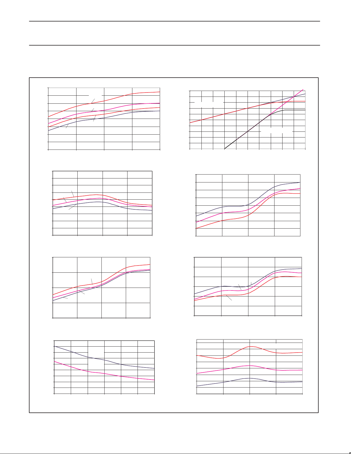
PERFORMANCE CHARACTERISTICS
VCC = +3.0V , Mixer input freq = 110.52MHz, LO input freq = 109.92MHz, TA = 25°C; unless otherwise stated.
7.00
6.50
6.00
5.50
5.00
4.50
Current (mA)
4.00
3.50
3.00
–40 0 25 70 85
24.0
23.0
22.0
21.0
20.0
19.0
Gain (dB)
18.0
17.0
16.0
15.0
5.5
5.0
4.5
Noise Figure (dB)
4.0
3.5
550
500
450
400
350
300
250
LO Output (mVp–p)
200
150
100
Supply Current vs Temperature and Supply Voltage
5.5V
3.8V
3.0V
2.7V
Temperature (°C)
Mixer Gain vs Temperature and Supply Voltage
5.5V
3.0V
2.7V
–40 0 25 70 85
Mixer Noise Figure vs Temperature and Supply Voltage
2.7V
–40 0 25 70 85
0
1 2.2 3 3.9 4.7 5.6
Temperature (°C)
5.5V
3.0V
Temperature (°C)
LO Buffer Output with Load Variation
5.1KW
10KW
Capacitor Load (pF)
Mixer 3rd Order Intercept and Compression vs Input Power
0
–10
–20
Fund. Product
–30
–40
–50
–60
–70
Output Power (dBm)
–80
–90
–100
–75 –70 –65 –60 –55 –50 –45 –40 –35 –30 –25
Mixer 3rd Order Input Intercept Point vs Temperature
–25
–26
–27
–28
–29
IP3 (dBm)
–30
–31
–32
–33
–40 0 25 70 85
Mixer 1dB Input Compression vs Temperature and Supply Voltage
–36
–37
–38
–39
–40
Compression (dBm)
–41
–42
–40 0 25 70 85
310
290
270
250
230
210
190
LO Buffer Output (mVp–p)
170
150
LO Buffer Output vs Temperature and Supply Voltage
5.5V
3.0V
2.7V
–40 0 25 70 85
Input Power (dBm)
and Supply Voltage
2.7V
3.0V
5.5V
Temperature (°C)
3.0V
5.5V
Temperature (°C)
Temperature (°C)
3rd Order Product
2.7V
Load = 10KW 3.9pF
SR01554
1998 Aug 10
Figure 3.
7
Page 8
Philips Semiconductors Product specification
SA647Low-voltage digital IF receiver
3.4
3.2
3.0
2.8
2.6
Bandwidth (MHz)
2.4
2.2
2.0
–40 0 25 70 85
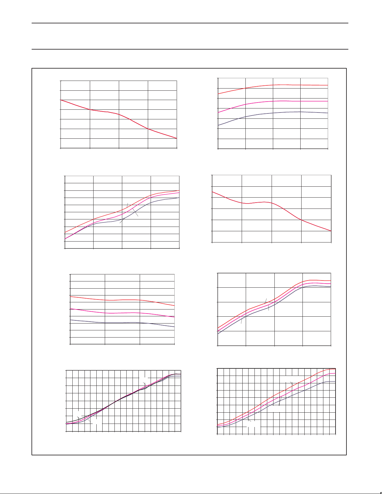
Limiter Output Offset vs Temperature and Supply Voltage
0.14
0.13
0.12
0.11
0.10
0.09
0.08
Offset (Volt)
0.07
0.06
0.05
0.04
–400 257085
65.0
64.5
64.0
63.5
63.0
Gain (dB)
62.5
62.0
61.5
61.0
60.5
60.0
–40°C
IF Bandwidth vs. Temperature
Temperature (°C)
5.5V
3.0V
2.7V
Temperature (°C)
Limiter Gain vs Temperature and Supply Voltage
5.5V
3.0V
2.7V
25 70 85
Temperature (°C)
38.5
38.0
37.5
37.0
36.5
Gain (dB)
36.0
35.5
35.0
2.8
2.6
2.4
2.2
2.0
Bandwidth (MHz)
1.8
1.6
–40 0 25 70 85
450
400
350
300
Output (mVp–p)
250
200
IF Gain vs Temperature and Supply Voltage
5.5V
3.0V
2.7V
–40 0 25 70 85
Limiter Bandwidth vs Temperature
Limiter Output vs Temperature and Supply Voltage
2.7V
–400 257085
Temperature (°C)
Temperature (°C)
5.5V
3.0V
Temperature (°C)
RSSI (Volt)
1998 Aug 10
1.6
1.4
1.2
1.0
0.8
0.6
85°C
0.4
0.2
0.0
–118 –108 –98 –88 –78 –68 –58 –48 –38 –28
RSSI vs Temperature
25°C
–40°C
RF Input (dBm)
Figure 4.
8
1.80
1.60
1.40
1.20
1.00
0.80
RSSI (Volt)
0.60
0.40
0.20
0.00
–118 –108 –98 –88 –78 –68 –58 –48 –38 –28
RSSI vs Supply Voltage
5.5V
3.0V
2.7V
RF Input (dBm)
SR01555
Page 9
Philips Semiconductors Product specification
SA647Low-voltage digital IF receiver
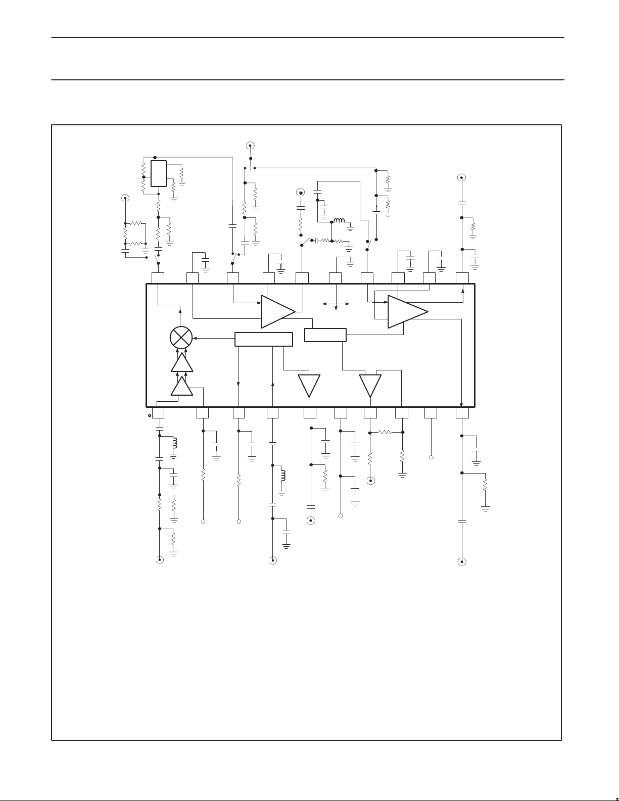
GENERAL TEST CIRCUIT DESCRIPTION
IF OR LIMITER INPUT
FLT
2
MIXER OUT
C28
R21
R29
R28
R30
R22
R23
4
R27
3
5
1
R25
C27
R24
R26
C26
C25
R18
C24
R19
C22
R20
C23
R17
C21
R16
C19
C20
L3
R15
C18
R13
R14
C17
LIMITER OUT (+)
C14
C16
R11
C15
20 19 18 17 16 15 14
MX OUT
RF IN
C2
R1
RF INPUT
MIXER
C1
+–
L1
C3
R3
R2
IF DEC
IF IN
IF
AMP
IF DEC
IF OUT
OSCILLATOR
OSC
BUFF
OSC E
RF BYPASS
C9
R4
OSC B
C10
C4
R5
L2
C5
C6
LO INPUT
FAST RSSI
C7
R6
C8
LO
BUFFER
OUTPUT
GND
V
VCC
C11
CC
13 12 11
LIM IN
LIMITER
+–
RSSI OUT
R9
R7
C12
RSSI
OUT
LIM DEC
RSSI FB
R8
LIM DEC
POWER DOWN
PWD
10987654321
LIM OUT+
LIM OUT –
C13
C14
LIMITER
OUT (–)
R10
Automatic Test Circuit Component List
C1 0.01mF C11 100nF C21 0.01mF R1 249W R13 50W R24 8.66W L1 120nH
C2 12pF C12 100nF C22 0.1mF R2 60.4W R14 13.7W R25 130W L2 120nH
C3 39pF C13 30pF C23 100nF R3 60.4W R15ą1.5KW R26 182W L3 56mH
C4 0.01mF C14 0.1mF C24 0.1mF R4 10KW R16 1.5KW R27 182W FLT 600kHz
C5 15pF C15 30pF C25 0.1mF R5 10KW R17 1KW R28 10KW
C6 39pF C16 100nF C26 100nF R6 10KW R18 13.7KW R29 10KW
C7 3.9pF C17 100nF C27 0.1mF R7 10KW R19 50KW R30 3.92KW
C8 0.1mF C18 0.1mF C28 0.1mF R8 10KW R20 1.69KW
C9 100nF C19 270pF R9 10KW R21 2.43KW
C10 100nF C20 1500pF R10 1.5KW R22 50W
R11 1.5KW R23 130W
R12 1.69KW
Figure 5.
1998 Aug 10
9
SR01728
Page 10
Philips Semiconductors Product specification
SA647Low-voltage digital IF receiver
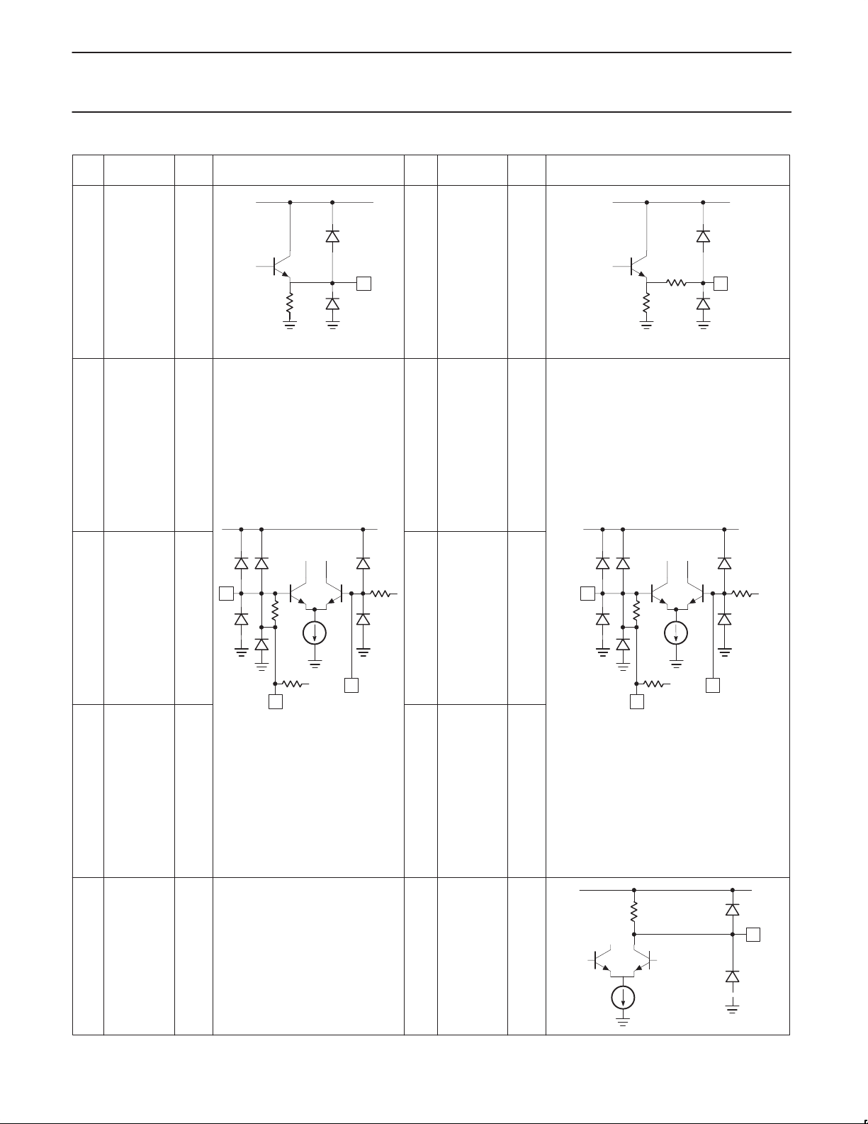
PIN
No.
PIN
MNEMONIC
DC V EQUIVALENT CIRCUIT
1 RF IN +2.35
2
3
RF
BYPASS
OSC
E
+1.56
+2.21
RF BYPASS
4
RF IN
1
18k
PIN
No.
400
30K
26
2
6V
7
MIX
PIN
MNEMONIC
CC
RSSI
OUT
DC V EQUIVALENT CIRCUIT
V
6
REF
+3.00
BANDGAP
+0.20
+
—
V
CC
7
V
4
5
OSC
B
OSC
BUFFER
+2.78
+2.21
3
150µA
RSSI
8
FEEDBACK
POWER
9
5
150µA
DOWN
+0.20
+2.00
9
CC
—
8
+
R
R
SR01729
1998 Aug 10
Figure 6.
10
Page 11
Philips Semiconductors Product specification
SA647Low-voltage digital IF receiver
PIN
No.
10
11
12
PIN
MNEMONIC
LIMITER
OUT
LIMITER
DC V EQUIVALENT CIRCUIT
PIN
No.
+1.25 16
11
8.8k
+1.28 17
PIN
MNEMONIC
IF
AMP OUT
IF AMP
DECOUPDECOUP
DC V EQUIVALENT CIRCUIT
+1.28
1.31k
6.6k
+1.28
16
14
+1.28 18
1.5k
50µA
12
13
+1.28 19
13
14
LIMITER
LIMITER
15 GND 0 20
IF
AMP INCOUPLING
IF AMP
DECOUPIN
MIXER
OUT
+1.28
+1.28
+2.03
18
1.5k
50µA
17
19
1.87k
20
1998 Aug 10
SR00509
Figure 7.
11
Page 12
Philips Semiconductors Product specification
SA647Low-voltage digital IF receiver
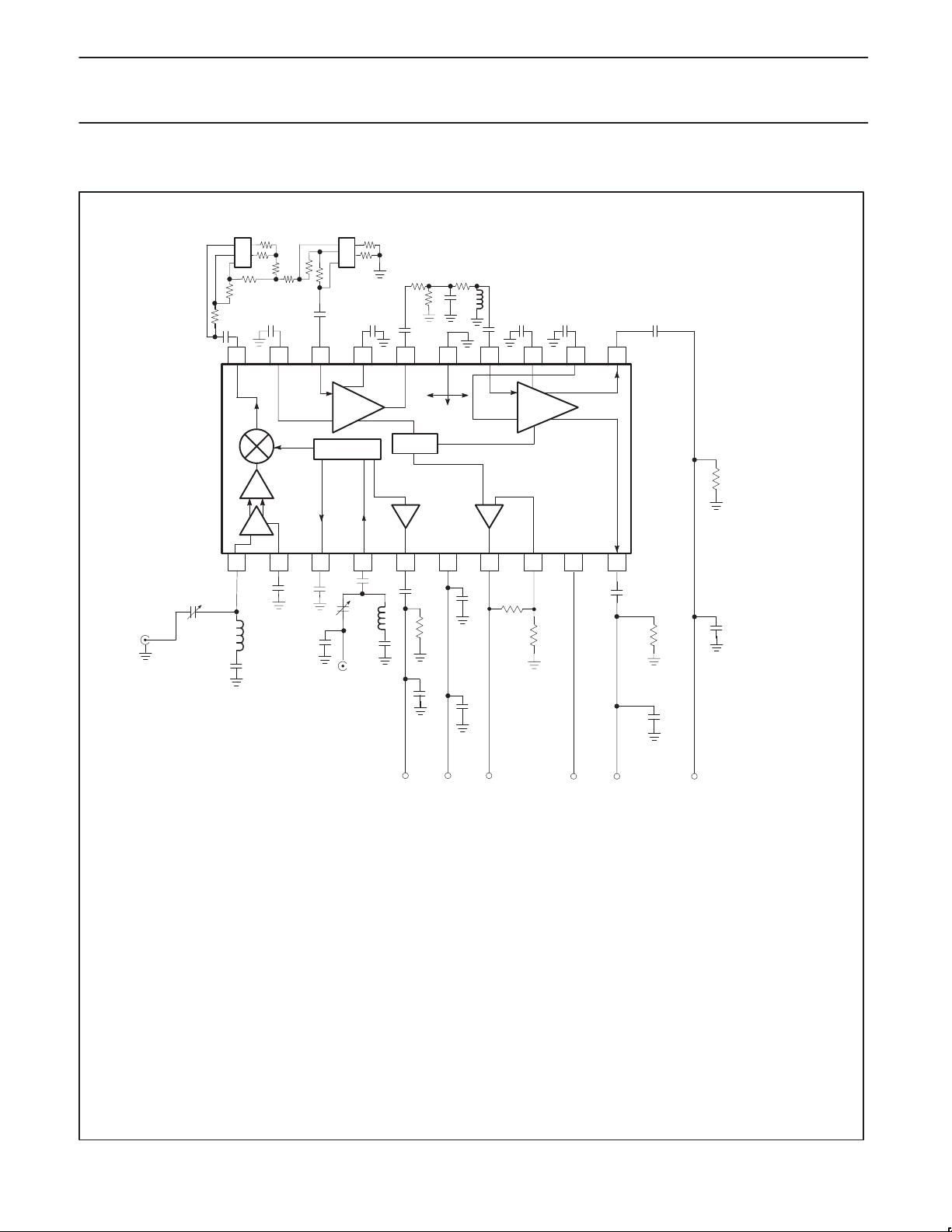
GENERAL APPLICATIONS CIRCUIT
FLT1 FLT2
R15
2
4
5
3
1
R16
R17
R18
R19
C25
20 19 18 17 16 14
C23
R14
R13
R11
R12
C24
R10
2
4
5
3
1
R9
C22
R7 R6
R8
C21
15
GND
C20
L3
C18 C17
C19
13 12 11
C16
RF
INPUT
+–
MIXER
IF
AMP
OSCILLATOR
RSSI
LO
BUFF
RSSI BUFF
LIMITER
R5
+–
RSSI FB
108764321 5 9
C5
LO
INPUT
C8
C9
C2
L2
C6
OSC
OUT
C11
R2
R1
C10
C12
RSSI
V
CC
R3
POWER
DOWN
LIMITER
OUT(–)
C13
R4
C14
LIMITER
OUT(+)
C15
C1
C4
L1
C3
C7
1998 Aug 10
Component List
C1 5–30pF C11 0.1mF C21 10nF R1 10KW R13 240W L1 180nH
C2 5–30pF C12 6.8pF C22 0.1mFR20W (short) R14 4.5KW L2 180nH
C3 0.1mF C13 0.1mF C23 0.1mF R3 OPEN R15 180W L3 56mH
C4 0.1mF C14 30pF C24 10nF R4 5.1k R16 180W FLT1,2 600kHz
C5 0.1mF C15 30pF C25 10nF R5 5.1k R17 240W
C6 0.1mF C16 0.1mFR60W (short) R18 10KW
C7 47pF C17 0.1mF R7 1.5KW R19 10KW
C8 1nF C18 0.1mF R8 1.5KW
C9 10pF C19 10nF R9 180W
C10 3.9pF C20 1500pF R10 180W
R11 10KW
R12 0KW
NOTE:
R2 and R3 set the RSSI buffer gain. For unity gain short R2 (Pin 7 to Pin 8)
and leave R9 open.
SR01730
Figure 8.
12
Page 13
Philips Semiconductors Product specification
SA647Low-voltage digital IF receiver
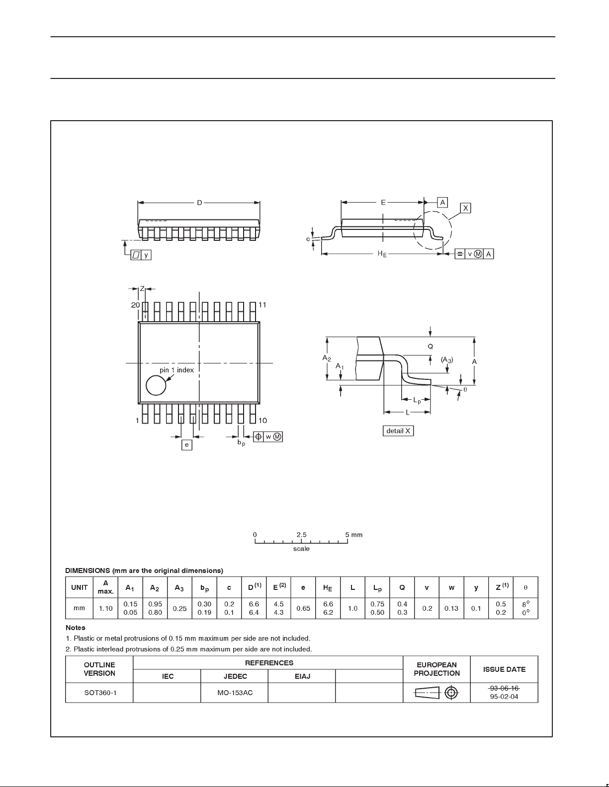
TSSOP20: plastic thin shrink small outline package; 20 leads; body width 4.4 mm SOT360-1
1998 Aug 10
13
Page 14

Philips Semiconductors Product specification
SA647Low-voltage digital IF receiver
Data sheet status
Data sheet
status
Objective
specification
Preliminary
specification
Product
specification
Product
status
Development
Qualification
Production
Definition
This data sheet contains the design target or goal specifications for product development.
Specification may change in any manner without notice.
This data sheet contains preliminary data, and supplementary data will be published at a later date.
Philips Semiconductors reserves the right to make chages at any time without notice in order to
improve design and supply the best possible product.
This data sheet contains final specifications. Philips Semiconductors reserves the right to make
changes at any time without notice in order to improve design and supply the best possible product.
[1]
[1] Please consult the most recently issued datasheet before initiating or completing a design.
Definitions
Short-form specification — The data in a short-form specification is extracted from a full data sheet with the same type number and title. For
detailed information see the relevant data sheet or data handbook.
Limiting values definition — Limiting values given are in accordance with the Absolute Maximum Rating System (IEC 134). Stress above one
or more of the limiting values may cause permanent damage to the device. These are stress ratings only and operation of the device at these or
at any other conditions above those given in the Characteristics sections of the specification is not implied. Exposure to limiting values for extended
periods may affect device reliability.
Application information — Applications that are described herein for any of these products are for illustrative purposes only. Philips
Semiconductors make no representation or warranty that such applications will be suitable for the specified use without further testing or
modification.
Disclaimers
Life support — These products are not designed for use in life support appliances, devices or systems where malfunction of these products can
reasonably be expected to result in personal injury . Philips Semiconductors customers using or selling these products for use in such applications
do so at their own risk and agree to fully indemnify Philips Semiconductors for any damages resulting from such application.
Right to make changes — Philips Semiconductors reserves the right to make changes, without notice, in the products, including circuits, standard
cells, and/or software, described or contained herein in order to improve design and/or performance. Philips Semiconductors assumes no
responsibility or liability for the use of any of these products, conveys no license or title under any patent, copyright, or mask work right to these
products, and makes no representations or warranties that these products are free from patent, copyright, or mask work right infringement, unless
otherwise specified.
Philips Semiconductors
811 East Arques Avenue
P.O. Box 3409
Sunnyvale, California 94088–3409
Telephone 800-234-7381
Copyright Philips Electronics North America Corporation 1998
All rights reserved. Printed in U.S.A.
Date of release: 08-98
Document order number: 9397 750 04241
1998 Aug 10
14
 Loading...