

Page 1
RF COMMUNICATIONS PRODUCTS
INPUT/OUTPUT
OUTPUT/INPUT
OUTPUT/INPUT
ENCH1
SA630
Single pole double throw (SPDT) switch
Product Specification
Replaces data of October 10, 1991
IC17 Data Handbook
1997 Nov 07
Philips Semiconductors
Page 2
Philips Semiconductors Product specification
SA630Single pole double throw (SPDT) switch
DESCRIPTION
The SA630 is a wideband RF switch fabricated in BiCMOS technology and incorporating on-chip CMOS/TTL compatible drivers. Its
primary function is to switch signals in the frequency range DC 1GHz from one 50Ω channel to another. The switch is activated by
a CMOS/TTL compatible signal applied to the enable channel 1 pin
(ENCH1).
The extremely low current consumption makes the SA630 ideal for
portable applications. The excellent isolation and low loss makes
this a suitable replacement for PIN diodes.
The SA630 is available in an 8-pin dual in-line plastic package and
an 8-pin SO (surface mounted miniature) package.
FEA TURES
•Wideband (DC - 1GHz)
•Low through loss (1dB typical at 200MHz)
•Unused input is terminated internally in 50Ω
•Excellent overload capability (1dB gain compression point +18dBm
at 300MHz)
•Low DC power (170µA from 5V supply)
•Fast switching (20ns typical)
•Good isolation (off channel isolation 60dB at 100MHz)
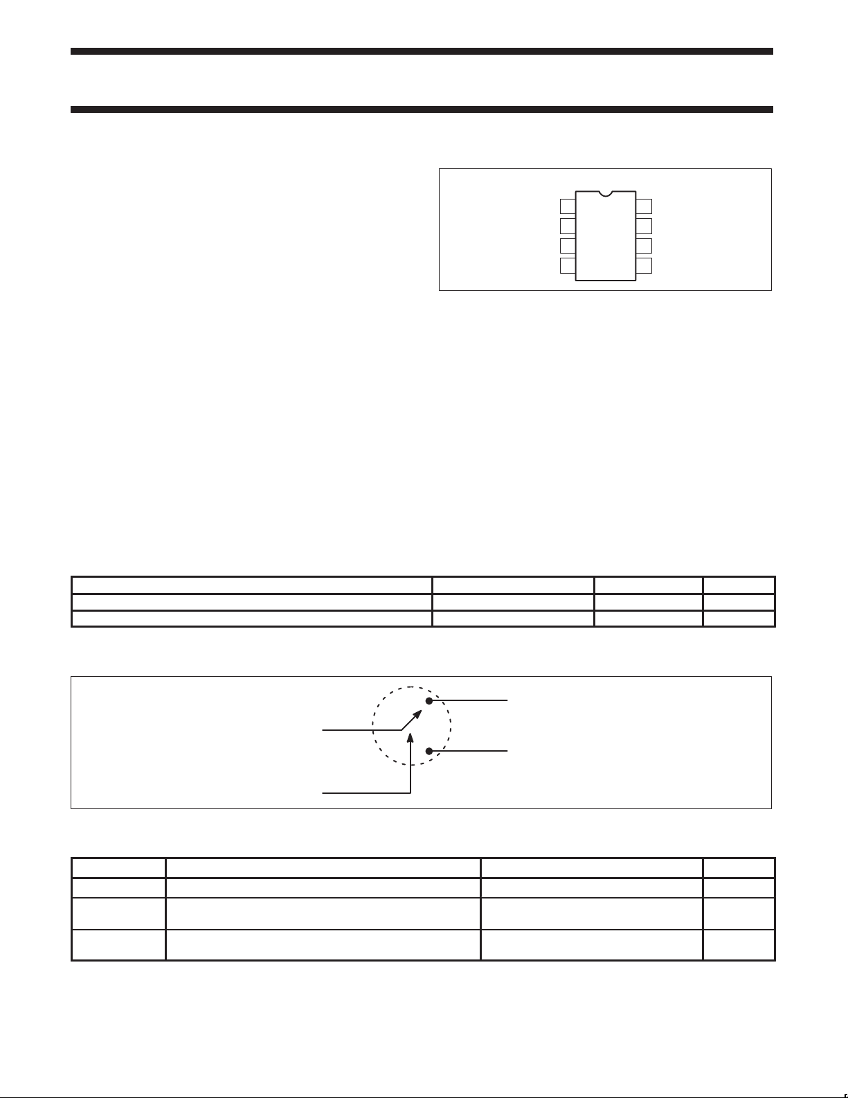
PIN CONFIGURATION
D and N Packages
•Low distortion (IP
1
V
DD
2
GND
3
INPUT
45
ENCH1
Figure 1. Pin Configuration
intercept +33dBm)
3
8
OUT
7
AC GND
6
GND
OUT
•Good 50Ω match (return loss 18dB at 400MHz)
•Full ESD protection
•Bidirectional operation
APPLICA TIONS
•Digital transceiver front-end switch
•Antenna switch
•Filter selection
•Video switch
•FSK transmitter
1
2
SR00578
ORDERING INFORMATION
DESCRIPTION TEMPERATURE RANGE ORDER CODE DWG #
8-Pin Plastic Dual In-Line Package (DIP) -40 to +85°C SA630N SOT97-1
8-Pin Plastic Small Outline (SO) package (Surface-mount) -40 to +85°C SA630D SOT96-1
BLOCK DIAGRAM
OUTPUT/INPUT
INPUT/OUTPUT
OUTPUT/INPUT
ENCH1
SR00579
Figure 2. Block Diagram
RECOMMENDED OPERATING CONDITIONS
SYMBOL PARAMETER RATING UNITS
V
DD
T
A
T
J
Supply voltage 3.0 to 5.5V V
Operating ambient temperature range
SA Grade
Operating junction temperature range
SA Grade
-40 to +85 °C
-40 to +105 °C
1997 Nov 07 853-1577 18666
2
Page 3
Philips Semiconductors Product specification
SA630Single pole double throw (SPDT) switch
EQUIVALENT CIRCUIT
V
DD
+5V
1
20kΩ
CONTROL
LOGIC
2
50Ω
8
7
OUT
1
AC BYPASS
INPUT
ENCH1
50Ω
3
4
20kΩ
6
OUT
5
2
SR00580
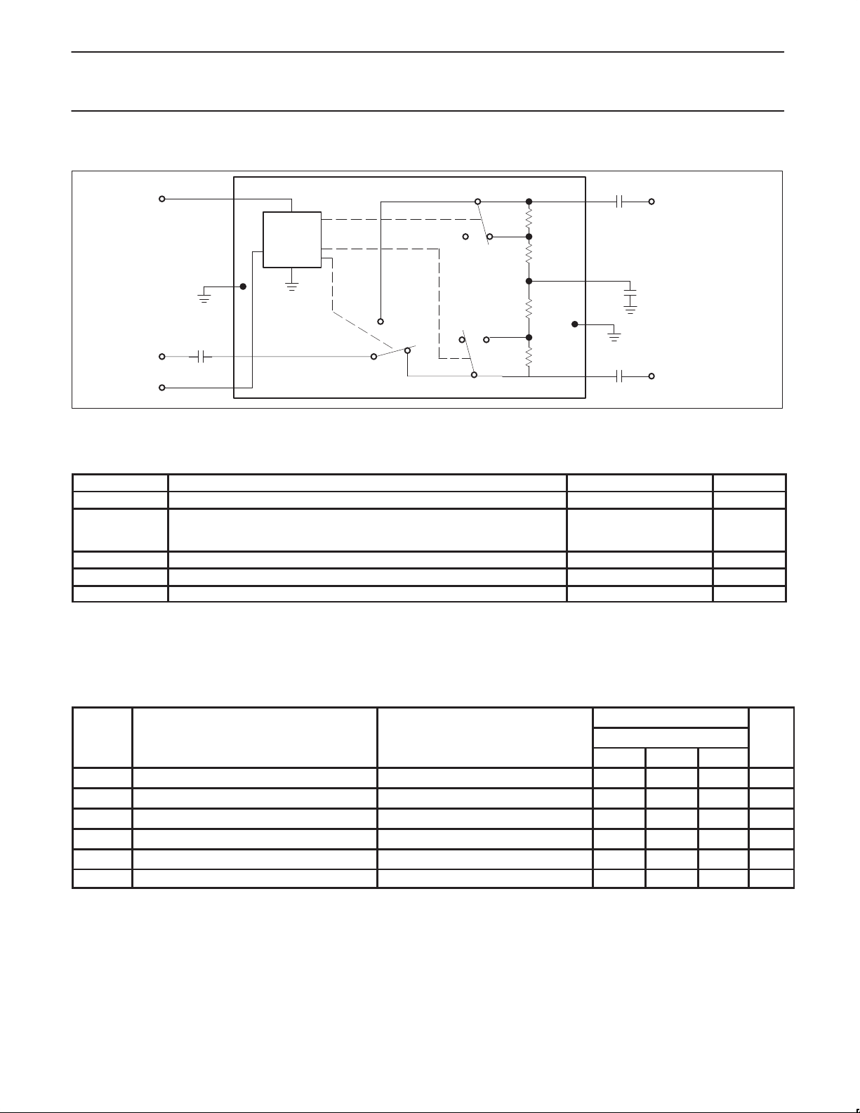
Figure 3. Equivalent Circuit
ABSOLUTE MAXIMUM RATINGS
SYMBOL PARAMETER RATING UNITS
V
T
P
T
DD
P
D
JMAX
MAX
STG
Supply voltage -0.5 to +5.5 V
Power dissipation, TA = 25oC (still air)
8-Pin Plastic DIP
8-Pin Plastic SO
1
1160
780
mW
mW
Maximum operating junction temperature 150 °C
Maximum power input/output +20 dBm
Storage temperature range -65 to +150 °C
NOTES:
1. Maximum dissipation is determined by the operating ambient temperature and the thermal resistance, θ
8-Pin DIP: θ
8-Pin SO: θ
= 108°C/W
JA
= 158°C/W
JA
:
JA
DC ELECTRICAL CHARACTERISTICS
VDD = +5V, TA = 25°C; unless otherwise stated.
LIMITS
SYMBOL PARAMETER TEST CONDITIONS SA630 UNITS
MIN TYP MAX
I
V
V
NOTE:
1. The ENCH1 input must be connected to a valid Logic Level for proper operation of the SA630.
Supply current 40 170 300 µA
DD
V
TTL/CMOS logic threshold voltage
T
Logic 1 level Enable channel 1 2.0 V
IH
Logic 0 level Enable channel 2 -0.3 0.8 V
IL
I
ENCH1 input current ENCH1 = 0.4V -1 0 1 µA
IL
I
ENCH1 input current ENCH1 = 2.4V -1 0 1 µA
IH
1
1.1 1.25 1.4 V
DD
V
1997 Nov 07
3
Page 4
Philips Semiconductors Product specification
SA630Single pole double throw (SPDT) switch
AC ELECTRICAL CHARACTERISTICS1 - D PACKAGE
VDD = +5V, TA = 25°C; unless otherwise stated.
LIMITS
SYMBOL PARAMETER TEST CONDITIONS SA630 UNITS
MIN TYP MAX
DC - 100MHz
S21, S12Insertion loss (ON channel)
S21, S12Isolation (OFF channel)
S11, S22Return loss (ON channel)
S11, S22Return loss (OFF channel)
t
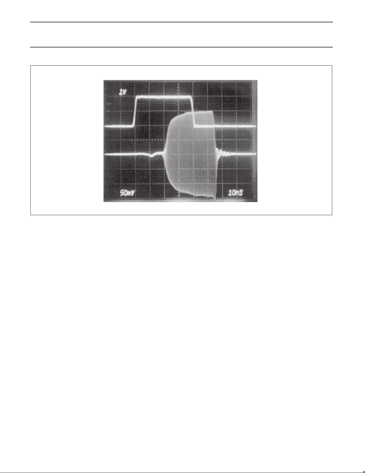
Switching speed (on-off delay) 50% TTL to 90/10% RF 20 ns
D
tr, t
P
IP
IP
NF Noise figure (ZO = 50Ω )
NOTE:
1. All measurements include the effects of the D package SA630 Evaluation Board (see Figure 4B). Measurement system impedance is 50Ω .
2. The placement of the AC bypass capacitor is critical to achieve these specifications. See the applications section for more details.
Switching speeds (on-off rise/fall time) 90%/10% to 10%/90% RF 5 ns
f
Switching transients 165 mV
1dB gain compression DC - 1GHz +18 dBm
-1dB
Third-order intermodulation intercept 100MHz +33 dBm
3
Second-order intermodulation intercept 100MHz +52 dBm
2
2
500MHz
900MHz
10MHz
100MHz
500MHz
900MHz
DC - 400MHz
900MHz
DC - 400MHz
900MHz
100MHz
900MHz
70
24
1
1.4
2
80
60
50
30
20
12
17
13
1.0
2.0
2.8
dB
dB
dB
dB
P-P
dB
AC ELECTRICAL CHARACTERISTICS1 - N PACKAGE
VDD = +5V, TA = 25°C; all other characteristics similar to the D-Package, unless otherwise stated.
LIMITS
SYMBOL PARAMETER TEST CONDITIONS SA630 UNITS
MIN TYP MAX
DC - 100MHz
S21, S12Insertion loss (ON channel)
S21, S12Isolation (OFF channel)
NF Noise figure (ZO = 50Ω )
NOTE:
1. All measurements include the effects of the N package SA630 Evaluation Board (see Figure 4C). Measurement system impedance is 50Ω .
APPLICATIONS
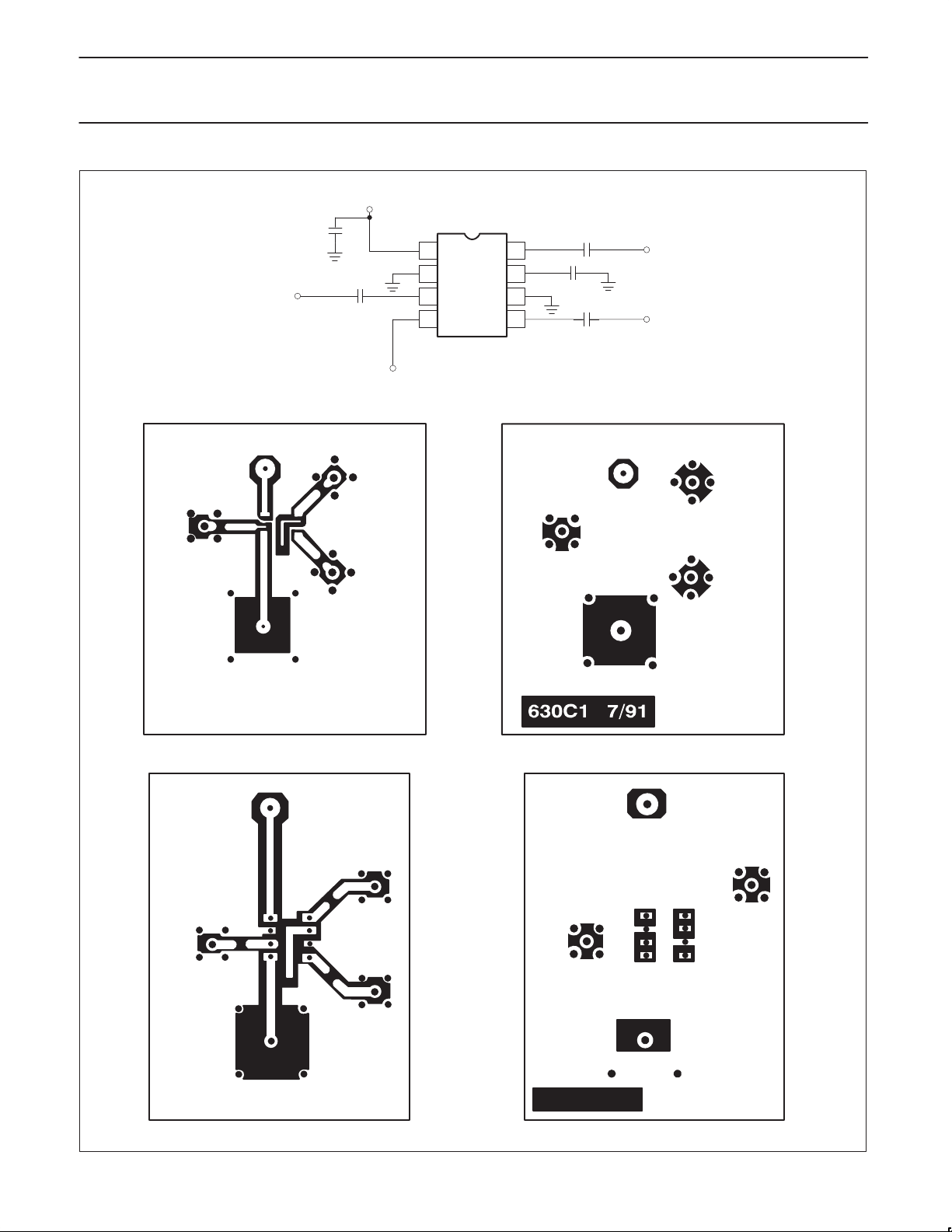
The typical applications schematic and printed circuit board layout of
the SA630 evaluation board is shown in Figure 4. The layout of the
board is simple, but a few cautions need to be observed. The input
and output traces should be 50Ω. The placement of the AC bypass
capacitor is
two channels is desired. The trace from Pin 7 should be drawn back
towards the package and then be routed downwards. The capacitor
extremely critical
if a symmetric isolation between the
500MHz
900MHz
10MHz
100MHz
500MHz
900MHz
100MHz
900MHz
should be placed straight down as close to the device as practical.
For better isolation between the two channels at higher frequencies,
it is also advisable to run the two output/input traces at an angle.
This also minimizes any inductive coupling between the two traces.
The power supply bypass capacitor should be placed close to the
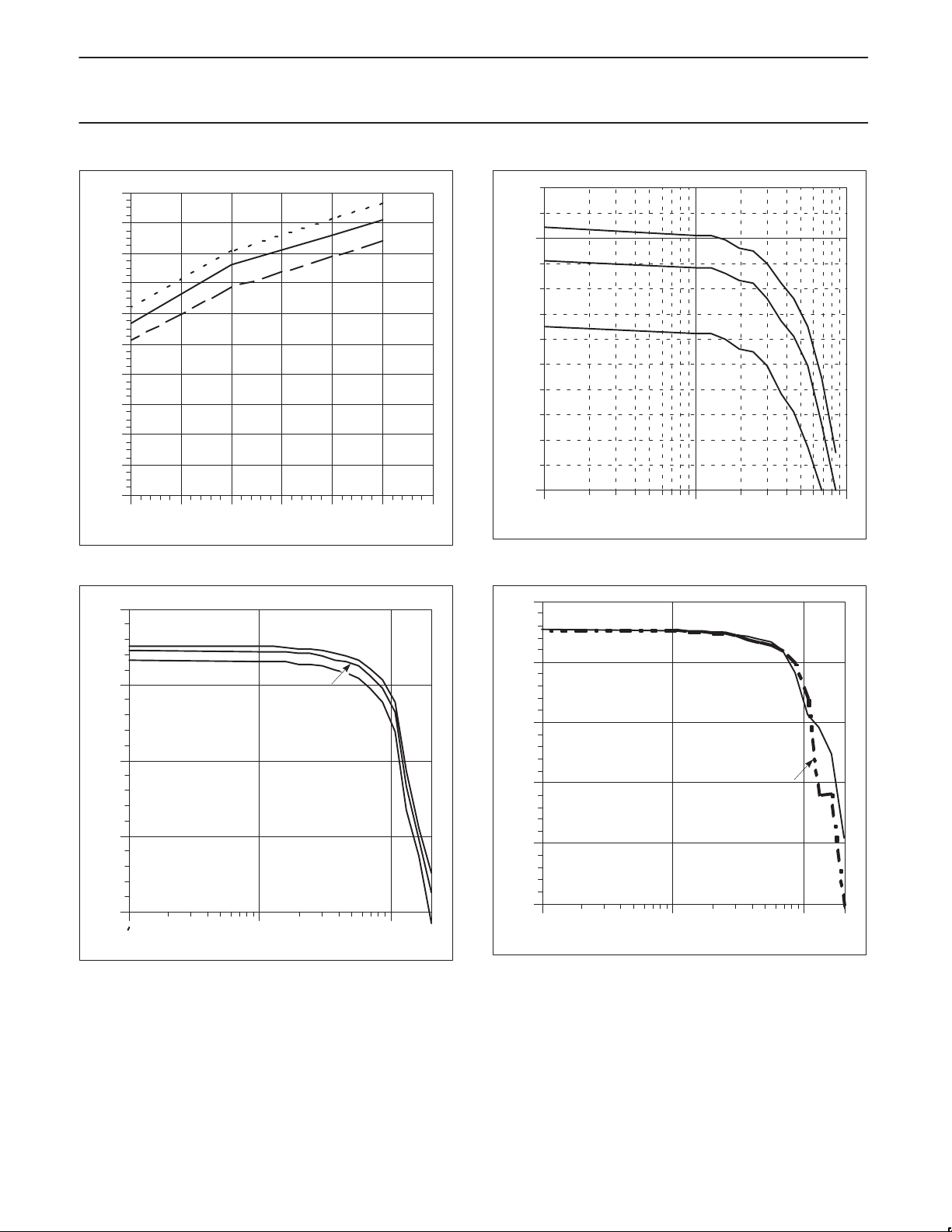
device. Figure 10 shows the frequency response of the SA630.
The loss matching between the two channels is excellent to 1.2GHz
as shown in Figure 13.
58
1
1.4
2.5
68
50
37
15
1.0
2.5
dB
dB
dB
1997 Nov 07
4
Page 5
Philips Semiconductors Product specification
SA630Single pole double throw (SPDT) switch
V
DD
+5V
0.1µF
INPUT
0.01µF
a. Evaluation Board Schematic
D and N Packages
1
GND
2
3
45
ENCH
1
8
7
6
AC GND
GND
0.01µF
0.01µF
0.01µF
OUT
OUT
1
2
1997 Nov 07
b. 630 D-Package Board Layout
630N1 7/91
c. 630 N-Package Board Layout
Figure 4. Board and Package Graphics
5
SR00581
Page 6

Philips Semiconductors Product specification
SA630Single pole double throw (SPDT) switch
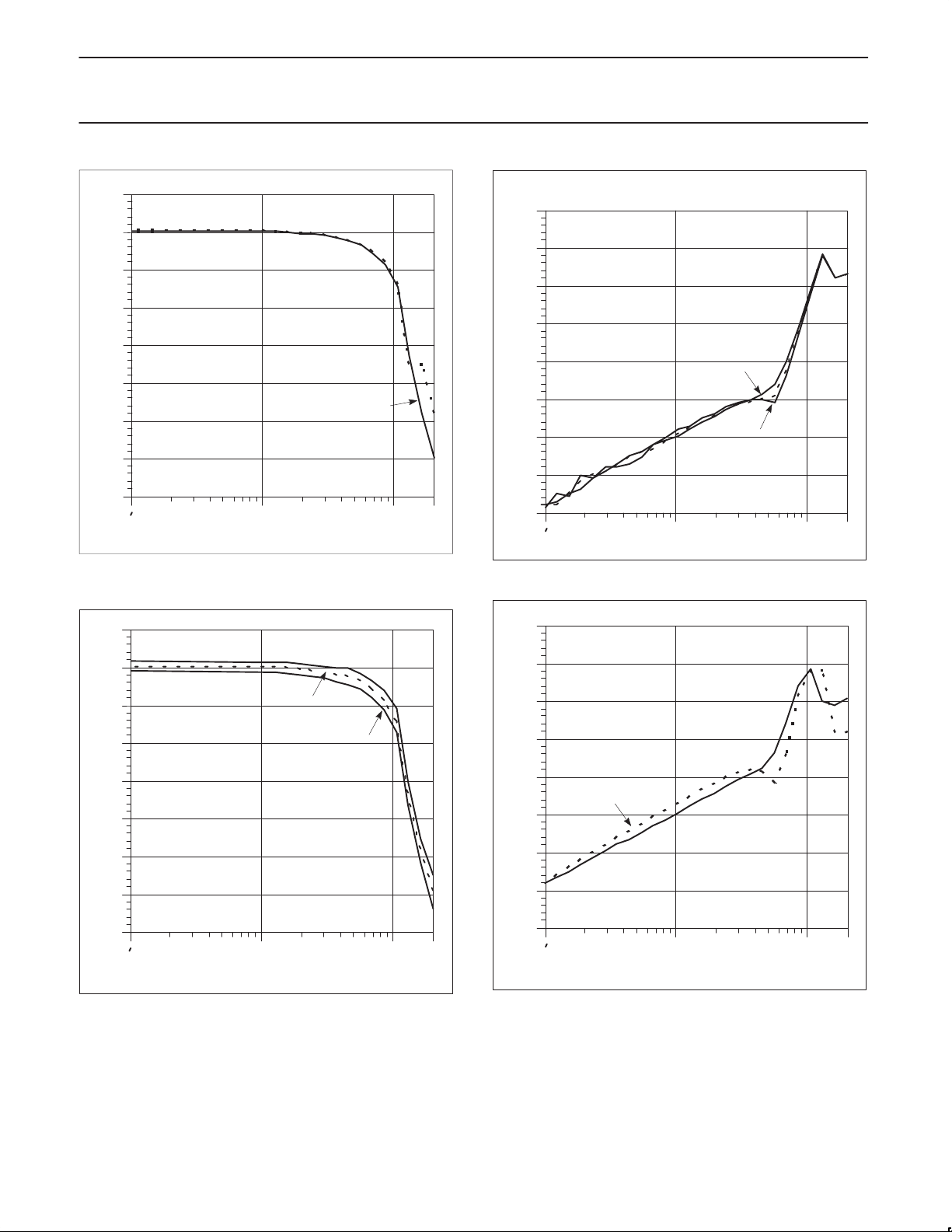
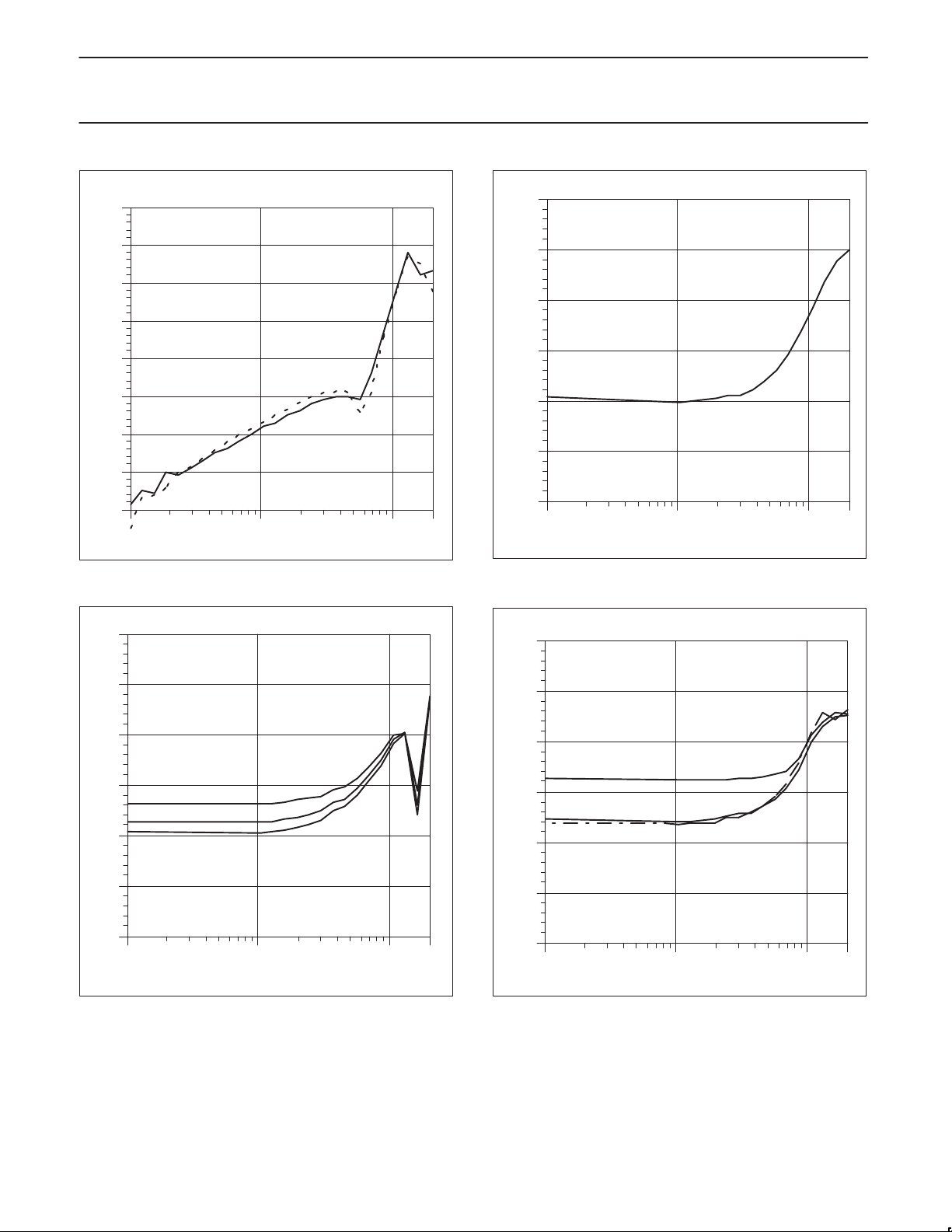
The isolation and matching of the two channels over frequency is
shown in Figures 15 and 17, respectively.
The SA630 is a very versatile part and can be used in many
applications. Figure 5 shows a block diagram of a typical Digital RF
transceiver front-end. In this application the SA630 replaces the
duplexer which is typically very bulky and lossy. Due to the low
power consumption of the device, it is ideally suited for handheld
applications such as in CT2 cordless telephones. The SA630 can
also be used to generate Amplitude Shift Keying (ASK) or On-Off
Keying (OOK) and Frequency Shift Keying (FSK) signals for digital
RF communications systems. Block diagrams for these applications
are shown in Figures 6 and 7, respectively.
For applications that require a higher isolation at 1GHz than
obtained from a single SA630, several SA630s can be cascaded as
5200
630
Tx/Rx
5200 VCO
shown in Figure 8. The cascaded configuration will have a higher
loss but greater than 35dB of isolation at 1GHz and greater than
65dB @ 500MHz can be obtained from this configuration. By
modifying the enable control, an RF multiplexer/ de-multiplexer or
antenna selector can be constructed. The simplicity of SA630
coupled with its ease of use and high performance lends itself to
many innovative applications.
The SA630 switch terminates the OFF channel in 50Ω. The 50Ω
resistor is internal and is in series with the external AC bypass
capacitor. Matching to impedances other than 50Ω can be achieved
by adding a resistor in series with the AC bypass capacitor (e.g.,
25Ω additional to match to a 75Ω environment).
602A IF OUT
MICRO
CONTROLLER
MODULATION
KEYPAD
&
DISPLAY
Figure 5. A Typical TDMA/Digital RF Transceiver System Front-End
ASK OUTPUT
630
OSCILLATOR
ENABLE
TTL DATA
CH1
50Ω
SR00583
Figure 6. Amplitude Shift Keying (ASK) Generator
f
1
FSK OUTPUT
630
ENABLE
CH1
f
2
TTL DATA
SR00584
Figure 7. Frequency Shift Keying (FSK) Gnerator
IN/OUT
630
ENABLE
SR00582
OUT1/IN1
630
630
OUT2/IN2
SR00585
Figure 8.
1997 Nov 07
6
Page 7
Philips Semiconductors Product specification
SA630Single pole double throw (SPDT) switch
200
180
160
140
µ
120
100
80
SUPPLY CURRENT ( A)
60
40
20
0
3 3.5 4 4.5 5 5.5 6
SUPPLY VOLTAGE (V)
Figure 9. Supply Current vs. VDD and Temperature
0
5V
–2
4V
+85°C
+25°C
-40°C
SR00586
5V
–1
21
S (dB)
–2
10 100 1000
4V
3V
= +25°C
T
A
FREQUENCY (MHz)
Figure 11. Loss vs. Frequency and VDD for
D-Package-Expanded Detail-
0
–2
SR00588
3V
–4
21
S (dB)
–6
TA = +25°C
–8
10 100 1000 2000
FREQUENCY (MHz)
Figure 10. Loss vs. Frequency and VDD for D-Package
SR00587
–4
21
S (dB)
–6
–8
VDD = 5V
= +25°C
T
A
–10
10 100 1000 2000
FREQUENCY (MHz)
CH2
SR00589
Figure 12. Loss Matching vs. Frequency for N-Package (DIP)
1997 Nov 07
7
Page 8
Philips Semiconductors Product specification
SA630Single pole double throw (SPDT) switch
0
0
–1
–10
–2
–20
–3
–30
–4
21
S (dB)
–5
CH1
–6
–7
–8
10 100 1000 2000
FREQUENCY (MHz)
VDD =
T
= +25°C
5V
A
SR00590
Figure 13. Loss Matching vs. Frequency; CH1 vs. CH2 for
D-Pakage
–40
21
S (dB)
–50
–60
–70
–80
10 100 1000 2000
FREQUENCY (MHz)
3V
4V
5V
TA = +25°C
SR00592
Figure 15. Isolation vs. Frequency and VDD for D-Package
0
–1
–2
–3
–4
21
S (dB)
–5
–6
–7
–8
10 100 1000 2000
FREQUENCY (MHz)
+25°C
-40°C
+85°C
VDD = 5V
Figure 14. Loss vs. Frequency and Temperature for
D-Package
SR00591
0
–10
–20
–30
–40
21
S (dB)
–50
–60
–70
–80
10 100 1000 2000
CH2
TA = +25°C
V
DD
FREQUENCY (MHz)
= 5V
SR00593
Figure 16. Isolation Matching vs. Frequency for N-Package
(DIP)
1997 Nov 07
8
Page 9
Philips Semiconductors Product specification
SA630Single pole double throw (SPDT) switch
0
–10
–20
–30
–40
21
S (dB)
–50
–60
–70
–80
10 100 1000 2000
FREQUENCY (MHz)
CH2
CH1
VDD = +5V
TA = +25°C
SR00594
Figure 17. Isolation Matching vs. Frequency; CH1 vs. CH2 for
D-Package
0
0
–5
–10
22
–15
S (dB)
–20
–25
–30
10 100 1000 2000
FREQUENCY (MHz)
VDD = 5V
= +25°C
T
A
Figure 19. Output Match On-Channel vs. Frequency
0
SR00597
–5
–10
–15
11
S (dB)
–20
–25
–30
10 100 1000 2000
3V
4V
5V
TA = +25°C
FREQUENCY (MHz)
SR00595
Figure 18. Input Match On-Channel vs. Frequency and V
DD
–5
–10
CH1: 3V
22
–15
S (dB)
–20
–25
–30
CH1: 5V
CH2: 5V
T
= +25°C
A
10 100 1000 2000
FREQUENCY (MHz)
Figure 20. OFF-Channel Match vs. Frequency and V
SR00597
DD
1997 Nov 07
9
Page 10
Philips Semiconductors Product specification
SA630Single pole double throw (SPDT) switch
0
–5
–10
–15
22
S (dB)
–20
–25
–30
10 100 1000 2000
+85°C
+25°C
-40°C
VDD = 5V
FREQUENCY (MHz)
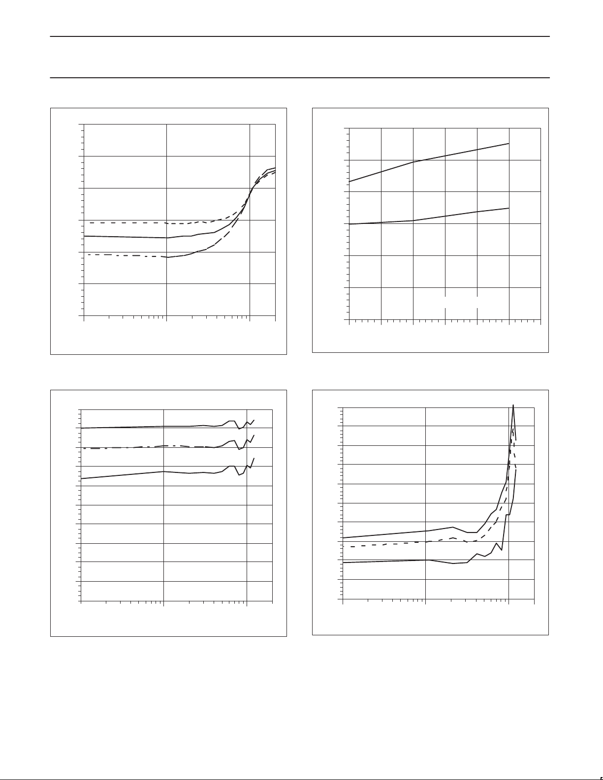
Figure 21. OFF Channel Match vs. Frequency and
Temperature
20
SR00598
60
50
IP2
40
30
20
INTERCEPT POINT (dBm)
10
0
3 3.5 4 4.5 5 5.5 6
5
IP3
TA = +25°C
SUPPLY VOLTAGE (V)
Figure 23. Intercept Points vs.V
DD
SR00633
18
16
14
12
10
-1
P (dBm)
8
6
4
2
0
10 100 1000 2000
5V
4V
3V
TA = +25°C
FREQUENCY (MHz)
Figure 22. P-1 dB vs. Frequency and V
DD
SR00599
4.5
3.5
2.5
NOISE FIGURE (dB)
1.5
0.5
T
= +25°C
A
4
Z
= 50Ω
O
3
2
3V
4V
1
5V
0
10 100 1000 2000
FREQUENCY (MHz)
SR00634
Figure 24. Noise Figure vs. Frequency and VDD for D-Package
1997 Nov 07
10
Page 11
Philips Semiconductors Product specification
SA630Single pole double throw (SPDT) switch
ENCH1 (Pin4)
OUT1 (Pin 8)
Figure 25. Switching Speed; fIN = 100MHz at -6dBm, VDD = 5V
SR00635
1997 Nov 07
11
Page 12
Philips Semiconductors Product specification
SA630Single pole double throw (SPDT) switch
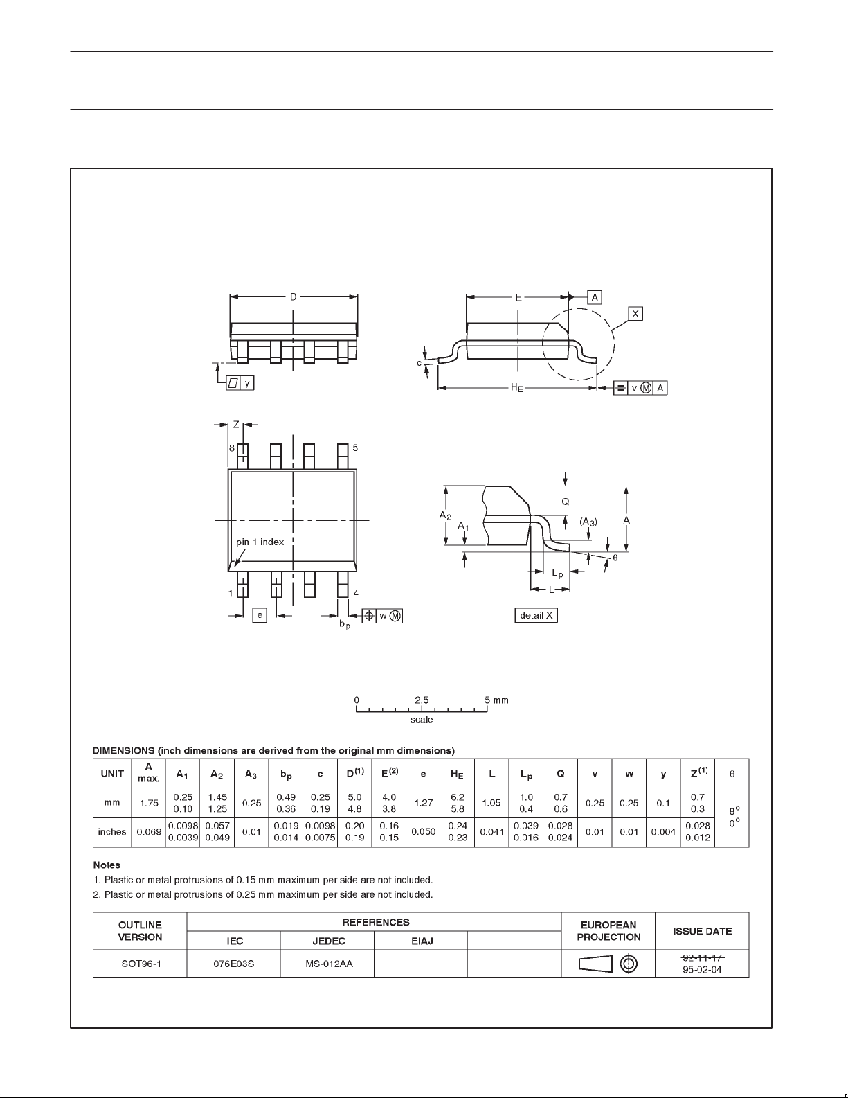
SO8: plastic small outline package; 8 leads; body width 3.9mm SOT96-1
1997 Nov 07
12
Page 13
Philips Semiconductors Product specification
SA630Single pole double throw (SPDT) switch
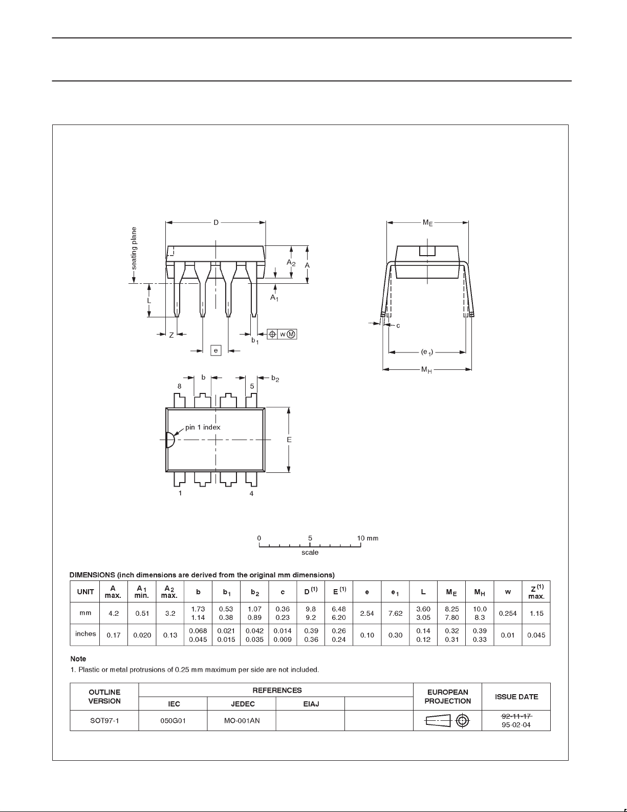
DIP8: plastic dual in-line package; 8 leads (300 mil) SOT97-1
1997 Nov 07
13
Page 14

Philips Semiconductors Product specification
SA630Single pole double throw (SPDT) switch
DEFINITIONS
Data Sheet Identification Product Status Definition
Objective Specification
Preliminary Specification
Product Specification
Formative or in Design
Preproduction Product
Full Production
Philips Semiconductors and Philips Electronics North America Corporation reserve the right to make changes, without notice, in the products,
including circuits, standard cells, and/or software, described or contained herein in order to improve design and/or performance. Philips
Semiconductors assumes no responsibility or liability for the use of any of these products, conveys no license or title under any patent, copyright,
or mask work right to these products, and makes no representations or warranties that these products are free from patent, copyright, or mask
work right infringement, unless otherwise specified. Applications that are described herein for any of these products are for illustrative purposes
only. Philips Semiconductors makes no representation or warranty that such applications will be suitable for the specified use without further testing
or modification.
LIFE SUPPORT APPLICA TIONS
Philips Semiconductors and Philips Electronics North America Corporation Products are not designed for use in life support appliances, devices,
or systems where malfunction of a Philips Semiconductors and Philips Electronics North America Corporation Product can reasonably be expected
to result in a personal injury. Philips Semiconductors and Philips Electronics North America Corporation customers using or selling Philips
Semiconductors and Philips Electronics North America Corporation Products for use in such applications do so at their own risk and agree to fully
indemnify Philips Semiconductors and Philips Electronics North America Corporation for any damages resulting from such improper use or sale.
Philips Semiconductors
811 East Arques Avenue
P.O. Box 3409
Sunnyvale, California 94088–3409
Telephone 800-234-7381
This data sheet contains the design target or goal specifications for product development. Specifications
may change in any manner without notice.
This data sheet contains preliminary data, and supplementary data will be published at a later date. Philips
Semiconductors reserves the right to make changes at any time without notice in order to improve design
and supply the best possible product.
This data sheet contains Final Specifications. Philips Semiconductors reserves the right to make changes
at any time without notice, in order to improve design and supply the best possible product.
Copyright Philips Electronics North America Corporation 1997
All rights reserved. Printed in U.S.A.
1997 Nov 07
14
 Loading...