

Page 1

INTEGRATED CIRCUITS
SA5753
Audio processor — filter and control
section
Product specification
Replaces data of 1995 July 7
IC17 Data Handbook
1997 Nov 07
Page 2
Philips Semiconductors Product specification
SA5753Audio processor – filter and control section
DESCRIPTION
The SA5753 is a high performance low power CMOS audio signal
processing system especially designed to meet the requirements for
small size and low voltage operation of hand-held equipment. The
SA5753 subsystem includes complementary transmit/receive voice
band (300-3000Hz), switched capacitor bandpass filters with
pre-emphasis and de-emphasis respectively, a transmit low pass
filter, peak deviation limiter for transmit, digitally controlled
attenuators for signal level and volume control, audio path mute
switches, a programmable DTMF generator, power-down circuitry
for low current standby, power-on reset capability, and an I
2
C
interface. When the SA5753 is used with an SA5752 (companding
function), the complete audio processing system of an AMPS,
TACS, NAMPS or NTACS cellular telephone is easily implemented.
The system also meets the requirements of the proposed NAMPS or
NTACS specification, and can be used in cordless telephone
applications.
The SA5753 can be operated without the I
2
C bus interface by
pulling DFT (Pin 13) HIGH.
BENEFITS
•Very compact application
•Long battery life in portable equipment
•Complete cellular audio function with the SA5752
APPLICATIONS
•Cellular radio
•Mobile communications
•High performance cordless telephones
•2-way radio
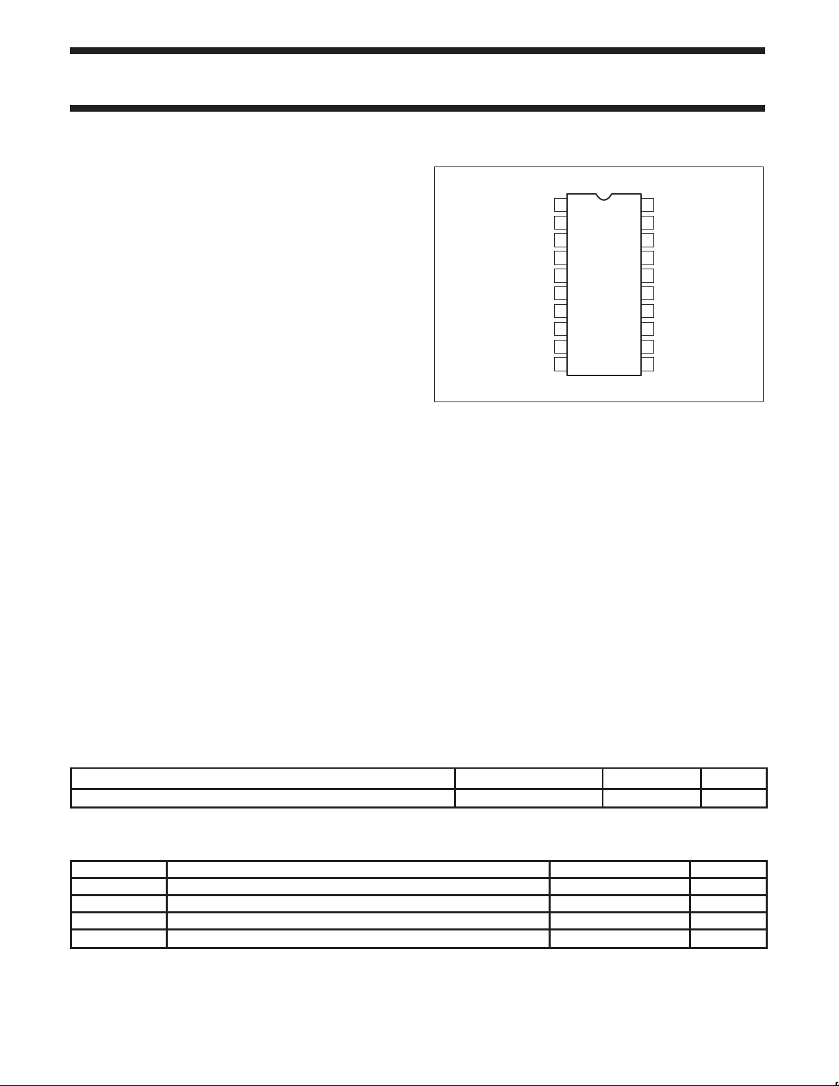
PIN CONFIGURATION
DK Package
TXBF
TXBF
PREMP
VOX
DEMP
AUDIO
SPKR
EAR
OUT
V
DD
CTL
HPDN
OUT
OUT
OUT
1
IN
2
3
IN
4
5
6
SA5753
7
8
IN
9
10
20
19
18
17
16
15
14
13
12
11
TX
OUT
DATA
IN
TX MUTE
SDA
SCL
GND
CLK
IN
DFT
RX MUTE
RX DEMOD
IN
SR00666
Figure 1. Pin Configuration
FEATURES
•Low 3V supply
•Miniature SSOP package
•Low power
•High performance
•Built-in programmable DTMF generator
•Built-in digitally controlled attenuators for modulation and volume
control
•Built-in peak-deviation limiter
2
•I
C Bus controlled
•Power-on reset
•Power down capability
•Programmable mute control
•Meets AMPS/TACS/NAMPS/NTACS requirements
ORDERING INFORMATION
DESCRIPTION TEMPERATURE RANGE ORDER CODE DWG #
20-Pin Plastic Shrink Small Outline Package (SSOP) -40 to +85°C SA5753DK SOT266-1
ABSOLUTE MAXIMUM RATINGS
SYMBOL PARAMETER RATING UNIT
V
DD
V
IN
T
A
1997 Nov 07 853-1722 18666
Power supply voltage range -0.3 to 6 V
Voltage applied to any other pin -0.3 to VDD+0.3 V
Storage temperature -65 to +150
Ambient operating temperature -40 to +85
2
o
°C
C
Page 3

Philips Semiconductors Product specification
SA5753Audio processor – filter and control section
PIN DESCRIPTIONS
PIN NO. SYMBOL DESCRIPTION
1 TXBF
2 TXBF
3 PREMP
4 V
5 VOX
IN
OUT
IN
DD
CTL
6 HPDN Power-down I/O
7 DEMP
8 AUDIO
9 SPKR
10 EAR
11 RX DEMOD
OUT
IN
OUT
OUT
IN
12 RX MUTE RX audio signal mute input
13 DFT Default input, non-I2C or stand-alone operation
14 CLK
IN
15 GND Ground
16 SCL I2C serial clock line
17 SDA I2C serial data line
18 TX MUTE Tx audio signal mute input
19 DATA
20 TX
IN
OUT
Transmit bandpass filter input
Transmit bandpass filter output
Pre-emphasis input
Positive supply
Vox control output
De-emphasis output
Audio input
Audio output to speaker
Audio output to earpiece
Rx demodulated audio signal input
Clock input (1.2MHz)
Data input
Transmit output
1997 Nov 07
3
Page 4
Philips Semiconductors Product specification
SYMBOL
PARAMETER
TEST CONDITIONS
UNIT
SYMBOL
PARAMETER
TEST CONDITIONS
UNIT
SA5753Audio processor – filter and control section
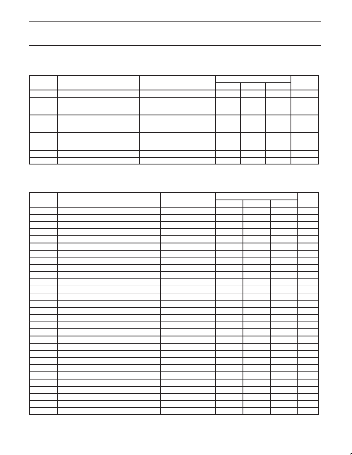
DC ELECTRICAL CHARACTERISTICS
TA = 25oC, VDD = +3.3V , unless otherwise specified. See test circuit, Figure 2.
LIMITS
MIN TYP MAX
V
DD
I
DD
I
IH
I
IL
V
V
AC ELECTRICAL CHARACTERISTICS
TA = 25oC, VDD = +3.3V. See test circuit, Figure 2. Clock frequency = 1.2MHz; test level = 0dBV = 77.5mV
specified. All gain control blocks (Attenuators) = 0dB gain, NAMPS and VCO bits set to 0.
Power supply voltage 3.0 3.3 5.5 V
Operating
Supply current
IDLE
Power Down (PWDN)
Input current high
TX MUTE, RX MUTE, HPDN
DFT
Input current low
TX MUTE, RX MUTE,
HPDN, DFT
Input voltage high 0.7V
IH
Input voltage low 0 0.3V
IL
VIN = V
DD
VIN = GND
–10
0
–30
–10
DD
1.7
600
200
0
+10
+10
+30
–10
0
+10
V
= -20dBm, unless otherwise
RMS
LIMITS
MIN TYP MAX
RX BPF anti alias rejection 40 dB
RX BPF input impedance f= 1kHz 100 kΩ
RX BPF gain with de-emphasis f = 1kHz -1.0 0 1.0 dB
RX BPF gain with de-emphasis f = 100Hz -30 dBm0
RX BPF gain with de-emphasis f = 300Hz 8.5 9.6 11.5 dBm0
RX BPF gain with de-emphasis f = 3kHz -11.5 -10.0 -8.5 dBm0
RX BPF gain with de-emphasis f = 5.9kHz -58 dBm0
RX BPF noise with de-emphasis 300Hz-3kHz 200 µV
RX dynamic range with deemphasis 80 dB
DEMP
DEMP
SPKR
EAR
SPKR
output impedance f = 1kHz 40 Ω
OUT
output swing (1%) 2kΩ to V
OUT
ouput swing (1%) 50kΩ toV
OUT
output swing (1%) 50kΩ to V
OUT
noise / EAR
OUT
noise 200 µV
OUT
; f = 1kHz 2.4 V
DD/2
; f = 1kHz VDD -1 2.4 V
DD/2
f = 1kHz VDD -1 2.4 V
DD/2;
CLKIN high 2.1 3.0 V
CLKIN low 0 1.0 V
TX BPF anti alias rejection f > 50kHz 40 dB
TX BPF input impedance f = 3kHz 100 KΩ
TX BPF noise 300 - 3000kHz 200 µV
TX LPF gain f = 5.9kHz -39 -36 dBm0
TX LPF gain with pre-emphasis f = 1kHz, 0dBV 2.43 dB
TX LPF gain with pre-emphasis f = 100Hz -19 dBm0
TX LPF gain with pre-emphasis f = 300Hz -10.45 dBm0
TX LPF gain with pre-emphasis f = 3kHz 9.14 dBm0
TX LPF gain with pre-emphasis f = 5900Hz -28 dBm0
TX LPF gain with pre-emphasis f = 9kHz -48 dBm0
TX overall gain 1kHz 2.43 dB
TX overall gain 100Hz -58 -44 dBm0
TX overall gain 300Hz -11.5 -10.4 -8.5 dBm0
0
DD
DD
mA
µA
µA
µA
µA
µA
µA
V
V
RMS
P-P
P-P
P-P
RMS
RMS
1997 Nov 07
4
Page 5
Philips Semiconductors Product specification
SYMBOL
PARAMETER
TEST CONDITIONS
UNIT
SYMBOL
Bits
TYPICAL STEP (dB)
SA5753Audio processor – filter and control section
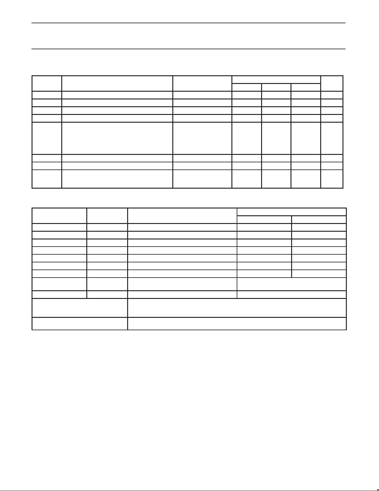
AC ELECTRICAL CHARACTERISTICS (continued)
LIMITS
MIN TYP MAX
TX overall gain 3kHz 8 9 9.6 dBm0
TX overall gain 5.9kHz -52 -45 dBm0
TX BPF dynamic range TBD dB
PREMP
TX
Tx DTMF signal with TXLPF and pre-emphasis 0.45 V/kHz
Rx DTMF sidetone –0.8 5.2 dBm0
input impedance f = 3kHz 100 kΩ
IN
Slew rate CL = 15pF 0.75 V/µs
OUT
Output impedance f = 3kHz 40 Ω
Output swing (limiting) 1.2 V
Output swing (1% THD)
5kΩ load (25°C)
1.0 V
P-P
P-P
Time delay to mute from RX MUTE or TX MUTE
transition
VIN = VIL to V
VIN = VIH to V
Table 1. Gain Control Blocks (Bit 0 is Least Significant Bit)
A1 4 –0.8 –12.0 0
A2a 5 ±0.25 –3.75 +3.75
A2b 2 –6, (–12 on first) –24.0 0
A3 4 –1.0 –17.0 –2.0
A4 4 ±0.5 –3.5 +3.5
A6 4 –2.0 –30.0 0
A7 4 ±0.5 –3.5 +3.5
NAMPS 1
VCO 1 +6.0 in A4
MSB sets the sign of the gain
For A2a, A4 and A7:
MSB = 0 for gain
MSB = 1 for attenuation
For all Gain Blocks:
FUNCTIONAL DESCRIPTION
All bits set to 0 = 0dB gain
All bits set to 1 = maximum gain or attenuation
a. A1 compensates for microphone gain variations in the transmit
The SA5753 is an audio signal processor designed to meet the
requirements of compact low voltage radio telephone equipment. It
includes transmit and receive bandpass filters for voiceband
b. A2a compensates for transmitter dynamic range variations due to
(300-3000Hz) with pre-emphasis and de-emphasis respectively, a
transmit peak deviation limiter , voice channel mute switches and a
data path which can be summed into the transmit channel. An I
2
C
interface is provided for software programmability of a DTMF
generator, mute polarity, selection of different power down and
operating modes and control of the gain in both the transmit and
c. A2b allows coarse attenuation to be inserted in the transmit path
receive channels.
Software programmable gain control allows the device to be
automatically optimized during equipment production and offers
d. A3 sets the gain between the DA TA
flexibility during normal operation.
Gain Blocks
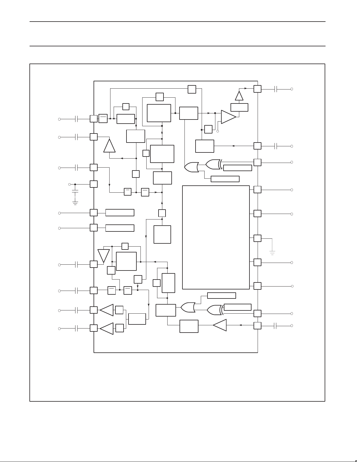
The programmable gain blocks are shown in Table 1 and Figure 2.
The purpose for each block is as follows:
IH
IL
0.5
0.5
µs
µs
TYPICAL GAIN (dB)
MIN MAX
+1.9 in A2b
–7.6 in A4
path.
manufacturing tolerances of the SA5753 and SA5752 compandor
companion device. To meet AMPS requirements, the dynamic
range between the zero crossing signal level of the compandor
and the peak signal allowed by the deviation limiter is adjusted to
12.34dB.
to eliminate positive feedback effects in hands-free speaker
applications. First step is 12dB followed by two steps of 6dB.
pin (Pin 19) and the TX
IN
OUT
pin (Pin 20) and should be adjusted after A2a and A4 have been
previously optimized. The SA5753 will interface directly with the
UMA1000T data processor (which produces a 2Vpk data signal).
For NAMPS applications an additional 10 to 14dB resistive divider
must be added at the DATA
pin (Pin 19) for a 2V data signal.
IN
1997 Nov 07
5
Page 6

Philips Semiconductors Product specification
SA5753Audio processor – filter and control section
e. A4 compensates for transmit gain variations due to manufacturing
tolerances of the SA5753, SA5752 and VCO connected to TX
OUT
(Pin 20). After A2a has been adjusted to set dynamic range then
A4 is used to set the peak output voltage at TX
(Pin 20) such
OUT
that a nominal 10kHz/V VCO produces a peak deviation of 12kHz
to meet AMPS specifications.
f. A6 is the volume control for both the SPKR
OUT
and EAR
OUT
.
g. A7 compensates for manufacturing tolerances in the SA5753 and
preceeding demodulator. For AMPS requirements, a 1kHz tone
with 2.9kHz deviation should produce an output signal at
DEMP
(Pin 7) corresponding to the zero crossing signal level
OUT
of the expandor.
NAMPS and VCO Offsets
For NAMPS applications, a ‘1’ programmed into R5B3 (register 5, bit
3) will offset the transmit gain for NAMPS applications. It is
recommended that A2a and A4 be programmed after the NAMPS
option is set to compensate for manufacturing tolerances in the
NAMPS offset, itself.
When the VCO bit of R5B2 is a ‘1’, an extra gain of 6dB is provided
at TX
for direct interface to VCOs with a nominal gain of 5kHz/V.
OUT
Operation Using the I2C Communications Bus
The SA5753 includes on-chip gain blocks and options which can be
programmed through an I
the DFT pin (Pin 13) must be pulled LOW. In this mode, all signal
level adjustments can be made through software with no external
potentiometers required.
With DFT pulled LOW, the HPDN pin (Pin 6) is an OUTPUT having
the same value as the program bit in register 5 bit 1 (R5B1) of the
control register bit map. The value at the VOX
the same as the program bit in R8B7. The HPDN and VOX
outputs can be used to control the state of the SA5752 companion
device.
2
C interface bus. To use this capability,
output (Pin 5) is
CTL
CTL
Power On Reset and Power Down Modes
In order to avoid undefined states of the SA5753 when power is
initially applied, a power-on-reset circuit is incorporated which
defaults RxP and TxP such that the receive and transmit paths are
muted if a ‘high’ voltage is applied to RX MUTE and TX MUTE (Pins
12 and 18). RX MUTE and TX MUTE include on-chip pull up
resistors so, during power up, the user may apply a logic ‘1’ to these
pins or leave them floating. After power up, the registers can be
programmed and the mutes removed by a quick access write to R0.
Three software controlled low power modes are provided on the
SA5753. These are POWER DOWN (PWDN), IDLE and DENA and
can be selected by programming a ‘1’ into R6B2, R6B1 or R6B0 as
follows. In PWDN mode (R6B2=1) both the voice and data
channels are powered down with the respective I/O pins at a high
impedance. In DENA mode (R6B1=1) the voice channels are
powered down, but the data channel (from DATA
fully active. In IDLE mode (R6B1=1, R6B0=1) both voice and data
channels are powered down. (See Table on page 8.)
The difference between selecting IDLE and PWDN is that the former
maintains the normal operational bias voltages at all voice and data
I/O pins and provides a glitch-free transfer from power down to a
fully active mode and vice-versa.
and TX
IN
OUT
) is
Although the POWER DOWN mode exhibits lower power
consumption, glitches may occur when transferring to an active
mode because of the previous high impedance of the I/O pins.
The VOX
and HPDN pins (Pins 5 and 6) still have the same
CTL
value as R8B7 and R5B1 in all low power modes.
Operation Without Using the I2C Bus
The SA5753 can be operated in a default mode with the I2C bus
bypassed. To use this mode, the DFT pin (Pin 13) is pulled HIGH,
then the I
register bits in the I
2
C bus is bypassed and the SA5753 operates as if all
2
C address map table are set to ‘0’ except R1B2
(S13), R0B0 (S10) and R0B1 (S9), which are set to ‘1’ to enable the
receiver output. R6B2 (PWDN), which is controlled by the state of
the HPDN pin (Pin 6), which is an input in DEFAULT mode.
When HPDN is pulled HIGH, the R6B2 bit is set to ‘0’ and the
SA5753 is placed in it’s normal operating mode with all Gain Control
Blocks set to 0dB except A3, which is set to –2dB.
When HPDN is pulled LOW, the R6B2 bit is set to ‘1’ and the
SA5753 enters POWER DOWN.
There is no on-chip pull-up or pull-down structure on the HPDN pin
and so it must not be allowed to float in DEFAULT mode since the
operating mode of the SA5753 will then be undetermined.
The Tx MUTE and Rx MUTE pins must be pulled LOW to enable the
transmit and receive paths, respectively.
The VOXCTL pin (Pin 5) will follow the value of the control bit stored
in R8B7 prior to pulling DFT HIGH.
The DTMF is disabled in the DEFAULT mode.
Programming Without the I2C Protocol
In the default mode, with DFT (Pin 13) and HPDN (Pin 6) pulled
HIGH, the registers in the control register bit map are chained
together so that bit 0 of a register is connected to bit 7 of the
preceeding register with R0B6, R0B7, R1B6 and R1B7 bypassed,
i.e., R0B5 is connected to R1B0, R1B5 is connected to R2B0, R2B7
is connected to R3B0, etc. Bits can then be loaded as a serial
stream through the SDA pin of the I
shifting clock applied at the SCL pin of the I
loaded at SDA it will load first into R0B0 and then will be shifted to
R8B7 after 68 clock edges.
A total of 68 clock pulses (applied at SCL) are therefore required to
completely load the registers.
In this mode of operation the contents of the register map are also
shifted out from the VOX
CTL
R8B7. After power up there is no reset within the registers so the
first 68 bits clock out at the VOX
value.
Summary: To use this capability, the DFT pin and the HPDN pin
must be pulled HIGH, the serial bit stream loaded through SCL
synchronous with the negative clock edge applied at SCL for 68
clock pulses, and then the DFT pin pulled LOW.
NOTE: Default Mode is not tested in production.
2
C bus by the negative edge of a
2
C bus. When a bit is
pin since it takes the same value as
pin will have an indeterminate
CTL
1997 Nov 07
6
Page 7

Philips Semiconductors Product specification
SA5753Audio processor – filter and control section
Cordless Telephone Applications
For cordless telephone applications, a switch S12 is provided
(R5B0) to route data through the complete transmit path while
inhibiting the voice channel. In the receive path, a quick access
mode is provided through the I
SPKR
DEMP
, by setting R0B0 and R0B1, when data is detected at the
OUT
pin (Pin 7).
OUT
2
C to disable both EAR
OUT
and
I2C CHARACTERISTICS
The I2C bus is for 2-way, 2-line communication between different
ICs or modules. The two lines are a serial data line (SDA) and a
serial clock line (SCL). Both SDA and SCL are bidirectional lines
connected to a positive supply voltage via a pull-up resistor. When
the bus is free, both lines are HIGH. Data transfer may be initiated
only when the bus is not busy (both lines HIGH).
The output devices, or stages, connected to the bus must have an
open drain or open collector output in order to perform the
wired-AND function.
Data at the I
The number of devices connected to the bus is solely dependent on
the maximum allowed bus capacitance of 400pF.
For devices operating over a wide range of supply voltages, such as
the SA5753, the following levels have been defined for a logical
LOW and HIGH;
V
ILMAX
V
IHMIN
2
C bus can be transferred at a rate up to 100kbits/s.
= 0.3VDD (max. input LOW voltage)
= 0.7VDD (min. input HIGH voltage)
Data Transfer
Data is transferred from a transmitting device to a receiving device
with one data bit transferred during each clock pulse on the SCL
line. The transmitter also generates the clock once arbitration has
given it control of the SCL line. The data on the SDA line must
remain stable during the HIGH period of the clock cycle, otherwise it
may be interpreted as a control signal.
Start and Stop Conditions
Both data and clock lines remain HIGH when the bus is not busy. A
HIGH to LOW transition of the data line while the clock line is HIGH
is defined as a start condition. A LOW to HIGH transition of the data
line while the clock is HIGH is defined as a stop condition.
Acknowledgement
Following each byte of data transfered, the receiver must
acknowledge successful reception. To do this the transmitter
releases the SDA line (allowing it to go HIGH) at the end of each
transmitted byte, and it is pulled LOW by the receiver. If this
condition is maintained during the next HIGH period of the clock
pulse (called the acknowledge clock pulse) then data transfer is
resumed. If the receiver does not pull the SDA line LOW, the
transmitter will abort the transfer.
I2C Bus Data Configurations
The SA5753 is always a slave receiver in the I2C bus configuration).
The slave address consists of eight bits in the serial mode and is
internally fixed.
Control Registers
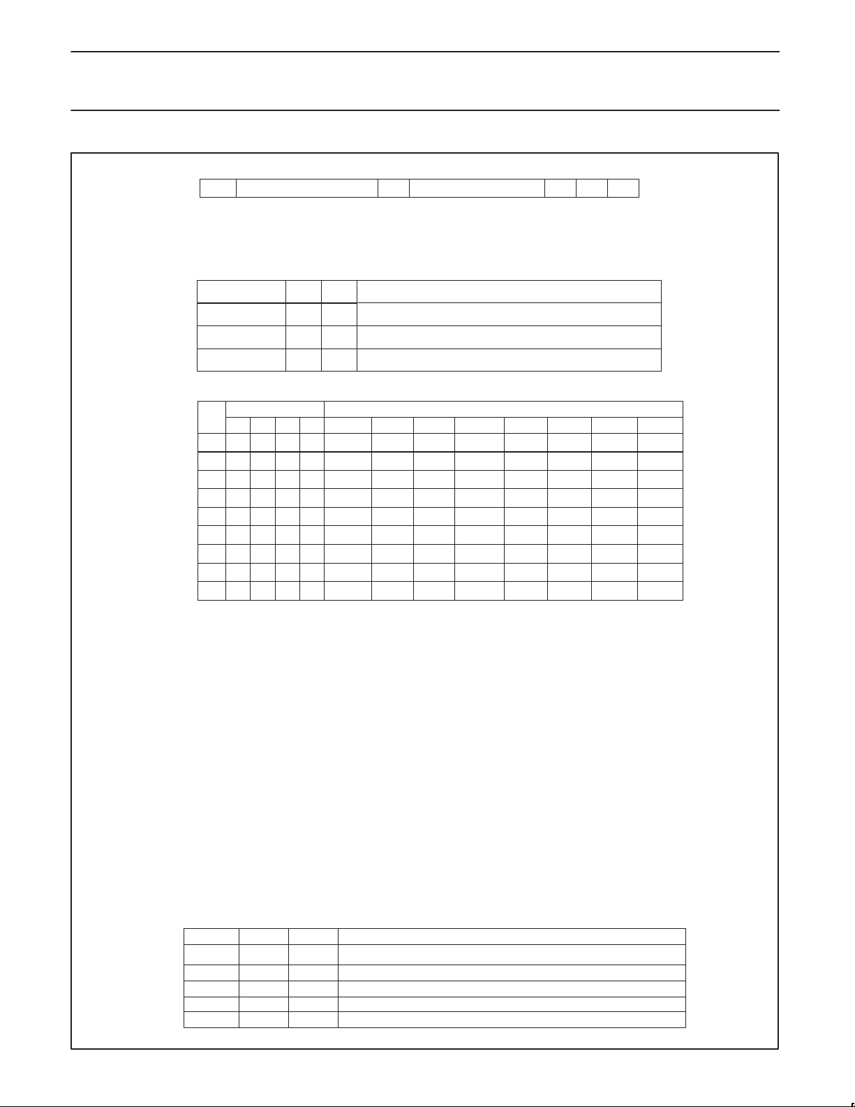
The control register bit map is shown below. Either a quick access
or normal address mode can be used, determined by the two MSB
bits in the first word following the SA5753 address word. If the quick
access mode is used, the registers R0 or R1 can be updated by
sending only two bytes of information (address plus update). If R0
or R1 are updated using the address mode, then B7 and B6 of the
data word are ignored. In all access modes, incremental register
addressing is supported with following words updating the next
register until a ‘stop’ bit is sent.
High Tone DTMF Register
MSB LSB
HD7 HD6 HD5 HD4 HD3 HD2 HD1 HD0
The eight bits determine the output frequency by the following
formula.:
High Frequency = 1200kHz/6/HD
where HD is the value of the register.
Low Tone DTMF Register
MSB LSB
LD7 LD6 LD5 LD4 LD3 LD2 LD1 LD0
The eight bits determine the output frequency by the following
formula.:
Low Frequency = 1200kHz/14/LD
where LD is the value of the register.
The operation of the 96ms DTMF timer is initiated by the loading of
the low tone DTMF register. This timer terminates transmission of
the tones as the generated tones cross the reference level after
96ms. The on time of the tones can thus vary by up to one cycle of
the tones.
Continuous tones can be obtained by again loading DTC = 1 in R1,
bit 5.
Single tones can be obtained by loading 2 into the unused tone
register to silence it.
Loading a value of 1 or 0 into the registers will default the register
value to 257 or 256 for high tone or low tone, respectively.
Phase continuous frequency modulation can be produced by loading
a new value into a DTMF register during continuous operation
(DTC=1).
1997 Nov 07
7
Page 8
Philips Semiconductors Product specification
SA5753Audio processor – filter and control section
2
C Address and Access
I
S A7 A6 A5 A4 A3 A2 A1 A0 ACK ACK
F7 F6 F5 F4 F3 F2 F1 F0 ... P
S = start, A0 = 0, ACK = acknowledge, P = stop, A7–0 = SA5753 address fixed internally at 1000000.
Access mode is determined by F7, F6.
All access modes support incremental addressing.
Mode F7 F6
quick access 0
quick access
test mode
address mode
Load F5–F0 to R0B5 – R0B0
0
0
1
1
Load F5-F0 to R1B5 – R1B0
1
For test only. DO NOT USE.
0
F3–F0 point to register
1
Action
Address Map
REG
R0 0 0
R1
R2
R3
R4
R5
R6
R7
Address
F3 F2
0
0
0
0
0
0
0
0
0
0
1
1
1
1
F1 F0
00
0
1
1
0
1
1
0
0
0
1
1
0
1
1
R81000
B7 B6 B5 B4 B3 B2 B1 B0
Y
Y
HD7
LD7
A1b3
A6b3
A2ab4
A3b3
VOX
CTL
Y
Y
HD6
LD6
A1b2
A6b2
A2ab3
A3b2
S3
RxM
DTC
HD5
LD5
A1b1
A6b1
A2ab2
A3b1
S5
Register Bits
TxM
S4
HD4
LD4
A1b0
A6b0
A2ab1
A3b0
S6
A2bb1
S8
HD3
LD3
A4b3
NAMPS
A2ab0
A7b3
S11
A2bb0
S13
HD2
LD2
A4b2
VCO
PWDN
A7b2
RxP
S9
S7
HD1
LD1
A4b1
HPDN
IDLE 1
A7b1
TxP
S10
S2
HD0
LD0
A4b0
S12
IDLE 0
A7b0
S1
Y = ignored in address mode.
For all bits TRUE = ‘1’
A1b3–0 = program bits for gain block A1
A2ab4–0 = program bits for gain block A2a
A2bb1–0 = program bits for gain block A2b
A3b3–0 = program bits for gain block A3
A4b4–0 = program bits for gain block A4
A5b2–0 = program bits for gain block A5
A6b3–0 = program bits for gain block A6
A7b3–0 = program bits for gain block A7
HD7–0 = high tone DTMF
LD7–0 = low tone DTMF
NAMPS = program bit for NAMPS offset
VCO = 6dB higher TX
RxM = receive mute
OUT
TxM = transmit mute
RxP = receive mute polarity
VOX
HPDN = enable power down of compandor circuit. This bit appears at the HPDN pin (Pin 6) of the SA5753
= enable VOX of compandor/expander circuit. This bit appears at the VOX
CTL
TxP = transmit mute polarity
DTC = DTMF continuous
S1 = bypass TXBPF
S2 = bypass compressor in TX path, inhibit pre-emph input
S3 = bypass pre-emp and limiter in Tx path
S4 = enable DTMF to TX path and inhibit PREMPIN and S2.
S5 = bypass RXBPF
S6 = bypass de-emph in RX path
S7 = bypass expandor in RX path, inhibit audio input
S8 = enable DTMF to RX path and inhibit AUDIO
S9 = enable SPKR
S10 = enable EAR
S11 = bypass TXLPF
OUT
OUT
S12 = cordless data option established
S13 = enable data path
pin (Pin 5) of the SA5753.
CTL
PWDN, IDLE1, IDLE0 see Table below
Low Power Modes (R6B0 – R6B2)
PWDN
IDLE1
1
0
0
0
0
IDLE0
2
X
1
1
0
0
X
(PWDN) Complete power down except I
(DENA) Low power, I/Os at V
0
(IDLE) Low power, I/Os at V
1
Normal operation.
0
1
IN
to TX
DATA
OUT
disabled.
/2, DATAIN to TX
DD
/2, DATAIN to TX
DD
C, I/Os high impedance.
enabled.
OUT
disabled.
OUT
X = don’t care.
and S7.
IN
SR00667
1997 Nov 07
8
Page 9
Philips Semiconductors Product specification
SA5753Audio processor – filter and control section
220nF
TXBF
TXBF
PREMP
VOX
IN
OUT
CTL
S12
S11
220nF
1
S12
220nF
33nF
IN
V
DD
.1µF
2
3
4
5
S1
TXBPF
I2C R8B7
S2
ATTN 1
S2
S3
S4
TXLPF
PREEMPH
AND
SOFT LIM
ATTN 2
S4
MUTE
TX
2
I
AND
REGISTERS
S13
ATTN 3
C INTERFACE
Σ
V
REF
I2C R0B4
ATTN 4
I2C R8B1
20
33nF
19
18
17
16
TX
OUT
DATA
IN
TX MUTE
SDA
SCL
HPDN
DEMP
AUDIO
SPEAKER
EAR
OUT
OUT
OUT
6
2.2µF
7
220nF
IN
220nF
220nF
8
9
10
I2C R5B1
S7
S7
S9
S10
S6
DEEMPH
S8
S8
ATTN 6
S5
DTMF
GEN
RXBPF
MUTE
RX
ATTN 7
I2C R0B5
I2C R8B3
15
14
13
12
11
GND
220nF
1.2MHz
CLK
IN
DFT
RX MUTE
RX DEMOD
IN
1997 Nov 07
SR00668
Figure 2. SA5753 Test and Application Circuit
9
Page 10
Philips Semiconductors Product specification
SA5753Audio processor – filter and control section
TX
OUT
ATTN 6
220nF
RX DEMOD
11
ATTN 7
S10
10
EAR OUT
C15
220nF
IN
SA5753
TDA7050T
GND
S6
HPDN
13
IN
1.2MHz
CLOCK
14
DEEMPH
S7
7
DE EMPH OUT
C8
+
IN
EXP
12
S8
2.2 Fµ
DFT
13
RXBPF
S5
S8
S7
8
AUDIO IN
C7
220nF
11
MUTE
RX
12
I2C R8B3
Rx MUTE R0B5
RX
MUTE
S9
9
SPKR OUT
C16
OUT
EXP
IN
19
ATTN 3
PREEMPH
C12
220nF
MUTE
TX
18
AND
SOFT LIM
S3
PRE EMPH IN
CAP3
COMP
220nF
18
I2C R8B1
3
C11
20
REF
V
S13
ATTN 1
2
TXBPF OUT
IN
COMP
220nF
C13
19
DATA
20
ATTN 4
Σ
S12
TX
MUTE
S11
TXLPF
S1
TXBPF
S12
1
TXBPF IN
OUT
SIDE TONE
NCAN
C14
SDA
17
Tx MUTE R0B4
ATTN 2
S2
4
DD
V
33nF
C10
CAP3
COMP
COMP
+
2.2 Fµ
17
OUT
16
SCL
16
2
I C INTERFACE
S4
S4
S2
I2C R8B7
5
CTL
VOX
0.1 Fµ
CAP2
2.2 Fµ
+
COMP
C9
15
AND
REGISTERS
I2C R5B1
6
HPDN
CTL
VOX
14
15
GEN
DTMF
1997 Nov 07
NOISE
PREAMP
1
C1
IN
MIC
BUFFER
CANCEL
C2
220nF
COMP
2
+
4.7 Fµ
GRES
R1
PREAMP
Avset
R2
RECT
3
43k
GRES
VOX
22nF
C3
C4
2.2 Fµ
4
+
CAP
NCAN
R3
4.3k
5
OUT
VOX
6
7
R4
5.6k
TR
GND
VOX
BANDGAP
8
+
REF
V
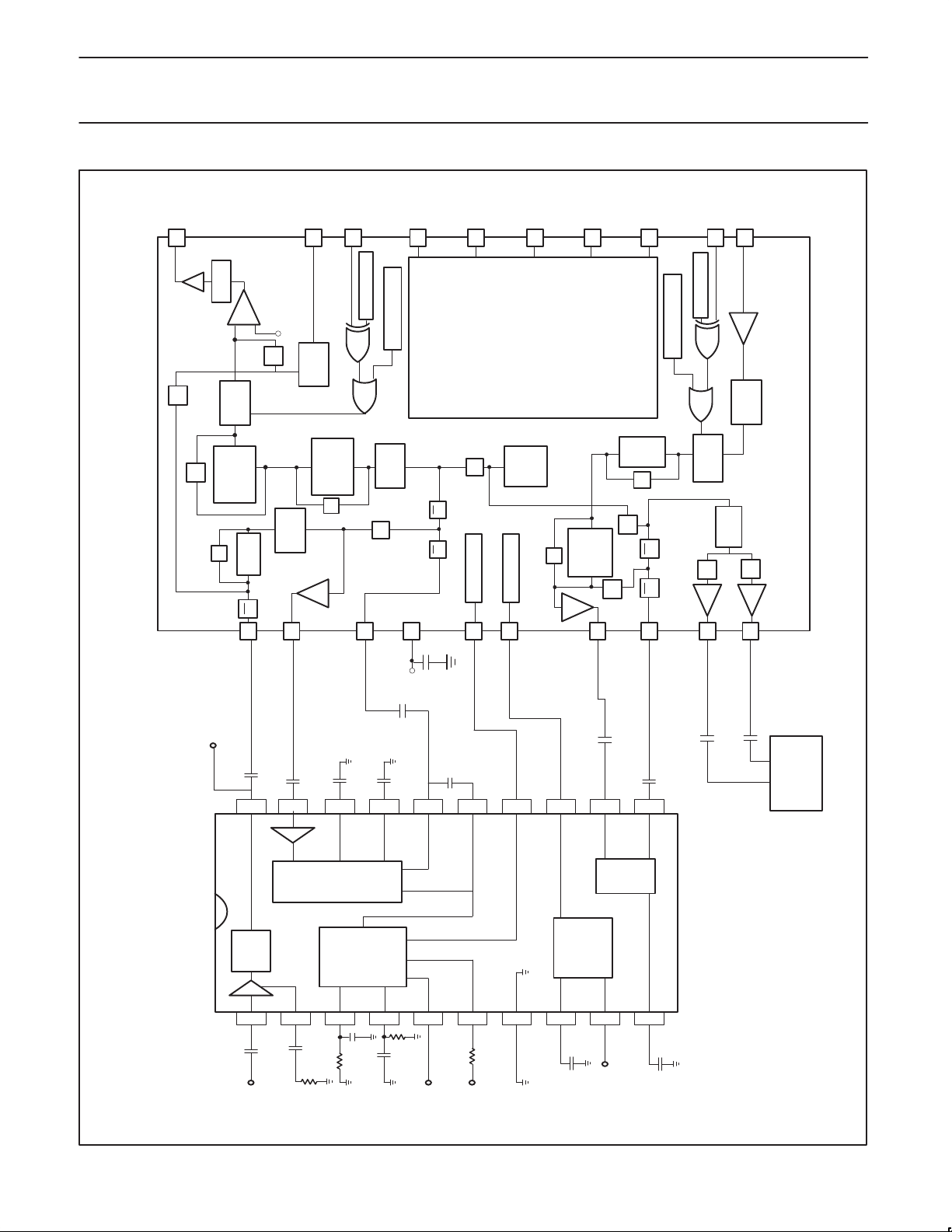
Figure 3. Application Diagram for the Audio Processor
10
C5
VOLTAGE
10 Fµ
REF
V
EXP
SA5752
9
10
C6
+
CC
CAP
EXP
2.2 Fµ
SR00669
Page 11
Philips Semiconductors Product specification
SA5753Audio processor – filter and control section
Companding and Amplifier Section Filter and Control Section
SA5753SA5752
MICROPHONE
GAIN
CONTROL
VOX
OUTPUT
HEADPHONE
SPEAKER
PREAMP
VOX
PA
CANCEL
COMPRESSOR
EXPANDOR
TDA7050T
NOISE
TX
BANDPASS
FILTER
TX
PRE–
EMPHASIS
RX
DE–
EMPHASIS
ATTENUATOR
PA
SUMMING
AMP
TX
LOW
PASS
FILTER
RX
BANDPASS
FILTER
DTMF
GENERATOR
2
C
I
BUS
INTERFACE
VOX CONTROL
AUDIO TO
TRANSMITTER
AUDIO FROM
RECEIVER
DEMODULATOR
CLOCK
1.2MHz
FROM SYSTEM
CONTROLLER I C BUS
2
1997 Nov 07
SR00661
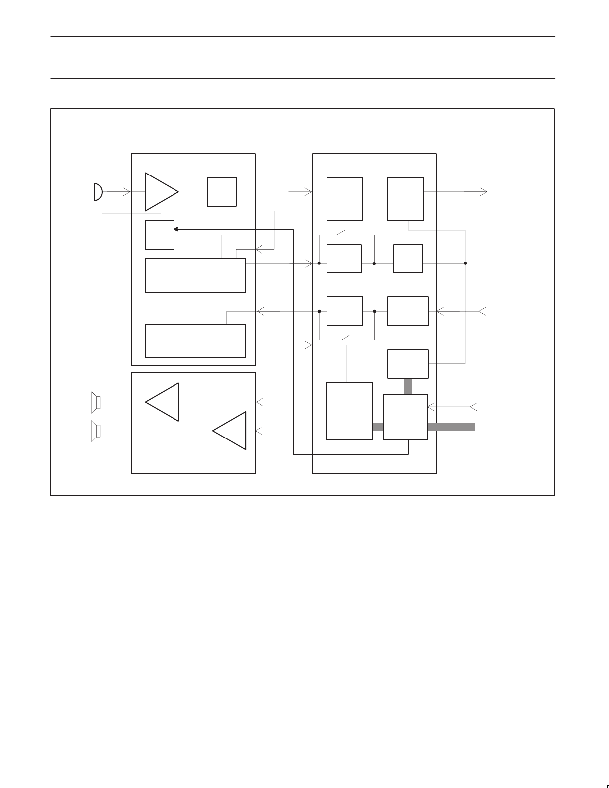
Figure 4. Typical Configuration of Audio Processor (APROC) System Chip Set
11
Page 12
Philips Semiconductors Product specification
SA5753Audio processor – filter and control section
DEMOD DATA
DATA PROCESSOR
POWER SUPPLY
RF BLOCK
TXEN
DEMOD
MOD
SA5752
TDA7050
DATA
SA5753
LOGIC UNIT
POWER SUPPLY ENABLE
VOX
MIC
EAR
SPEAKER
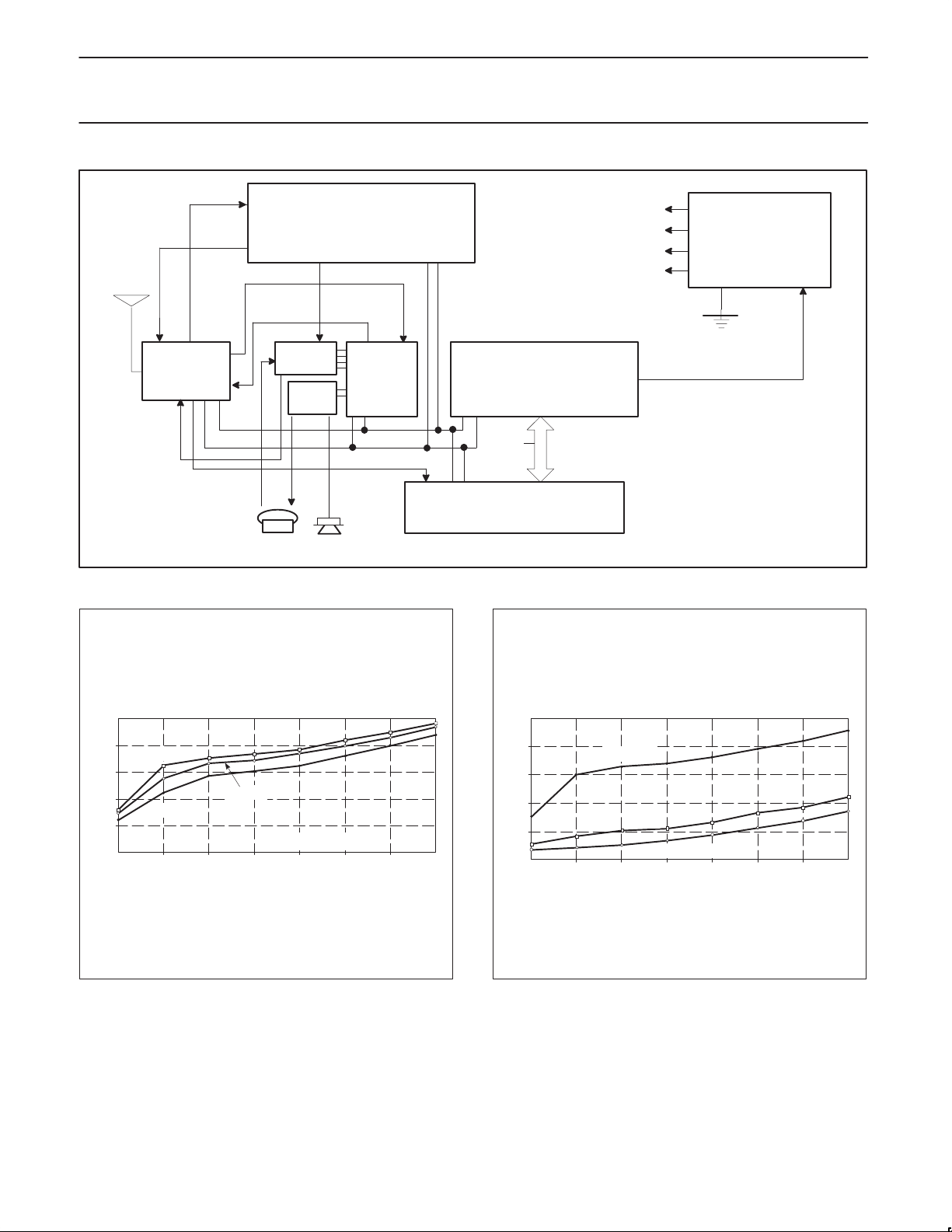
Figure 5. APROC Application Diagram
2.5
2
1.5
1
Icc (mA)
0.5
0
+85°C
+25°C
-40°C
ICC vs VCC vs TEMP
2 2.5 3 3.5 4 4.5 5 5.5
VCC (V)
I2C
8
CONTROL UNIT
2.5
2
1.5
Icc (mA)
1
0.5
0
2 2.5 3 3.5 4 4.5 5 5.5
SR00670
NORMAL
IDLE
POWER DOWN
VCC (V)
1997 Nov 07
Figure 6. SA5753 Normal Operation
SR00671
SR00672
Figure 7. SA5753 Power Mode Comparison (ICC)
12
Page 13
Philips Semiconductors Product specification
SA5753Audio processor – filter and control section
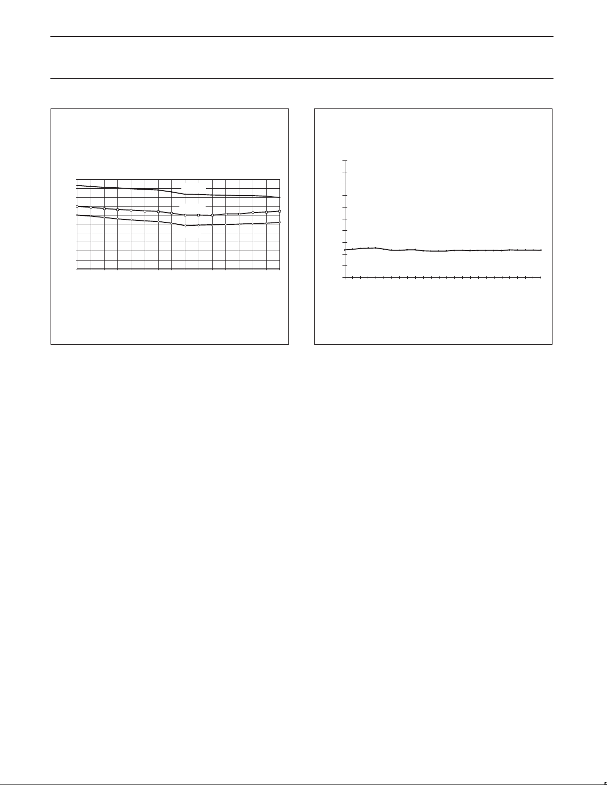
1000
NOISE LEVEL (uV)
900
800
700
600
500
400
300
200
100
0
2.5
2.6
2.7
2.8
2.9
3.0
3.1
3.2
3.3
3.4
3.5
3.6
3.7
3.8
3.9
4.0
4.1
4.2
4.3
4.4
4.5
4.6
4.7
4.8
4.9
POWER SUPPLY (V)
5.0
1
0.8
0.6
0.4
0.2
0
-0.2
-0.4
ERROR (dB)
-0.6
-0.8
-1
-28 -26 -24 -22 -20 -18 -16 -14 -12 -10 -8 -6 -4 -2 0
-30
ATTENUATION LEVEL (dB)
-40°C
+25°C
+85°C
Figure 8. Gain Control, A6 Linearity
SR00673
SR00674
Figure 9. Power Supply vs Noise at TXBPF (25°C)
1997 Nov 07
13
Page 14
Philips Semiconductors Product specification
SA5753Audio processor — filter and control section
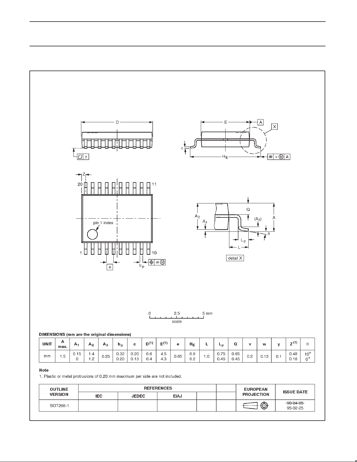
SSOP20: plastic shrink small outline package; 20 leads; body width 4.4 mm SOT266-1
1997 Nov 07
14
Page 15

Philips Semiconductors Product specification
SA5753Audio processor — filter and control section
DEFINITIONS
Data Sheet Identification Product Status Definition
Objective Specification
Preliminary Specification
Product Specification
Formative or in Design
Preproduction Product
Full Production
Philips Semiconductors and Philips Electronics North America Corporation reserve the right to make changes, without notice, in the products,
including circuits, standard cells, and/or software, described or contained herein in order to improve design and/or performance. Philips
Semiconductors assumes no responsibility or liability for the use of any of these products, conveys no license or title under any patent, copyright,
or mask work right to these products, and makes no representations or warranties that these products are free from patent, copyright, or mask
work right infringement, unless otherwise specified. Applications that are described herein for any of these products are for illustrative purposes
only. Philips Semiconductors makes no representation or warranty that such applications will be suitable for the specified use without further testing
or modification.
LIFE SUPPORT APPLICA TIONS
Philips Semiconductors and Philips Electronics North America Corporation Products are not designed for use in life support appliances, devices,
or systems where malfunction of a Philips Semiconductors and Philips Electronics North America Corporation Product can reasonably be expected
to result in a personal injury. Philips Semiconductors and Philips Electronics North America Corporation customers using or selling Philips
Semiconductors and Philips Electronics North America Corporation Products for use in such applications do so at their own risk and agree to fully
indemnify Philips Semiconductors and Philips Electronics North America Corporation for any damages resulting from such improper use or sale.
Philips Semiconductors
811 East Arques Avenue
P.O. Box 3409
Sunnyvale, California 94088–3409
Telephone 800-234-7381
This data sheet contains the design target or goal specifications for product development. Specifications
may change in any manner without notice.
This data sheet contains preliminary data, and supplementary data will be published at a later date. Philips
Semiconductors reserves the right to make changes at any time without notice in order to improve design
and supply the best possible product.
This data sheet contains Final Specifications. Philips Semiconductors reserves the right to make changes
at any time without notice, in order to improve design and supply the best possible product.
Copyright Philips Electronics North America Corporation 1997
All rights reserved. Printed in U.S.A.
1997 Nov 07
15
 Loading...