

Page 1

RF COMMUNICATIONS PRODUCTS
SA575
Low voltage compandor
Product specification
Replaces data of 1997 June 28
IC17
Philips Semiconductors
1997 Nov 07
Page 2
Philips Semiconductors Product specification
SYMBOL
PARAMETER
UNITS
SA575Low voltage compandor
DESCRIPTION
The SA575 is a precision dual gain control circuit designed for low
voltage applications. The SA575’s channel 1 is an expandor, while
channel 2 can be configured either for expandor, compressor, or
automatic level controller (ALC) application.
FEA TURES
•Operating voltage range from 3V to 7V
•Reference voltage of 100mV
RMS
= 0dB
•One dedicated summing op amp per channel and two extra
uncommitted op amps
•600Ω drive capability
•Single or split supply operation
•Wide input/output swing capability
•3000V ESD protection
APPLICATIONS
•Portable communications
•Cellular radio
•Cordless telephone
•Consumer audio
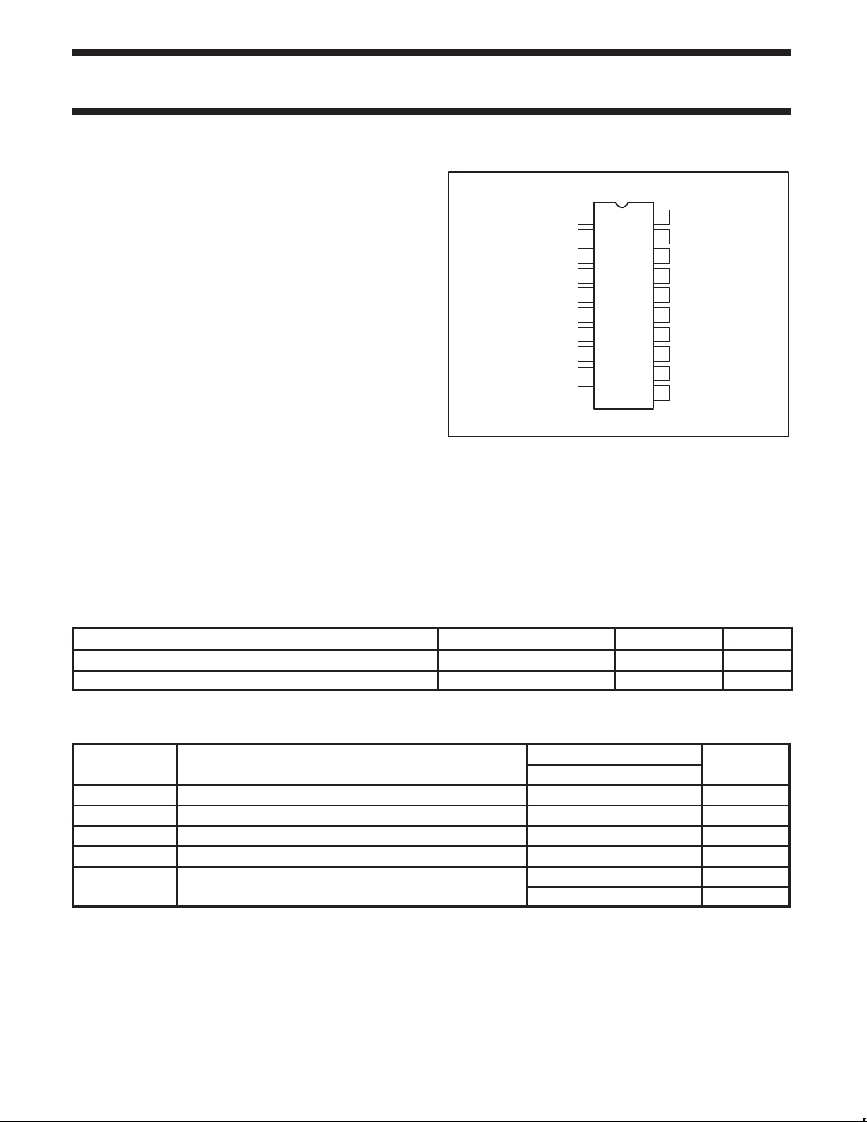
PIN CONFIGURATION
D1 and DK Packages
1
+V
IN1
2
-V
IN1
3
V
OUT
1
RECT1
V
REF
GND
4
5
6
7
8
9
10
RECT. IN1
C
SUM OUT 1
COMP. IN1
GAIN CELL IN1
NOTE:
1. Available in large SOL package only.
Figure 1. Pin Configuration
•Portable broadcast mixers
•Wireless microphones
•Modems
•Electric organs
•Hearing aids
20 V
CC
19 +V
IN2
18 -V
IN2
17 V
OUT2
16 RECT.IN2
15 C
RECT2
14 SUM OUT2
13 COMP.IN2
12 SUM NODE 2
11 GAIN CELL IN2
SR00703
ORDERING INFORMATION
DESCRIPTION TEMPERATURE RANGE ORDER CODE DWG
20-Pin Plastic Small Outline Large -40 to +85°C SA575D SOT163-1
20-Pin Plastic Shrink Small Outline Package (SSOP) -40 to +85°C SA575DK SOT266-1
ABSOLUTE MAXIMUM RATINGS
RATING
SA575
T
V
V
θ
CC
IN
T
A
STG
JA
Single supply voltage –0.3 to 8 V
Voltage applied to any other pin –0.3 to (VCC+0.3) V
Operating ambient temperature range -40 to +85 °C
Storage temperature range -65 to +150 °C
Thermal impedance SOL 112 °C/W
SSOP 117 °C/W
1997 Nov 07 853-1665 18666
2
Page 3
Philips Semiconductors Product specification
SA575Low voltage compandor
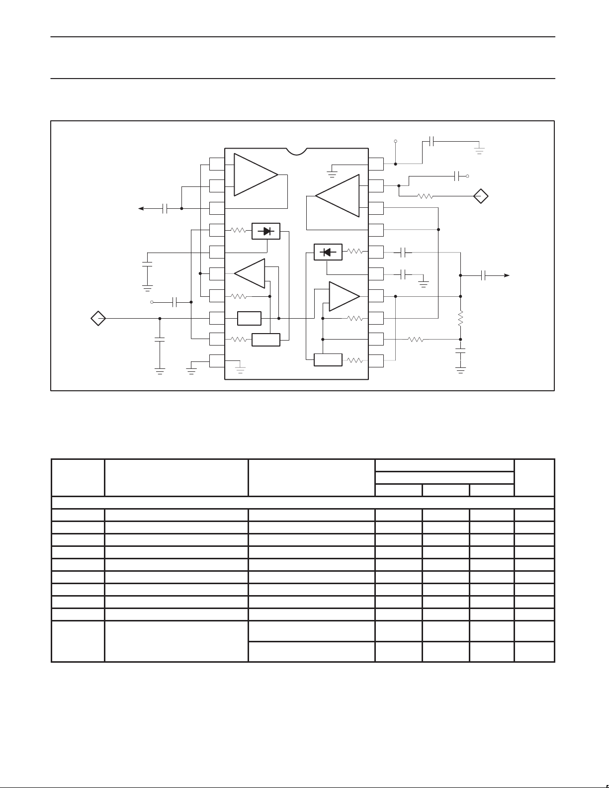
BLOCK DIAGRAM and TEST CIRCUIT
0.1µF
+5V
V
CC
V
REF
V
OUT
GND
V
+
IN
GND
+
C3
10µF
C
RECT
2.2µF
10µF
+
C6
10µF
+
GND
+
1
2
–
OP AMP
3
4
3.8k
575
OP AMP
V
CC
5
10k
10k
V
Σ
Σ
REF
∆G
∆G
GND
6
7
8
9
10
Figure 2. Block Diagram and Test Circuit
+
–
3.8k
10k
10k
20
19
18
17
16
15
14
13
12
11
C
RECT
C11
+
2.2µF
+
4.7µF
R7
30k
R13
10k
C15
C8
10µF
+
C14
+
R8
30k
GND
1µF
V
+
IN
C10
10µF
GND
V
REF
V
OUT
SR00704
DC ELECTRICAL CHARACTERISTICS
Typical values are at TA = 25°C. Minimum and Maximum values are for the full operating temperature range: -40 to +85°C for SA575, except
SSOP package is tested at +25°C only. V
SYMBOL PARAMETER TEST CONDITIONS SA575 UNITS
For compandor, including summing amplifier
V
CC
I
CC
V
REF
R
Supply voltage
Supply current No signal 3 4.2 5.5 mA
Reference voltage
Summing amp output load 10 kΩ
L
1
2
THD Total harmonic distortion 1kHz, 0dB BW = 3.5kHz 0.12 1.5 %
E
NO
Output voltage noise BW = 20kHz, RS = 0Ω 6 30 µV
0dB Unity gain level 1kHz -1.5 1.5 dB
V
OS
Output voltage offset No signal -150 150 mV
Output DC shift No signal to 0dB -100 100 mV
Tracking error relative to 0dB
= 5V, unless otherwise stated. Both channels are tested in the Expandor mode (see Test Circuit)
CC
LIMITS
MIN TYP MAX
3 5 7 V
VCC = 5V 2.4 2.5 2.6 V
Gain cell input = 0dB, 1kHz
Rectifier input = 6dB, 1kHz
Gain cell input = 0dB, 1kHz
Rectifier input = -30dB, 1kHz
-1.0 1.0 dB
-1.0 1.0 dB
1997 Nov 07
3
Page 4

Philips Semiconductors Product specification
SA575Low voltage compandor
DC ELECTRICAL CHARACTERISTICS (cont.)
LIMITS
SYMBOL PARAMETER TEST CONDITIONS SA575 UNITS
MIN TYP MAX
Crosstalk 1kHz, 0dB, C
For operational amplifier
V
O
R
Output swing RL = 10kΩ VCC-0.4 V
Output load 1kHz 600 Ω
L
CMR Input common-mode range 0 V
CMRR Common-mode rejection ratio 60 80 dB
A
V
VOL
I
B
OS
Input bias current VIN = 0.5V to 4.5V -1 1 µA
Input offset voltage 3 mV
Open-loop gain RL = 10kΩ 80 dB
SR Slew rate Unity gain 1 V/µs
GBW Bandwidth Unity gain 3 MHz
E
NI
Input voltage noise BW = 20kHz 2.5 µV
PSRR Power supply rejection ratio 1kHz, 250mV 60 dB
NOTES:
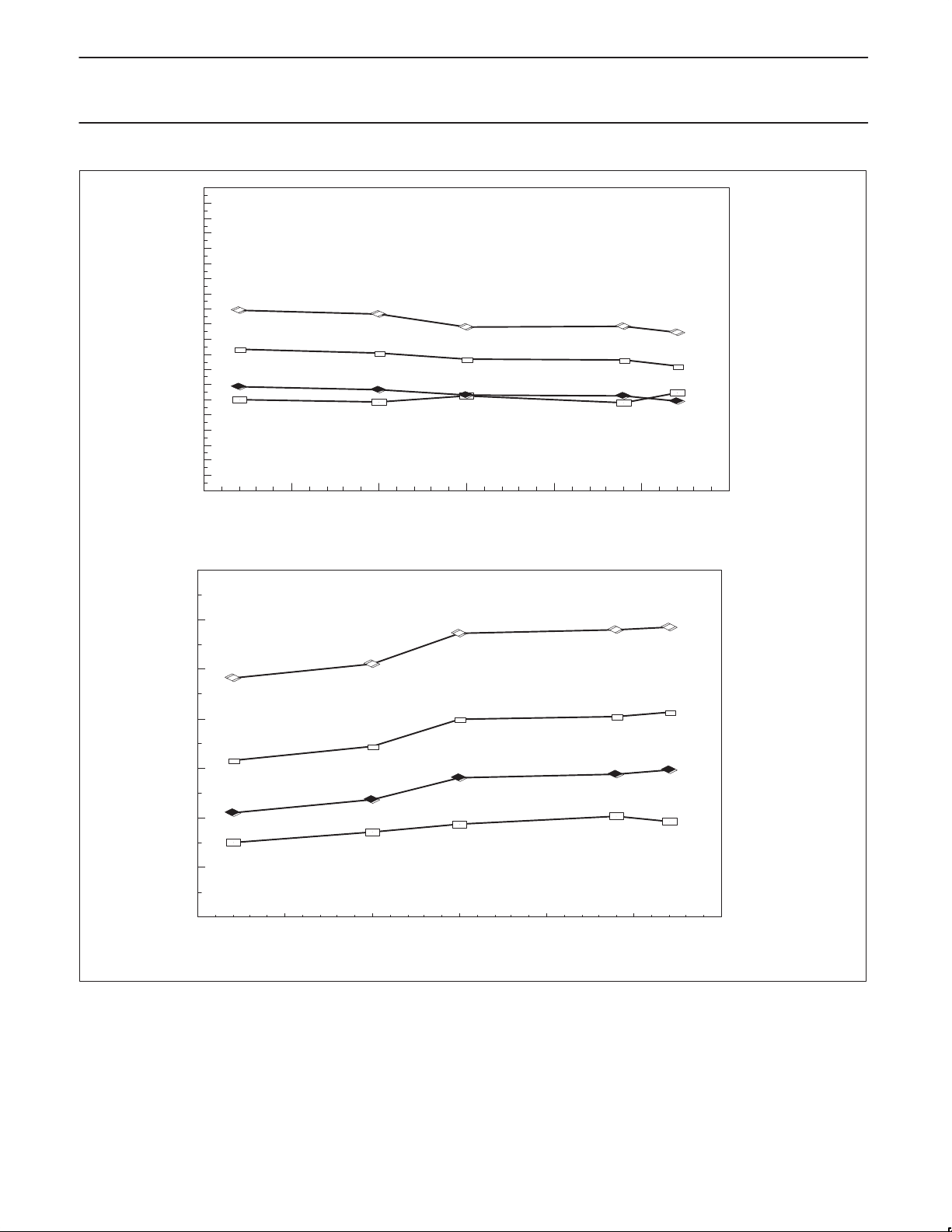
1. Operation down to V
2. Reference voltage, V
= 2V is possible, but performance is reduced. See curves in Figure 7a and 7b.
CC
, is typically at 1/2VCC.
REF
FUNCTIONAL DESCRIPTION
This section describes the basic subsystems and applications of the
SA575 Compandor. More theory of operation on compandors can
be found in AN174 and AN176. The typical applications of the
SA575 low voltage compandor in an Expandor (1:2), Compressor
(2:1) and Automatic Level Control (ALC) function are explained.
These three circuit configurations are shown in Figures 3, 4, 5
respectively.
The SA575 has two channels for a complete companding system.
The left channel, A, can be configured as a 1:2 Expandor while the
right channel, B, can be configured as either a 2:1 Compressor, a
1:2 Expandor or an ALC. Each channel consists of the basic
companding building blocks of rectifier cell, variable gain cell,
summing amplifier and V
additional high performance uncommitted op amps which can be
utilized for application such as filtering, pre-emphasis/de-emphasis
or buffering.
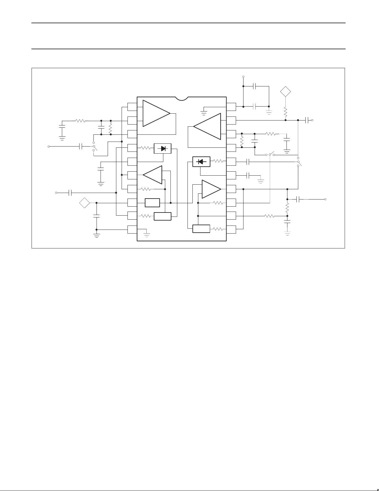
Figure 6 shows the complete schematic for the applications demo
board. Channel A is configured as an expandor while channel B is
configured so that it can be used either as a compressor or as an
ALC circuit. The switch, S1, toggles the circuit between compressor
and ALC mode. Jumpers J1 and J2 can be used to either include
the additional op amps for signal conditioning or exclude them from
the signal path. Bread boarding space is provided for R1, R2, C1,
C2, R10, R11, C10 and C11 so that the response can be tailored for
each individual need. The components as specified are suitable for
the complete audio spectrum from 20Hz to 20kHz.
The most common configuration is as a unity gain non-inverting
buffer where R1, C1, C2, R10, C10 and C11 are eliminated and R2
and R11 are shorted. Capacitors C3, C5, C8, and C12 are for DC
blocking. In systems where the inputs and outputs are AC coupled,
these capacitors and resistors can be eliminated. Capacitors C4
and C9 are for setting the attack and release time constant.
C6 is for decoupling and stabilizing the voltage reference circuit.
The value of C6 should be such that it will offer a very low
impedance to the lowest frequencies of interest. Too small a
capacitor will allow supply ripple to modulate the audio path. The
cell. In addition, the SA575 has two
REF
= 220µF -80 -65 dB
REF
CC
CC
V
V
better filtered the power supply, the smaller this capacitor can be.
R12 provides DC reference voltage to the amplifier of channel B.
R6 and R7 provide a DC feedback path for the summing amp of
channel B, while C7 is a short-circuit to ground for signals. C14 and
C15 are for power supply decoupling. C14 can also be eliminated if
the power supply is well regulated with very low noise and ripple.
DEMONSTRATED PERFORMANCE
The applications demo board was built and tested for a frequency
range of 20Hz to 20kHz with the component values as shown in
Figure 6 and V
= 5V. In the expandor mode, the typical input
CC
dynamic range was from -34dB to +12dB where 0dB is equal to
100mV
input was +
. The typical unity gain level measured at 0dB @ 1kHz
RMS
0.5dB and the typical tracking error was +0.1dB for input
range of -30 to +10dB.
In the compressor mode, the typical input dynamic range was from
-42dB to +
gain level was +
18dB with a tracking error +0.1dB and the typical unity
0.5dB.
In the ALC mode, the typical input dynamic range was from -42dB to
+8dB with typical output deviation of +
0.2dB about the nominal
output of 0dB. For input greater than +9dB in ALC configuration, the
summing amplifier sometimes exhibits high frequency oscillations.
There are several solutions to this problem. The first is to lower the
values of R6 and R7 to 20kΩ each. The second is to add a current
limiting resistor in series with C12 at Pin 13. The third is to add a
compensating capacitor of about 22 to 30pF between the input and
output of summing amplifier (Pins 12 and 14). With any one of the
above recommendations, the typical ALC mode input range
increased to +18dB yielding a dynamic range of over 60dB.
EXPANDOR
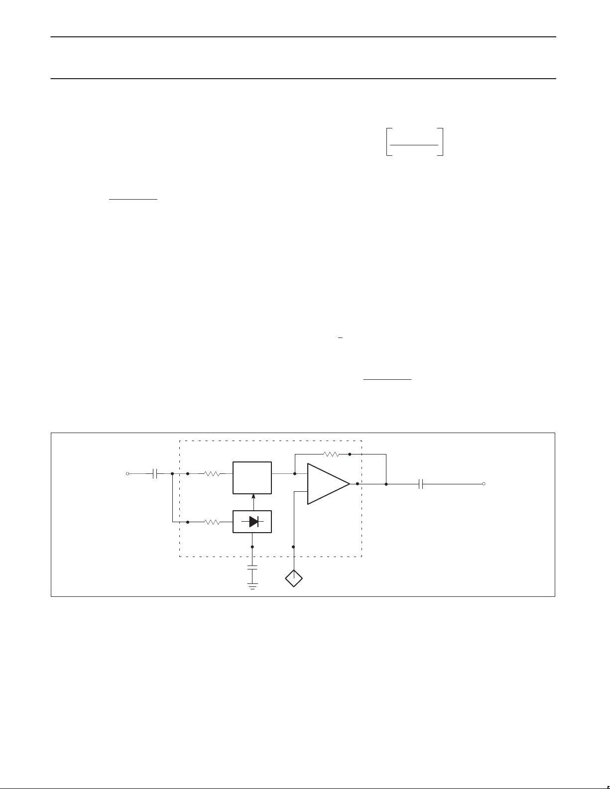
The typical expandor configuration is shown in Figure 3. The
variable gain cell and the rectifier cell are in the signal input path.
The V
without clipping. The 0dB ref is 100mV
coupled through C5, and the output is AC coupled through C3. If in
a system the inputs and outputs are AC coupled, then C3 and C5
can be eliminated, thus requiring only one external component, C4.
The variable gain cell and rectifier cell are DC coupled so any offset
is always 1/2 VCC to provide the maximum headroom
REF
. The input is AC
RMS
1997 Nov 07
4
Page 5
Philips Semiconductors Product specification
SA575Low voltage compandor
voltage between Pins 4 and 9 will cause small offset error current in
the rectifier cell. This will affect the accuracy of the gain cell. This
can be improved by using an extra capacitor from the input to Pin 4
and eliminating the DC connection between Pins 4 and 9.
The expandor gain expression and the attack and release time
constant is given by Equation 1 and Equation 2, respectively.
Equation 1.
4V
(avg)
Expandor gain =
where VIN(avg) = 0.95V
IN
3.8k x 100µA
IN(RMS)
Equation 2.
τR = τA = 10k x C
RECT
= 10k x C4
COMPRESSOR
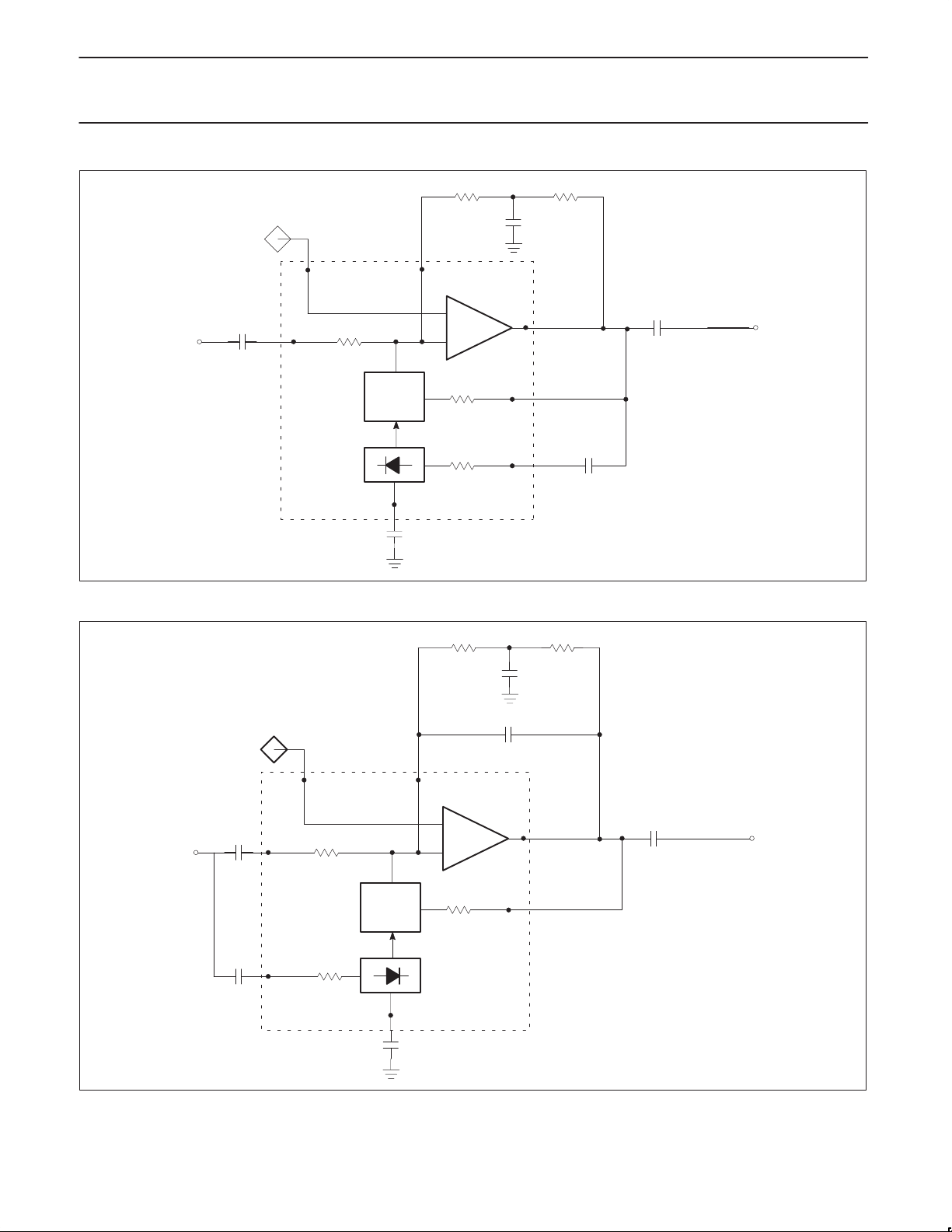
The typical compressor configuration is shown in Figure 4. In this
mode, the rectifier cell and variable gain cell are in the feedback
path. R6 and R7 provide the DC feedback to the summing amplifier.
The input is AC coupled through C12 and output is AC coupled
through C8. In a system with inputs and outputs AC coupled, C8
and C12 could be eliminated and only R6, R7, C7, and C13 would
be required. If the external components R6, R7 and C7 are
eliminated, then the output of the summing amplifier will motor-boat
in absence of signals or at extremely low signals. This is because
there is no DC feedback path from the output to input. In the
presence of an AC signal this phenomenon is not observed and the
circuit will appear to function properly.
The compressor gain expression and the attack and release time
constant is given by Equation 3 and Equation 4, respectively.
Equation 3.
1/2
IN(RMS)
Compressor gain =
where VIN(avg) = 0.95V
3.8k x 100µA
4V
(avg)
IN
Equation 4.
τR = τA = 10k x C
RECT
= 10k x C4
AUTOMATIC LEVEL CONTROL
The typical Automatic Level Control circuit configuration is shown in
Figure 5. It can be seen that it is quite similar to the compressor
schematic except that the input to the rectifier cell is from the input
path and not from the feedback path. The input is AC coupled
through C12 and C13 and the output is AC coupled through C8.
Once again, as in the previous cases, if the system input and output
signals are already AC coupled, then C12, C13 and C8 could be
eliminated. Concerning the compressor , removing R6, R7 and C7
will cause motor-boating in absence of signals. C
to stabilize the summing amplifier at higher input levels. This circuit
provides an input dynamic range greater than 60dB with the output
within +
0.5dB typical. The necessary design expressions are given
by Equation 5 and Equation 6, respectively.
Equation 5.
ALC gain =
τR = τA = 10k x C
3.8k x 100µA
4V
(avg)
IN
= 10k x C9
RECT
Equation 6.
COMP
is necessary
EXP IN
C5
10µF
7
9
10k
4
3.8k
∆G
5
2.2µF
C4
10k
Σ
8
V
REF
6
C3
EXP OUT
10µF
SR00705
Figure 3. Typical Expandor Configuration
1997 Nov 07
5
Page 6
Philips Semiconductors Product specification
SA575Low voltage compandor
COMP IN
V
REF
C12
10µF
R6
30k
C7
8
13
10k
15
C9
12
Σ
G
∆
10k
3.8k
2.2µF
14
11
R7
30k
1µF
C8
10µF
16
C13
4.7µF
COMP OUT
SR00706
Figure 4. Typical Compressor Configuration
1µF
R7
30k30k
R6
C7
ALC IN
V
REF
C12
10µF
C13
4.7µF
C COMP
22pF
8
13
10k
16
3.8k
16
C9
12
Σ
G
∆
10k
2.2µF
14
11
C8
ALC OUT
10µF
SR00707
Figure 5. Typical ALC Configuration
1997 Nov 07
6
Page 7
Philips Semiconductors Product specification
SA575Low voltage compandor
-5V
V
CC
EXP
OUT
EXP
IN
C1
10µF
C15
0.1µF
R11
C13
C9
2.2µF
C14
47µF
C11
4.7µF
+
R1
C3
10µF
1
2
–
C2
R2
OP AMP
3
J1
4
3.8k
575
V
OP AMP
5
C6
10µF
C4
6
7
8
9
10
10k
10k
V
REF
GND
Σ
Σ
∆
G
∆G
2.2µF
C5
V
REF
CC
+
–
3.8k
10k
10k
20
19
18
17
16
15
14
13
12
11
Figure 6. SA575 Low Voltage Expandor/Compressor/ALC Demo Board
J2
R10
R6
30k
R7
30k
V
REF
R12
10k
C10
S1
C7
1µF
C8
10µF
C12
10µF
ALC
COMP
COMP/
ALC
IN
COMP/
ALC
OUT
SR00708
1997 Nov 07
7
Page 8
Philips Semiconductors Product specification
SA575Low voltage compandor
1.0
0.9
0.8
0.7
0.6
0.5
0.4
0.3
0.2
0.1
0.0
–0.1
–0.2
–0.3
UNITY GAIN ERROR (dB)
–0.4
–0.5
–0.6
–0.7
–0.8
–0.9
–1.0
–50 –25 0 25 50 75 100
VCC 7V
5V
V
CC
3V
V
CC
V
2V
CC
TEMPERATURE (°C)
a. Unity Gain Error vs Temperature and V
4.4
4.2
4.0
VCC 7V
3.8
(mA)
CC
I
3.6
3.4
3.2
3.0
–50 –25 0 25 50 75 100
VCC 5V
V
3V
CC
2V
V
CC
TEMPERATURE (°C)
b. ICC vs Temperature and V
CC
CC
Figure 7. Temperature and VCC Curves
SR00709
1997 Nov 07
8
Page 9
Philips Semiconductors Product specification
SA575Low voltage compandor
TYPICAL PERFORMANCE CHARACTERISTICS
GENERAL DIAGRAM
8
10µF
4.7µF
6
4
2
0
–2
–4
–6
–8
–10
OUTPUT LEVEL (dB)
–12
–14
–16
–18
–20
10dB IN
0dB IN
-40dB IN
INPUT
(20–20kHz)
REC
G
∆
SUM
OUTPUT
V
= 5V
CC
–22
10 100 1000 10000 30000
1997 Nov 07
FREQUENCY (Hz)
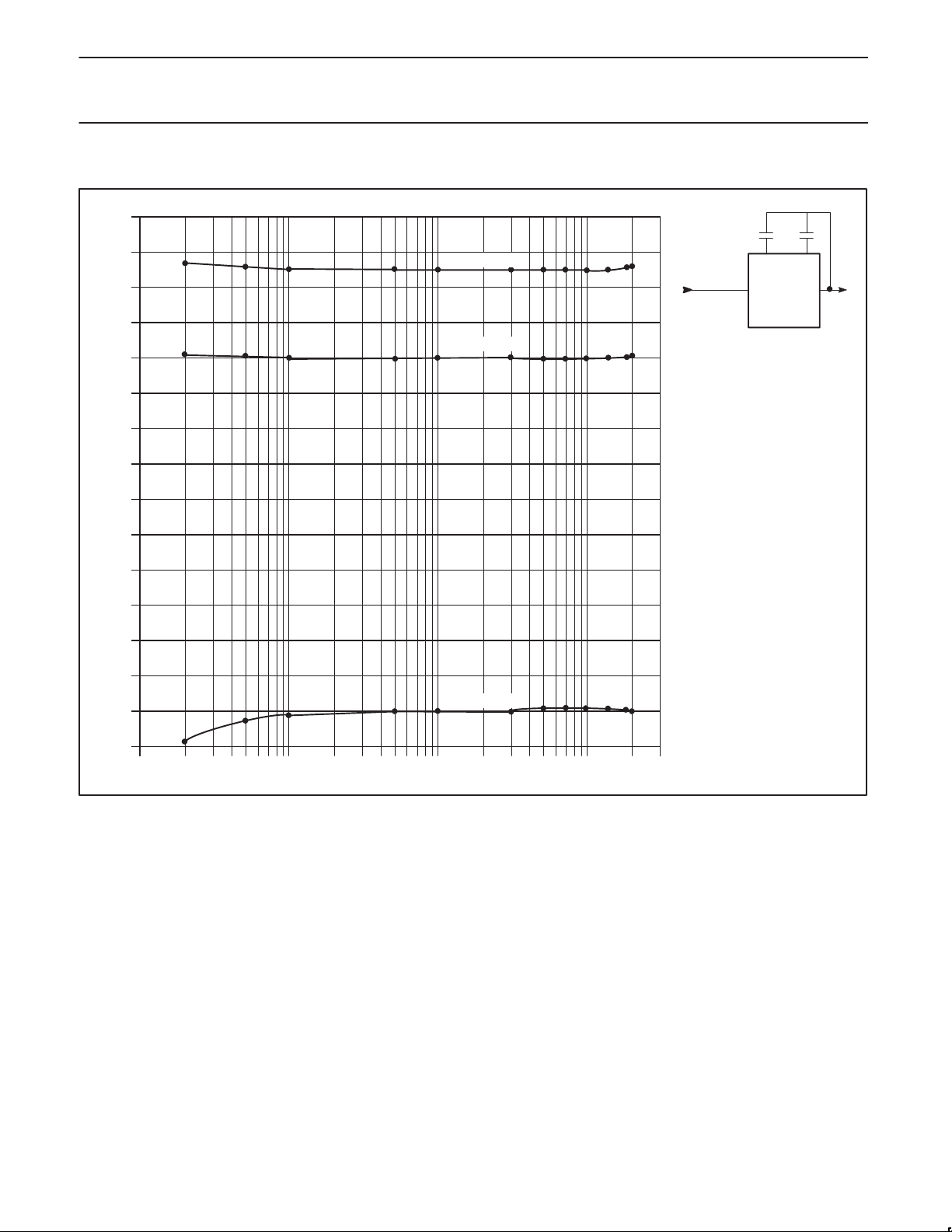
Figure 8. Compressor Output Frequency Response
9
SR00710
Page 10
Philips Semiconductors Product specification
SA575Low voltage compandor
TYPICAL PERFORMANCE CHARACTERISTICS (continued)
–2
–4
–6
–8
–10
OUTPUT LEVEL (dB)
–12
–14
–16
8
6
4
2
0
2.5dB IN
0dB IN
INPUT
(20–20kHz)
GENERAL DIAGRAM
4.7µF
REC
∆
10µF
G
OUTPUT
SUM
= 5V
V
CC
–18
-10dB IN
–20
–22
10 100 1000 10000 30000
FREQUENCY (Hz)
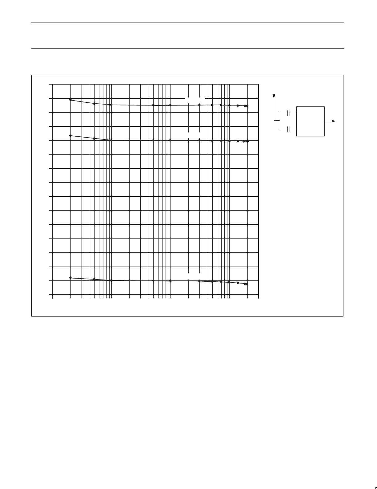
Figure 9. Expandor Output Frequency Response
SR00711
1997 Nov 07
10
Page 11

Philips Semiconductors Product specification
SA575Low voltage compandor
COMPRESSOR IN EXPANDOR OUT
+10dB
100mV
0dB
–10dB
–20dB
–30dB
–40dB
–50dB
}
+5dB
0dB
–5dB
–10dB
–15dB
–20dB
–25dB
+10dB
100mV
0dB
–10dB
–20dB
–30dB
–40dB
–50dB
}
COMPRESSION EXPANSION
Figure 10. The Companding Function
SR00712
1997 Nov 07
11
Page 12
Philips Semiconductors Product specification
SA575Low voltage compandor
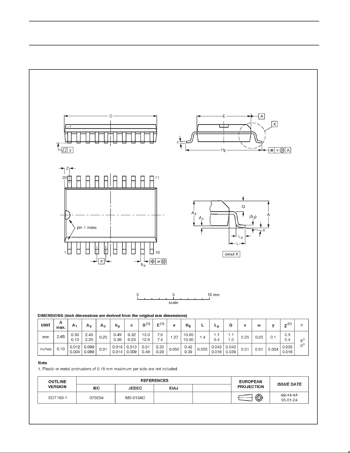
SO20: plastic small outline package; 20 leads; body width 7.5 mm SOT163-1
1997 Nov 07
12
Page 13
Philips Semiconductors Product specification
SA575Low voltage compandor
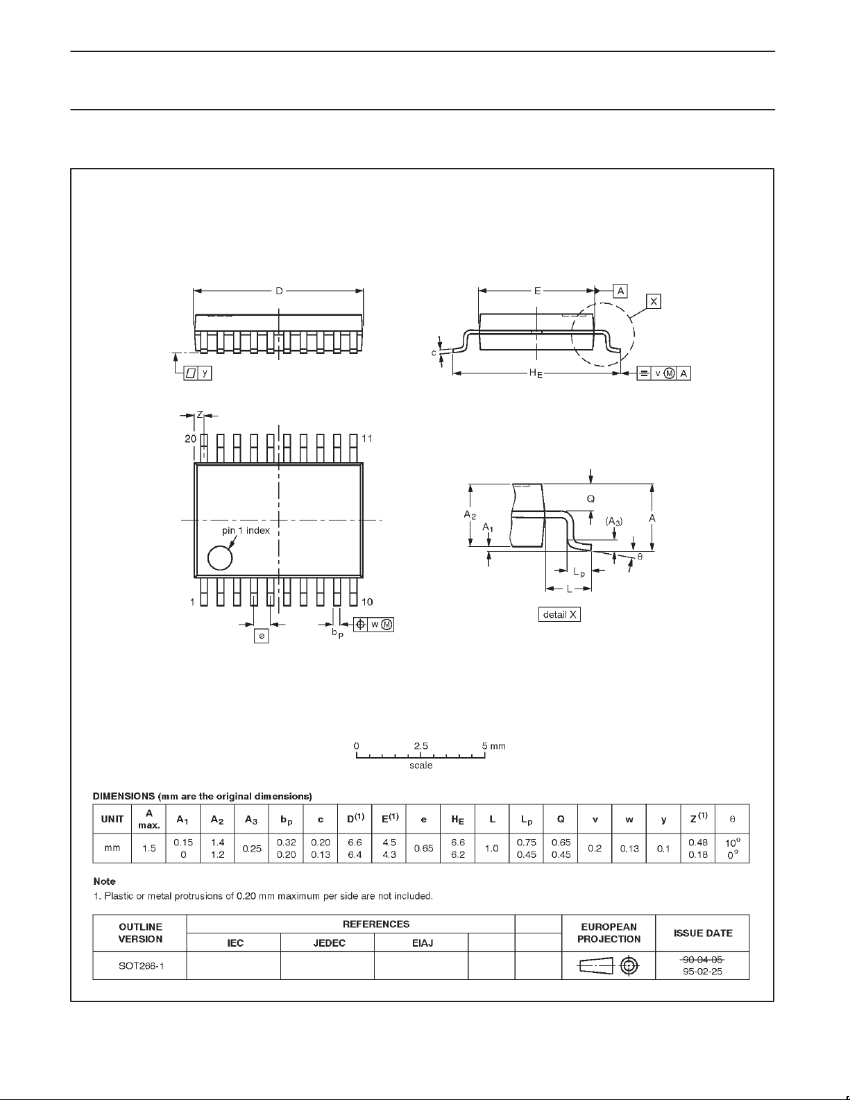
SSOP20: plastic shrink small outline package; 20 leads; body width 4.4 mm SOT266-1
1997 Nov 07
13
Page 14

Philips Semiconductors Product specification
SA575Low voltage compandor
DEFINITIONS
Data Sheet Identification Product Status Definition
Objective Specification
Preliminary Specification
Product Specification
Formative or in Design
Preproduction Product
Full Production
Philips Semiconductors and Philips Electronics North America Corporation reserve the right to make changes, without notice, in the products,
including circuits, standard cells, and/or software, described or contained herein in order to improve design and/or performance. Philips
Semiconductors assumes no responsibility or liability for the use of any of these products, conveys no license or title under any patent, copyright,
or mask work right to these products, and makes no representations or warranties that these products are free from patent, copyright, or mask
work right infringement, unless otherwise specified. Applications that are described herein for any of these products are for illustrative purposes
only. Philips Semiconductors makes no representation or warranty that such applications will be suitable for the specified use without further testing
or modification.
LIFE SUPPORT APPLICA TIONS
Philips Semiconductors and Philips Electronics North America Corporation Products are not designed for use in life support appliances, devices,
or systems where malfunction of a Philips Semiconductors and Philips Electronics North America Corporation Product can reasonably be expected
to result in a personal injury. Philips Semiconductors and Philips Electronics North America Corporation customers using or selling Philips
Semiconductors and Philips Electronics North America Corporation Products for use in such applications do so at their own risk and agree to fully
indemnify Philips Semiconductors and Philips Electronics North America Corporation for any damages resulting from such improper use or sale.
Philips Semiconductors
811 East Arques Avenue
P.O. Box 3409
Sunnyvale, California 94088–3409
Telephone 800-234-7381
This data sheet contains the design target or goal specifications for product development. Specifications
may change in any manner without notice.
This data sheet contains preliminary data, and supplementary data will be published at a later date. Philips
Semiconductors reserves the right to make changes at any time without notice in order to improve design
and supply the best possible product.
This data sheet contains Final Specifications. Philips Semiconductors reserves the right to make changes
at any time without notice, in order to improve design and supply the best possible product.
Copyright Philips Electronics North America Corporation 1997
All rights reserved. Printed in U.S.A.
1997 Nov 07
14
 Loading...