

Datasheet NE555N, NE555, NE555D, SA555N, SA555 Datasheet (SGS Thomson Microelectronics)
...Page 1
NE555
GENERALPURPOSE SINGLE BIPOLAR TIMERS
.LOW TURN OFF TIME
.MAXIMUM OPERATING FREQUENCY
GREATERTHAN500kHz
.TIMINGFROMMICROSECONDSTO HOURS
.OPERATES IN BOTH ASTABLE AND
MONOSTABLEMODES
.HIGHOUTPUT CURRENT CAN SOURCE OR
SINK200mA
.ADJUSTABLE DUTYCYCLE
.TTL COMPATIBLE
.TEMPERATURE STABILITY OF 0.005%
DESC RIP TI ON
TheNE555monolithictimingcircuitisahighlystable
controllercapableofproducingaccuratetimedelays
or oscillation.In the time delay modeof operation,
the time is precisely controlledby one externalresistorandcapacitor.Forastableoperationasanoscillator,thefree runningfrequency andthe duty cycle are both accuratelycontrolledwithtwoexternal
resistorsandone capacitor.The circuit maybe triggered and reseton fallingwaveforms, andthe output structurecan source or sinkup to 200mA. The
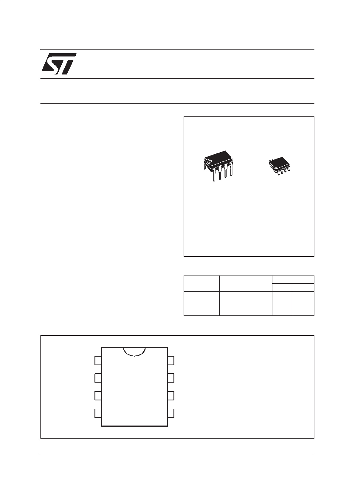
NE555 is available in plastic and ceramic minidip
packageandina8-leadmicropackageandinmetal
can packageversion.
PER
o
C
N
DIP8
(PlasticPackage)
ORDER CODES
Part
Number
NE555 0
SA555 –40
SE555 –55
Temperature
SA555 - SE555
D
SO8
(PlasticMicropackage)
Package
Range
o
C, 70oC ••
o
C, 105oC ••
o
C, 125oC ••
ND
PIN CONNE CTIONS (top view)
1
2
3
45
July 1998
8
7
6
1 - GND
2 - Trigger
3 - Output
4 - Reset
5 - Control voltage
6 - Threshold
7 - Discharge
8-V
CC
1/10
Page 2
NE 555/SA555/SE555
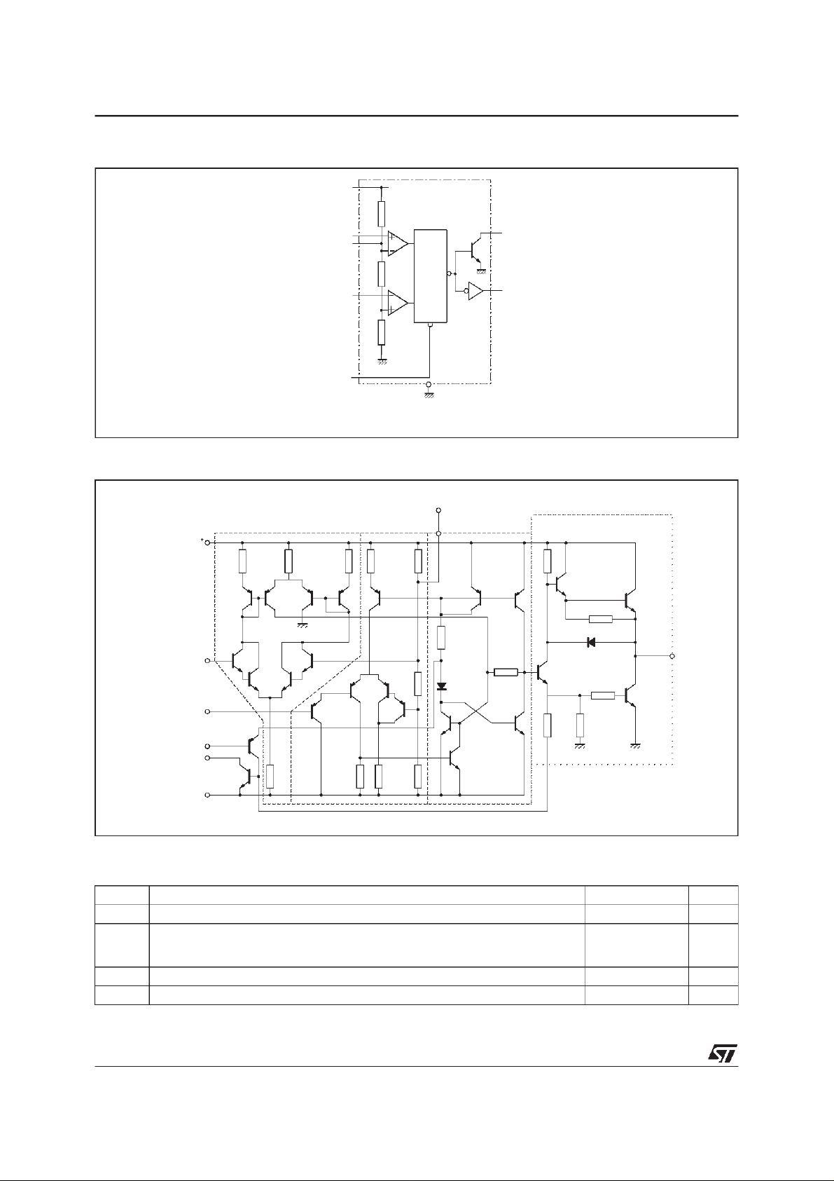
BLOCK DI AGRAM
THRESHOLD
CONTROL VOLTAGE
TRIGGER
+
V
CC
5kΩ
COMP
5kΩ
COMP
5kΩ
R
FLIP-FLOP
S
INHIBIT/
RESET
Q
DISCHARGE
OUT
SCHE MATIC DIAGRAM
THRESHOLD
COMPARATOR
V
CC
Q5 Q6 Q7 Q8 Q9
THRESHOLD
TRIGGER
RESET
DISCHARGE
GND
Q1
2
4
7
Q14
1
4.7k
R1
Q2
Q15
RESET
S -8086
R2
R3
830Ω
Ω
Q3
R5
10kΩ
4.7k
Q4
Q10
100kΩ
Ω
R6
Q11 Q12
1k
R4
Ω
Q13
R7
100kΩ
S
CONTROL
VOLTAGE
5
R8
5k
Ω
R9
5kΩ
Q16 Q18
R10
5kΩ
R11
5kΩ
D2
Q17
Q19
R17
4.7k
Ω
R12
6.8kΩ
Q20
Q23
R16
100Ω
Q21
3.9kΩ
D1
R15
4.7k
OUTPUT
Ρ13
R14
220
Ω
Ω
Q22
3
Q24
TRIGGER COMPARATOR F LIP FLOP
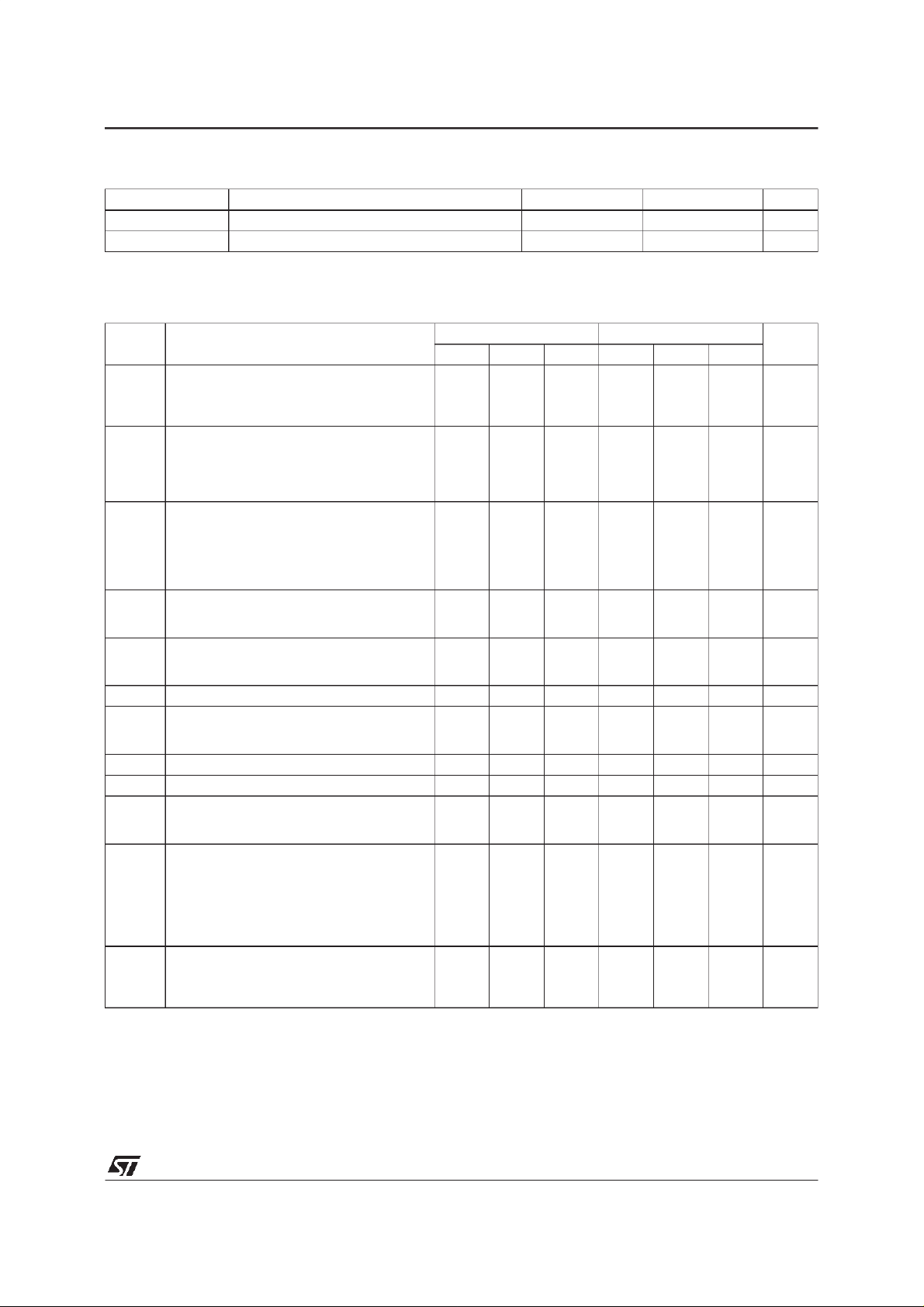
ABSOLUTE MAXIMUM RATINGS
Symbol Parameter Value Unit
V
T
T
2/10
Supply Voltage 18 V
cc
Operating Free Air Temperature Range for NE555
oper
for SA555
for SE555
T
Junction Temperature 150
j
Storage Temperature Range –65 to 150
stg
0to70
–40 to 105
–55 to 125
o
C
o
C
o
C
Page 3
NE 555/SA 555/S E 555
OPERATINGCONDITIONS
Symbol Parameter SE555 NE555 - SA555 Unit
V
CC
V
th,Vtrig,Vcl,Vreset
ELECTRICAL CHARACTERISTICS
= +25oC, VCC= +5V to +15V (unless otherwisespecified)
T
amb
Symbol Parameter
I
V
V
V
I
V
V
Notes : 1. Supply current whenoutput is high is typically1mA less.
Supply Current (RL∞) (- note 1)
CC
Low State V
High State V
Timing Error (monostable)
(R
A=
Initial Accuracy - (note 2)
Drift with Temperature
Drift with Supply Voltage
Timing Error (astable)
(R
A,RB
V
CC
Initial Accuracy - (note 2)
Drift with Temperature
Drift with Supply Voltage
Control Voltage level
CL
Threshold Voltage
V
th
Threshold Current - (note 3) 0.1 0.25 0.1 0.25 µA
I
th
Trigger Voltage
trig
Trigger Current (V
I
trig
Reset Voltage - (note 4) 0.4 0.7 1 0.4 0.7 1 V
reset
Reset Current
reset
Low Level Output Voltage
OL
V
CC
V
CC
High Level Output Voltage
OH
V
CC
V
CC
2. Tested at V
3. This willdetermine the maximum value of R
the max total R = 3.5MΩ.
Supply Voltage 4.5 to 18 4.5 to 18 V
Maximum Input Voltage V
CC
V
CC
SE555 NE555 - SA555
Min. Typ. Max. Min. Typ. Max.
V
CC
CC
CC
=+5V
= +15V
=5V
10
3
2
12
5
3
10
2
2k to 100kΩ, C = 0.1µF)
0.5
30
0.05
2
100
0.2
1
50
0.1
=1kΩto 100kΩ, C = 0.1µF,
= +15V)
= +15V, I
= +5V, I
= +15V, I
= +5V, I
= +5V and VCC= +15V.
CC
1.5
90
0.15
= +15V
V
CC
=+5V
V
CC
= +15V
V
CC
=+5V
V
CC
= +15V
V
CC
=+5V
V
CC
= 0V) 0.5 0.9 0.5 2.0 µA
trig
= +0.4V
V
reset
=0V
V
reset
= 10mA
O(sink)
= 50mA
I
O(sink)
= 100mA
I
O(sink)
= 200mA
I
O(sink)
= 8mA
O(sink)
= 5mA
I
O(sink)
O(source)
I
O(source)
O(source)
= 200mA
= 100mA
= 100mA
A+RB
9.6
2.9
9.4
2.7
4.8
1.4551.67
13
3
for +15V operation themax total is R = 20MΩ and for 5V operation
10
3.33
10
3.33
0.1
0.4
0.1
0.4
2
2.5
0.1
0.05
12.5
13.3
3.3
10.4
3.8
10.6
4
5.2
1.9
0.4
1
0.15
0.5
2.2
0.25
0.2
2.6
8.8
2.4
4.5
1.1
12.75
2.75
2.25
150
0.3
9
10
3.33
10
3.33
5
1.67
0.1
0.4
0.1
0.4
2
2.5
0.3
0.25
12.5
13.3
3.3
6
15
3
0.5
11
4
11.2
4.2
5.6
2.2
0.4
1.5
0.25
0.75
2.5
0.4
0.35
V
Unit
mA
%
ppm/°C
%/V
%
ppm/°C
%/V
V
V
V
mA
V
V
3/10
Page 4

NE 555/SA555/SE555
ELECTRICAL CHARACTERISTICS (continued)
Symbol Parameter
I
dis(off)
V
dis(sat)
Notes : 5. No protection against excessive Pin 7 current isnecessary, providing the package dissipation rating will notbe exceeded.
Discharge Pin Leakage Current
(output high) (V
dis
= 10V)
Discharge pin Saturation Voltage
(output low) - (note 5)
= +15V, I
V
CC
= +5V, I
V
CC
Output Rise Time
t
r
t
Output Fall Time
f
t
Turn off Time - (note 6) (V
off
6. Timemesaured from a positive going input pulse from 0 to 0.8x V
output trigger istied to treshold.
dis
= 4.5mA
dis
= 15mA
reset=VCC
) 0.5 0.5 µs
Min. Typ. Max. Min. Typ. Max.
SE555 NE555 - SA555
20 100 20 100 nA
180
80
100
100
CC
480
200
200
200
into the threshold to the drop from high to low of the
180
80
100
100
480
200
300
300
Unit
mV
ns
Figure1 : Minimum PulseWidth Requiredfor
Figure 2 : SupplyCurrent versusSupplyVoltage
Trigering
Figure 3 : DelayTime versusTemperature Figure4 : Low OutputVoltageversus Output
SinkCurrent
4/10
Page 5

NE 555/SA 555/S E 555
Figure 5 : Low OutputVoltageversusOutput
SinkCurrent
Figure 7 : HighOutput VoltageDrop versus
Output
Figure 6 : LowOutput VoltageversusOutput
SinkCurrent
Figure 8 : DelayTime versusSupplyVoltage
Figure9 : PropagationDelay versusVoltage
Level of Trigger Value
5/10
Page 6

NE 555/SA555/SE555
APPLICATION INFORMATI ON
MONOSTABLEOPERATION
In the monostable mode, the timer functions as a
one-shot.Referring tofigure10 theexternalcapacitor is initially held dischargedby a transistorinside
thetimer.
Figure10
V
= 5 to 15V
CC
Reset
R1
Trigger
Output
4
2
3
NE555
1
8
7
6
Control Voltage
5
0.01
C1
µF
Thecircuit triggerson a negative-goinginput signal
whenthelevelreaches1/3Vcc.Oncetriggered,the
circuit remains in this state until the set time has
elapsed,even if it is triggeredagain duringthis interval.ThedurationoftheoutputHIGHstateisgiven
by t = 1.1 R
andis easily determinedby
1C1
figure12.
Notice that since the chargerate and the threshold
levelofthecomparatorarebothdirectlyproportional
tosupply voltage,thetimingintervalis independent
ofsupply.Applyinga negativepulsesimultaneously
tothe resetterminal(pin 4) and the triggerterminal
(pin2) duringthe timingcycle dischargesthe externalcapacitorandcausesthecycletostartover.The
timingcycle now startson thepositiveedgeof the
resetpulse. During the time the reset pulse in applied,the output is drivento itsLOW state.
Whenanegativetriggerpulseisappliedtopin2,the
flip-flop isset, releasingthe short circuitacross the
externalcapacitoranddriving theoutputHIGH.The
voltage across the capacitor increases exponentiallywith thetimeconstantτ =R
ageacrossthecapacitorequals2/3V
. Whenthe volt-
1C1
,thecompa-
cc
ratorresetstheflip-flopwhichthendischargethecapacitor rapidly and drivers the output to its LOW
state.
Figure 11showstheactualwaveformsgeneratedin
thismode of operation.
When Reset is not used, it should be tied high to
avoidany possiblyor false triggering.
Figure 11
t = 0.1 ms / div
INPUT = 2.0V/div
OUTPUT VOLTAGE = 5.0V/div
CAPACITOR VOLTAGE = 2.0V/div
R1 = 9.1kΩ, C1 = 0.01µF, R = 1kΩ
L
Figure 12
C
(µF)
10
1.0
0.1
0.01
0.001
10 100 1.0 10 100 10 (t )
µs µs
Ω
R1= 1k
10kΩ
10
Ω
k
0
1MΩ
10M
ms ms ms s
Ω
d
ASTABLEOPERATION
Whenthe circuitis connectedasshownin figure13
(pin2and6connected)ittriggersitselfandfreeruns
as a multivibrator. The external capacitor charges
throughR
andR2and discharges throughR2only.
1
Thusthedutycyclemay bepreciselysetbythe ratio
of thesetworesistors.
In the astablemode of operation,C
dischargesbetween 1/3 V
and 2/3 Vcc. Asin the
cc
chargesand
1
triggeredmode,thechargeanddischargetimesand
thereforefrequencyare independentof the supply
voltage.
6/10
Page 7

NE 555/SA 555/S E 555
Figure 13
VCC= 5 to 15V
R1
R2
C1
0.01
Output
µF
Control
Voltage
48
3
NE555
5
1
7
6
2
Figure14showsactualwaveformsgeneratedinthis
modeof operation.
Thecharge time(outputHIGH)is givenby :
t
=0.693 (R1+R2)C
1
1
andthe dischargetime (outputLOW) by :
=0.693 (R2)C
t
2
1
Thusthe total periodT isgivenby :
T=t
=0.693(R1+2R2)C
1+t2
1
Thefrequencyofoscillationis them :
f =
1
T
=
(R
1
1.44
+ 2R2) C
1
andmay beeasily foundby figure 15.
Theduty cycleis givenby :
R
D =
2
R1+ 2R
2
Figure 14
t = 0.5 ms / div
OUTPUT VOLTAGE= 5.0V/div
Figure 15 : Free RunningFrequencyversusR1,
andC
R
2
C
(µF)
10
1.0
0.1
0.01
0.001
R
1
+
0.1 1 10 100 1k 10k f (Hz)
1
1
k
Ω
1
0
k
Ω
1
0
0
k
1
Ω
M
R
Ω
2
=
1
0M
Ω
o
PULSEWIDTHMODULATOR
When the timer is connected in the monostable
mode and triggered with a continuouspulse train,
theoutputpulsewidthcanbemodulatedbyasignal
appliedto pin 5. Figure16 shows the circuit.
Figure 16 : Pulse Width Modulator.
V
CC
R
A
8
7
6
Modulation
Input
5
1
C
Trigger
Output
4
2
NE555
3
CAPACITOR VOLTAGE = 1.0V/div
R1 = R2 = 4.8kΩ, C1= 0.1µF, R = 1kΩ
L
7/10
Page 8

NE 555/SA555/SE555
LINEARRAMP
Whenthe pullupresistor,R
, in themonostablecir-
A
cuitisreplacedbyaconstantcurrentsource,alinear
ramp is generated.Figure 17 shows a circuit configuration that will performthis function.
Figure17.
V
CC
R
E
R1
C
R2
Trigger
Output
NE555
1
8
7
2N4250
or equiv.
6
5
0.01µF
4
2
3
Figure 18showswaveformsgeneratorbythelinear
ramp.
Thetime intervalis given by :
T =
(2/3V
R
1VCC
RE(R
CC
1+
− VBE(R1+R
R
2)
C
VBE= 0.6V
2)
50%DUTY CYCLE OSCILLATOR
Fora 50% duty cycle the resistorsR
andREmay
A
beconnectedasin figure19.Thetimepreriodforthe
outputhigh is the sameas previous,
=0.693RAC.
t
1
For theoutputlow it ist
[(R
)⁄ (RA+ RB)] CLn
ARB
Thusthefrequencyof oscillationis f
=
2
2RB− R
RB− 2R
A
A
1
=
t
+ t
1
2
Notethat thiscircuit will not oscillateifRBisgreater
Figure 19 : 50%DutyCycleOscillator.
V
Out
CC
4
2
3
NE55
1
8
R
7
6
5
B
22kΩ
0.01µF
V
R
A
51kΩ
C
0.01µF
CC
Figure 18 : LinearRamp.
VCC= 5V Top trace : input 3V/DIV
Time = 20µs/DIV Middle trace : output 5V/DIV
= 47kΩ Bottom trace : output 5V/DIV
R
1
= 100kΩ Bottom trace : capacitor voltage
R
2
= 2.7kΩ 1V/DIV
R
E
C = 0.01µF
than1/2 R
notbringpin2 downto1/3V
becausethejunctionofRAand RBcan-
A
andtriggerthelower
CC
comparator.
ADDITIONALINFORMATION
Adequatepower supply bypassingis necessaryto
protect associated circuitry. Minimum recommendedis 0.1µF in parallel with 1µF electrolytic.
8/10
Page 9

PACKAG E MECHANI CAL DATA
8 PINS - PLASTIC DIP
NE 555/SA 555/S E 555
Dimensions
Min. Typ. Max. Min. Typ. Max.
Millimeters Inches
A 3.32 0.131
a1 0.51 0.020
B 1.15 1.65 0.045 0.065
b 0.356 0.55 0.014 0.022
b1 0.204 0.304 0.008 0.012
D 10.92 0.430
E 7.95 9.75 0.313 0.384
e 2.54 0.100
e3 7.62 0.300
e4 7.62 0.300
F 6.6 0260
i 5.08 0.200
L 3.18 3.81 0.125 0.150
Z 1.52 0.060
PM-DIP8.EPS
DIP8.TBL
9/10
Page 10

NE 555/SA555/SE555
PACKAG E MECHANI CAL DATA
8 PINS - P LASTIC MICROPACKAGE (SO)
Dimensions
Min. Typ. Max. Min. Typ. Max.
Millimeters Inches
A 1.75 0.069
a1 0.1 0.25 0.004 0.010
a2 1.65 0.065
a3 0.65 0.85 0.026 0.033
b 0.35 0.48 0.014 0.019
b1 0.19 0.25 0.007 0.010
C 0.25 0.5 0.010 0.020
c1 45
o
(typ.)
D 4.8 5.0 0.189 0.197
E 5.8 6.2 0.228 0.244
e 1.27 0.050
e3 3.81 0.150
F 3.8 4.0 0.150 0.157
L 0.4 1.27 0.016 0.050
M 0.6 0.024
S8
Information furnished is believed to be accurate and reliable. However, STMicroelectronics assumes no responsibility for the
consequences of use of such information nor for any infringement of patents or other rights of third parties which may result
from its use. No license is granted by implication or otherwise under any patent or patent rights of STMicroelectronics. Specifications mentioned in this publication are subject to change without notice. This publication supersedes and replaces all information previously supplied. STMicroelectronics products are not authorized for use as critical components in life support
devices or systems without express written approval of STMicroelectronics.
The ST logois a trademark of STMicroelectronics
o
(max.)
PM-SO8.EPS
SO8.TBL
1998 STMicroelectronics – Printed in Italy – All Rights Reserved
STMicroelectronics GROUP OF COMPANIES
Australia - Brazil- Canada - China - France - Germany - Italy - Japan - Korea - Malaysia - Malta - Mexico - Morocco
The Netherlands - Singapore - Spain - Sweden - Switzerland- Taiwan - Thailand - United Kingdo m- U.S.A.
10/10
ORDERCODE :
 Loading...