

Page 1
Philips Semiconductors Product specification
SA5222Low-power FDDI transimpedance amplifier
1
1995 Apr 26 853-1582 15170
DESCRIPTION
The NE/SA5222 is a low-power, wide-band, low noise
transimpedance amplifier with differential outputs, optimized for
signal recovery in FDDI fiber optic receivers. The part is also suited
for many other RF and fiber optic applications as a general purpose
gain block.
FEATURES
•Extremely low noise:
z
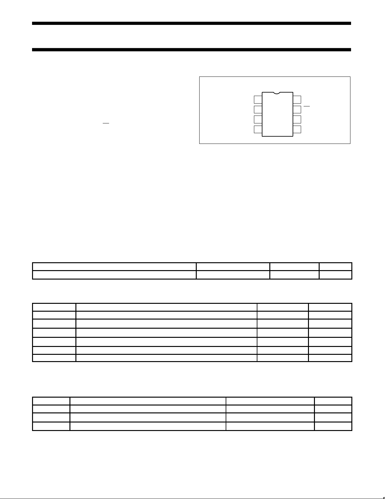
D Package
IN
GND
2
OUT
V
CC2
1
2
3
4
8
7
6
5
OUT
GND
1
V
CC1
GND
1
SD00360
Figure 1. Pin Configuration
APPLICATIONS
•FDDI preamp
•Current-to-voltage converters
•Wide-band gain block
•Medical and scientific instrumentation
•Sensor preamplifiers
•Single-ended to differential conversion
•Low noise RF amplifiers
•RF signal processing
ORDERING INFORMATION
DESCRIPTION TEMPERATURE RANGE ORDER CODE DWG #
8-Pin Plastic Small Outline (SO) package
-40 to +85°C
SA5222D SOT96-1
ABSOLUTE MAXIMUM RATINGS
SYMBOL PARAMETER RATING UNITS
V
CC1,2
Power supply voltage 6 V
T
A
Ambient temperature range -40 to +85
°C
T
J
Junction temperature range -55 to +150
°C
T
STG
Storage temperature range -65 to +150
°C
P
D
Power dissipation TA = 25oC (still air)
1
0.78 W
I
INMAX
Maximum input current 5 mA
NOTE:
1. Maximum power dissipation is determined by the operating ambient temperature and the thermal resistance θJA = 158oC/W. Derate
6.2mW/
°C above 25°C.
RECOMMENDED OPERATING CONDITIONS
SYMBOL PARAMETER RATING UNITS
V
CC1,2
Power supply voltage 4.5 to 5.5 V
T
A
Ambient temperature range: SA grade -40 to +85
°C
T
J
Junction temperature range: SA grade -40 to +105
°C
2.0pAH
•Single 5V supply
•Low supply current: 9mA
•Large bandwidth: 165MHz
•Differential outputs
•Low output offset
•Low input/output impedances
•High power-supply-rejection ratio: 55dB
•Tight transresistance control
•High input overload: 115µA
•ESD protected
PIN DESCRIPTION
Page 2
Philips Semiconductors Product specification
SA5222Low-power FDDI transimpedance amplifier
1995 Apr 26
2
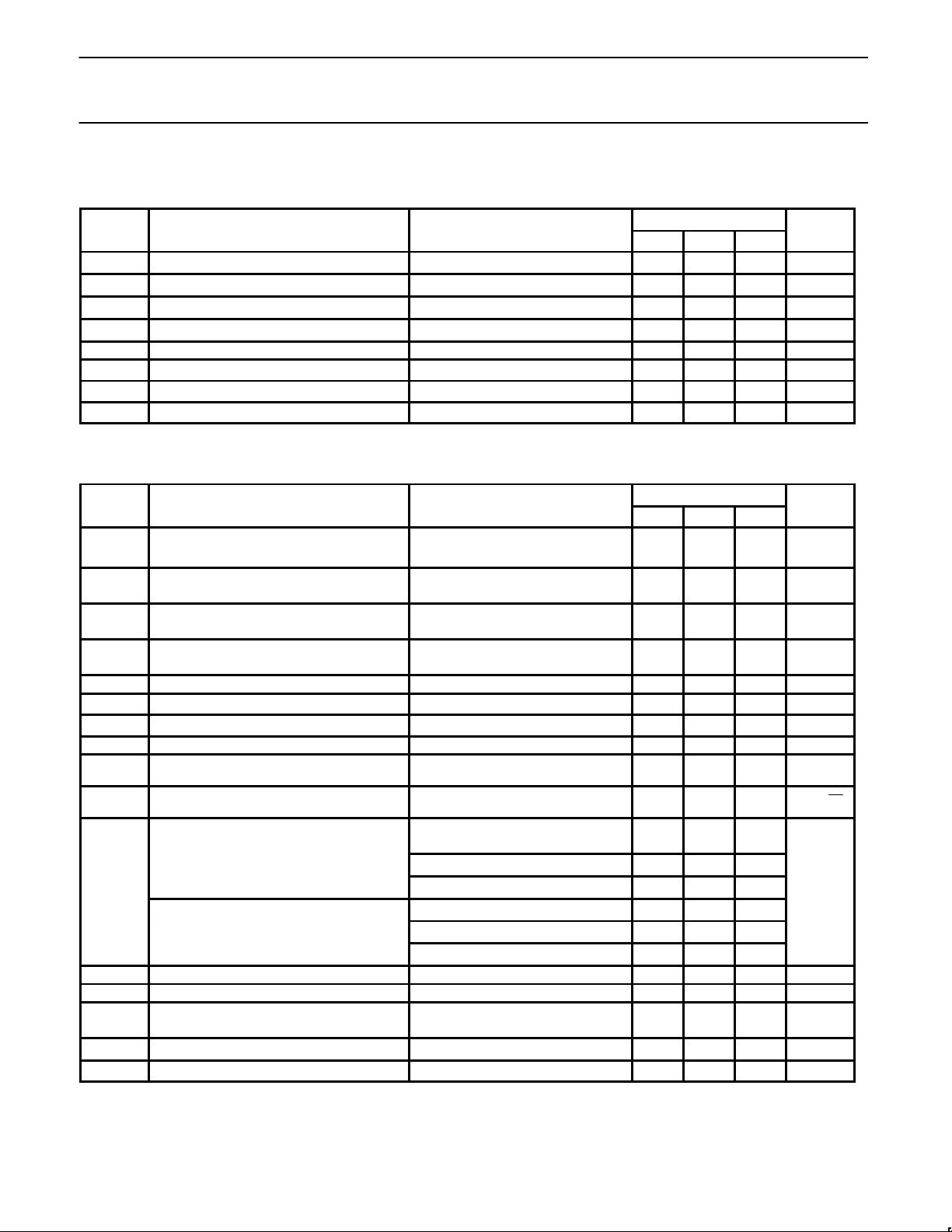
DC ELECTRICAL CHARACTERISTICS
Typical data and Min and Max limits apply at TA = 25°C, and V
CC1
= V
CC2
= +5V, unless otherwise specified.
SA5222
SYMBOL
PARAMETER
TEST CONDITIONS
Min Typ Max
UNIT
V
IN
Input bias voltage 1.3 1.55 1.8 V
V
O
±
Output bias voltage 2.9 3.2 3.5 V
V
OS
Output offset voltage 0 ±100 mV
I
CC
Supply current 6 9 12 mA
I
OMAX
Output sink/source current 1.5 2 mA
I
IN
Input current (2% linearity) Test circuit 5, Procedure 2 ±60 ±90
µA
I
INMAX
Maximum input current overload threshold Test circuit 5, Procedure 4 ±80 ±115
µA
V
OMAX
Maximum differential output voltage swing R
L
= ∞, Test Circuit 5, Procedure 3 3.6 V
P-P
AC ELECTRICAL CHARACTERISTICS
Typical data and Min and Max limits apply at TA = 25°C and V
CC1
= V
CC2
=+5V, unless otherwise specified.
SA5222
SYMBOL
PARAMETER
TEST CONDITIONS
Min Typ Max
UNIT
R
T
Transresistance (differential output)
DC tested, RL = ∞, Test Circuit 5,
Procedure 1
13.3 16.6 19.9 kΩ
R
O
Output resistance
(differential output)
DC tested 30 60 90 Ω
R
T
Transresistance
(single-ended output)
DC tested, RL = ∞
6.65 8.3 9.95 kΩ
R
O
Output resistance
(single-ended output)
DC tested 15 30 45 Ω
f
3dB
Bandwidth (-3dB)
1
Test Circuit 1 110 140 MHz
R
IN
Input resistance 150
Ω
C
IN
Input capacitance
2
1
pF
∆R/∆V Transresistance power supply sensitivity V
CC1
= V
CC2
= 5 ±0.5V 1.0 %/V
∆R/∆T
Transresistance ambient temperature sensitivity
∆TA = T
A MAX
- T
A MIN
0.07
%/oC
I
IN
RMS noise current spectral density (referred
to input)
Test Circuit 2, f = 10MHz 2.0
p
Integrated RMS noise current over the bandwidth (referred to input)
Test circuit 2,
∆f = 50MHz
15
CS = 0pF ∆f = 100MHz 25
∆f = 150MHz 36
I
T
CS = 1pF ∆f = 50MHz 17
nA
∆f = 100MHz 35
∆f = 150MHz 55
PSRR Power supply rejection ratio DC Tested, ∆VCC = ±0.5V –55 dB
PSRR Power supply rejection ratio
3
f = 1.0MHz, Test Circuit 3 –34 dB
I
INMAX
Maximum input amplitude for output duty
cycle of 50 ±5%
4
Test circuit 4 ±120 µA
tr, tfRise and fall times 10 – 90% 2.2 ns
t
D
Group delay f = 10MHz 2.2 ns
NOTES:
1. Bandwidth is tested into 50Ω load. Bandwidth into 1kΩ load is approximately 165MHz.
2. Does not include Miller-multiplied capacitance of input device.
3. PSRR is output referenced and is circuit board layout dependent at higher frequencies. For best performance use a RF filter in V
CC
line.
4. Monitored in production via linearity and over load tests.
I
T
A Hz
nA
Page 3
Philips Semiconductors Product specification
SA5222Low-power FDDI transimpedance amplifier
1995 Apr 26
3
TEST CIRCUITS
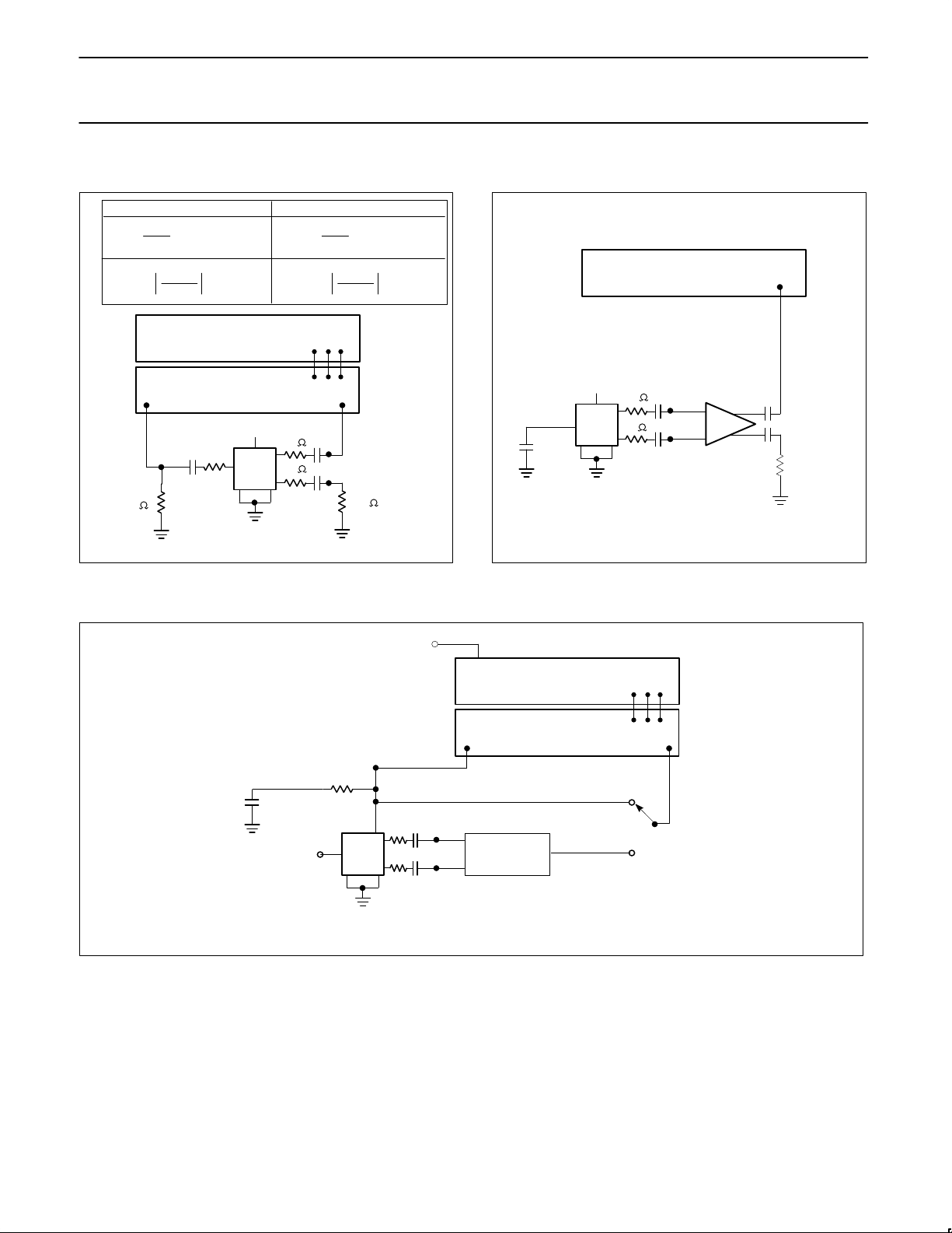
Test Circuit 1: Bandwidth
NETWORK ANALYZER
S-PARAMETER TEST SET
PORT1 PORT2
V
CC
20
.1uF
20
.1uF
50
Z
O
= 50Ω
OUT
OUT
IN DUT
0.1uF
R=1k
50
GND
1
SINGLE-ENDED
DIFFERENTIAL
RO = Z
O
1 + S22
1 - S22
-20
RO = 2Z
O
1 + S22
1 - S22
-40
GND
2
RT+
V
OUT
V
IN
R + 4 @ S21@ RRT+
V
OUT
V
IN
R + 2 @ S21@ R
Z
O
= 50Ω
SD00361
Figure 2. Test Circuit1
Test Circuit 2: Noise
SPECTRUM ANALYZER
V
CC
20
20
OUT
OUT
IN DUT
GND
2
GND
1
NE5209
50Ω
.1µF
.1µF
10µF
10µF
C
S
50Ω
SD00362
Figure 3. Test Circuit2
TEST CIRCUITS (continued)
Test Circuit 3: PSRR
NETWORK ANALYZER
S-PARAMETER TEST SET
PORT1 PORT2
V
CC
20Ω
.1uF
20Ω
.1uF
OUT
OUT
IN DUT
GND
2
GND
1
50Ω
CAL
UNBAL.
0.1uF
NC
50Ω
BIAS TEE
5V
NHO300HB
TRANSFORMER
CONVERSION
LOSS = 9dB
100Ω
BAL.
SD00363
Figure 4. Test Circuit4
Page 4
Philips Semiconductors Product specification
SA5222Low-power FDDI transimpedance amplifier
1995 Apr 26
4
TEST CIRCUITS (continued)
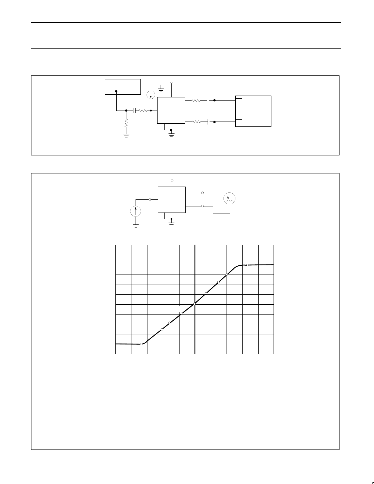
Test Circuit 4: Duty Cycle Distortion
PULSE GEN
OUT
OUT
DUT
OSCILLOSCOPE
A
B
Meaurement done using
differential wave forms
5V
0.1uF
.1µF
.1µF
GND
1
GND
2
ZO = 50Ω
Z
O
= 50Ω
IN
1kΩ
1kΩ
1kΩ
50Ω
OFFSET
SD00364
Figure 5. Test Circuit4
TEST CIRCUITS (continued)
Test Circuit 5: DC Tests
Typical V
O
(Differential) vs I
IN
SA5222 TEST CONDITIONS
Procedure 1
R
T
measured at 30µA
R
T
= (VO1 - VO2) / (+30µA - (-30µA)
Where: V
O1
Measure at IIN = +30µA
V
O2
Measured at IIN = -30µA
2.25
1.80
1.35
0.90
0.45
0.00
–0.45
–0.90
–1.35
–1.80
–2.25
–200 –160 –120 –80 –40 0 40 80 120 160 200
V
O8
V
O6
V
O4
V
O2
V
O1
V
O
3
V
O
5
V
O
7
V
O
S
CURRENT INPUT (µA)
DIFFERENTIAL OUTPUT VOLTAGE (V)
OUT +
OUT –
5V
I
IN (µA)
VO (VOLTS)
+
–
GND
1
GND
2
Procedure 2
Procedure 3 Procedure 4
Linearity = 1 - ABS((V
OA
- VOB / (VO3 - VO4))
Where: V
O3
Measured at IIN = +60µA
V
O4
Measured at IIN = -60µA
V
OA
= RT x (+60µA) + V
OS
VOB = RT x (-60µA) + V
OS
V
OMAX
= VO7 - V
O8
Where: VO7 Measured at IIN = +130µA
VO8 Measured at IIN = -130µA
I
INMAX
Test Pass Conditions:
V
O7
- VO5 > 50mV and VO6 - VO8 < 50mV
Where: VO5 Measured at IIN = +80µA
V
O6
Measured at IIN = -80µA
V
O7
Measured at IIN = +130µA
V
OB
Measured at IIN = -130µA
SD00365
Figure 6. Test Circuit5
Page 5
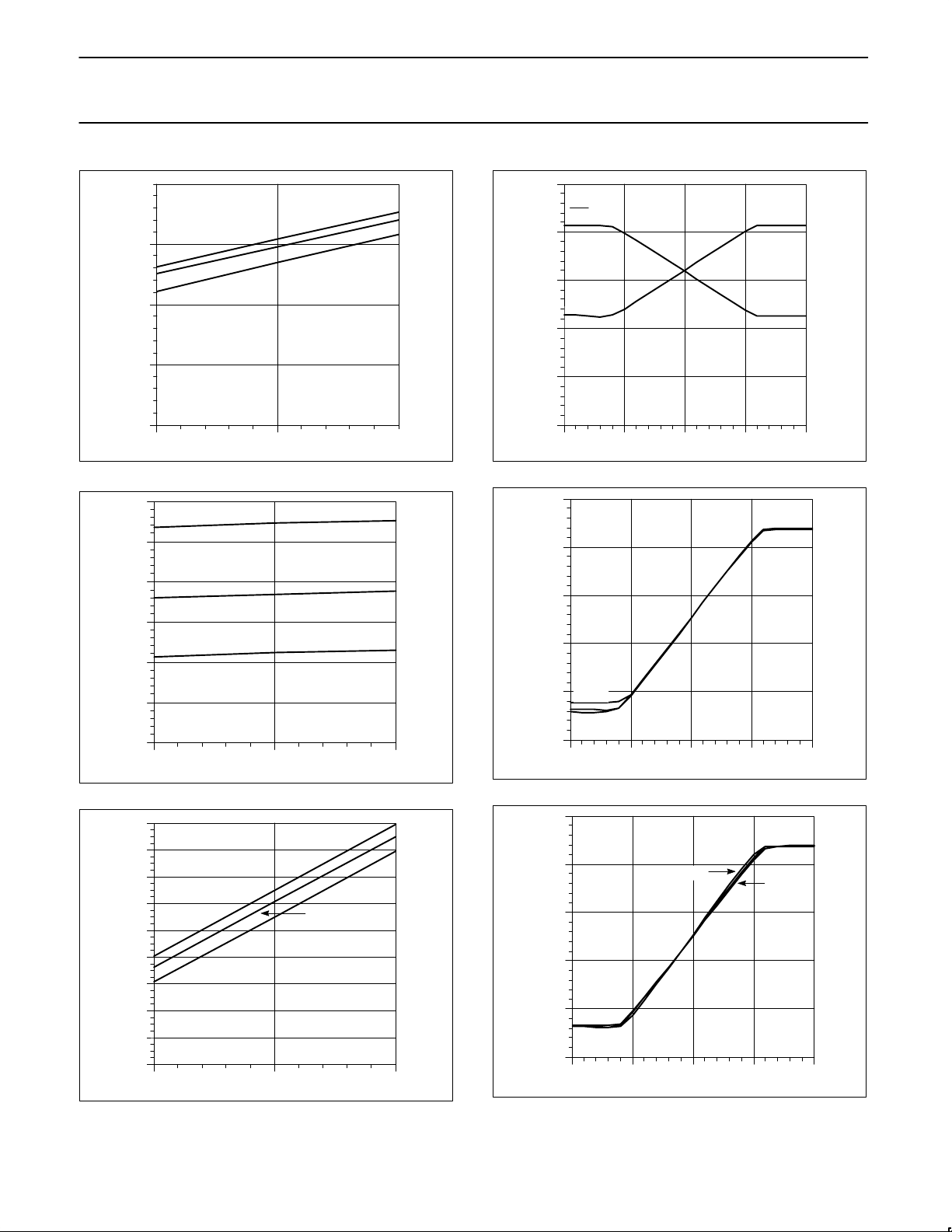
Philips Semiconductors Product specification
SA5222Low-power FDDI transimpedance amplifier
1995 Apr 26
5
6
7
8
9
10
4.5 5 5.5
SUPPLY VOLTAGE (V)
25°C
85°C
–40°C
SUPPLY CURRENT (mA)
SD00366
Figure 7. ICC vs. VCC and Temperature
1.2
1.3
1.4
1.5
1.6
1.7
1.8
4.5 5 5.5
SUPPLY VOLTAGE (V)
INPUT VOLTAGE (V)
25°C
85°C
–40°C
SD00546
Figure 8. Input Voltage vs. VCC and Temperature
2
2.2
2.4
2.6
2.8
3
3.2
3.4
3.6
3.8
4.5 5 5.5
SUPPLY VOLTAGE (V)
OUTPUT VOLTAGE (V)
PIN 6 OUTPUT
25°C
85°C
–40°C
SD00547
Figure 9. Output Voltage vs. VCC and Temperature
0
1
2
3
4
5
–200 –100 0 100 200
INPUT CURRENT (µA)
T
A
= +25°C
V
CC
= 5V
OUT
OUT
VOLTAGE (V)
SD00548
Figure 10. Differential Output Voltages vs. Input Current
–2.5
–1.5
–0.5
0.5
1.5
2.5
–200 –100 0 100 200
4.5V
5.5V
T
A
= +25°C
VOLTAGE (V)
INPUT CURRENT (µA)
SD00549
Figure 11. Differential Output Voltage vs Input Current and V
CC
–2.5
–1.5
–0.5
0.5
1.5
2.5
–200 –100 0 100 200
INPUT CURRENT (µA)
85°C
–40°C
V
CC
= 5V
VOLTAGE (V)
SD00550
Figure 12. Diff. Output Voltage vs. Input Current and Temp.
Page 6
Philips Semiconductors Product specification
SA5222Low-power FDDI transimpedance amplifier
1995 Apr 26
6
12
13
14
15
16
17
18
4.5 5 5.5
SUPPLY VOLTAGE (V)
25°C
85°C
–40°C
∆Iin = ±20µA
TRANSRESISTANCE (KOHMS)
SD00367
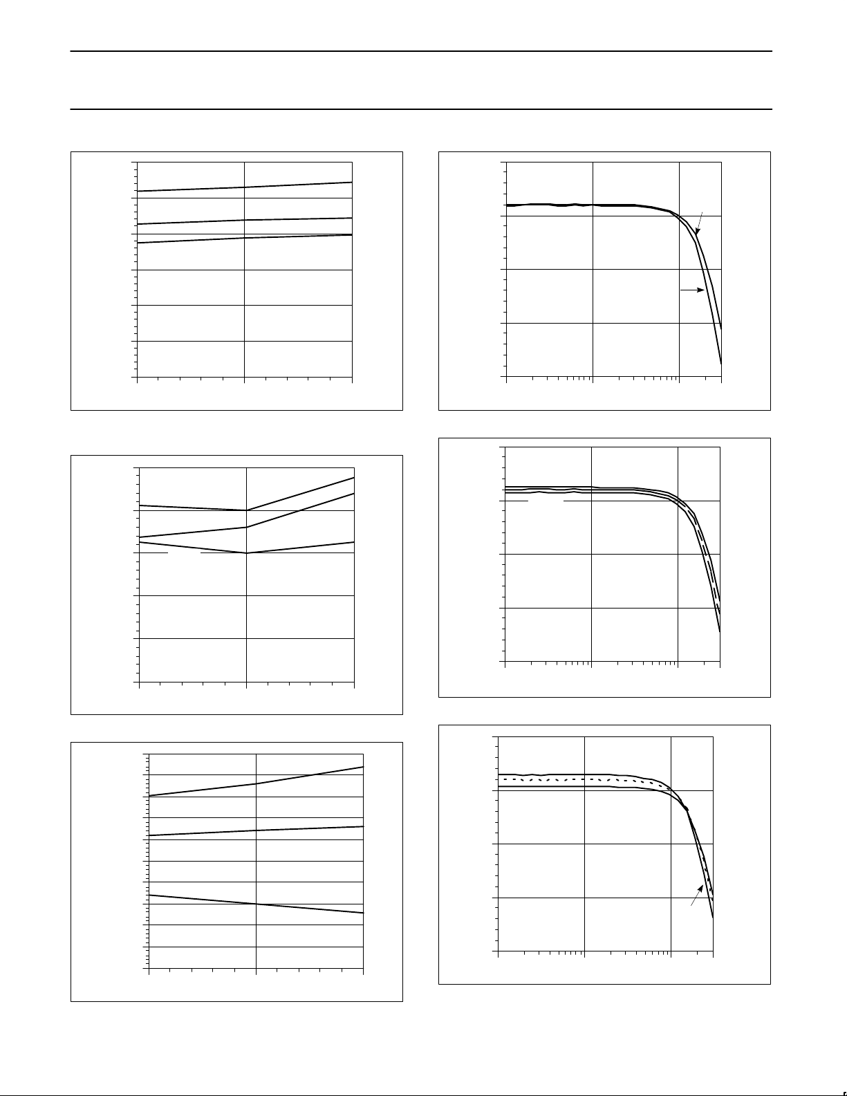
Figure 13. Differential Transresistance vs. VCC and
Temperature
10
20
30
40
50
4.5 5 5.5
SUPPLY VOLTAGE (V)
OUTPUT RESISTANCE (OHMS)
–40°C
85°C
25°C
0
SD00551
Figure 14. Output Resistance vs. VCC and Temperature
0
5
10
15
20
25
30
35
40
45
50
4.5 5 5.5
SUPPLY VOLTAGE (V)
25°C
85°C
–40°C
OUTPUT OFFSET (mV)
SD00552
Figure 15. Output Offset Voltage vs. VCC and Temperature
–5
0
5
10
15
1 10 100 300
FREQUENCY (MHz)
V
CC
= 5V
T
A
= +25°C
PIN 6
PIN 7
S (dB)
21
SD00553
Figure 16. Insertion Gain vs. Frequency
–5
0
5
10
15
1 10 100 300
FREQUENCY (MHz)
TA = +25°C
PIN 6 OUTPUT
5.5V
4.5V
S (dB)
21
SD00554
Figure 17. Insertion Gain vs. Frequency and V
CC
–5
0
5
10
15
1 10 100 300
FREQUENCY (MHz)
V
CC
= 5V
PIN 6 OUTPUT
–40°C
+85°C
+85°C
S (dB)
21
SD00555
Figure 18. Insertion Gain vs. Frequency and Temperature
Page 7
Philips Semiconductors Product specification
SA5222Low-power FDDI transimpedance amplifier
1995 Apr 26
7
–200
–100
0
100
200
1 10 100 300
FREQUENCY (MHz)
V
CC
= 5V
T
A
= +25°C
PIN 6 OUTPUT
PIN 7 OUTPUT
S PHASE (DEG)
21
SD00368
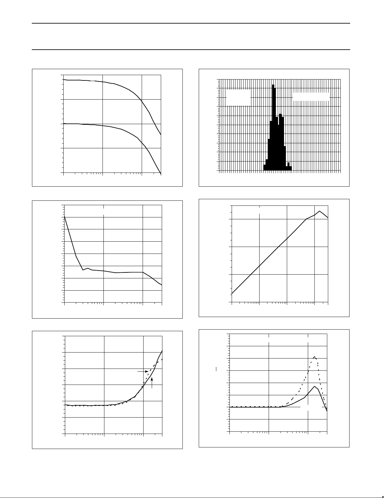
Figure 19. Phase vs. Frequency
0
1
2
3
4
5
6
7
8
1 10 100 300
FREQUENCY (MHz)
V
CC
= 5V
T
A
= +25°C
PIN 6 OUTPUT
0.1µF COUPLING CAP’s
S GROUP DELAY (ns)
21
SD00556
Figure 20. Group Delay vs. Frequency
–5
15
35
55
75
95
115
1 10 100 300
FREQUENCY (MHz)
V
CC
= 5V
T
A
= +25°C
PIN 6
PIN 7
Z MAGNITUDE (OHMS)
OUT
SD00557
Figure 21. Output Impedance vs. Frequency
0
5
10
15
20
25
30
35
40
45
50
110
170
140
FREQUENCY
VCC = 5V
50
Ω
Load
TA = 25°C
300 PARTS FROM
3 WAFERS
BANDWIDTH (MHz)
SD00558
Figure 22. –3dB Bandwidth Distribution
VCC = 5V
T
A
= +25°C
PSRR (dB)
–60
–4
0
–20
0
0.1 1 10 100 300
FREQUENCY (MHz)
DIFFERENTIAL OUTPUT
SD00559
Figure 23. Power–Supply Rejection Ratio vs. Frequency
0
1
2
3
4
5
6
1 10 100 300
FREQUENCY (MHz)
V
CC
= 5V
T
A
= +25°C
INPUT NOISE (pA/ Hz)√
8
OUTPUT NOISE DIVIDED BY 10MHz GAIN
C
S
= 1pF
CS = 0pF
7
SD00560
Figure 24. Input Noise Spectral Density vs. Frequency
Page 8
Philips Semiconductors Product specification
SA5222Low-power FDDI transimpedance amplifier
1995 Apr 26
8
1
2
3
4
8
7
6
5
VCC1
GND 1
GND 1
VCC2
GND 2
SD00505
IN
OUT
OUT
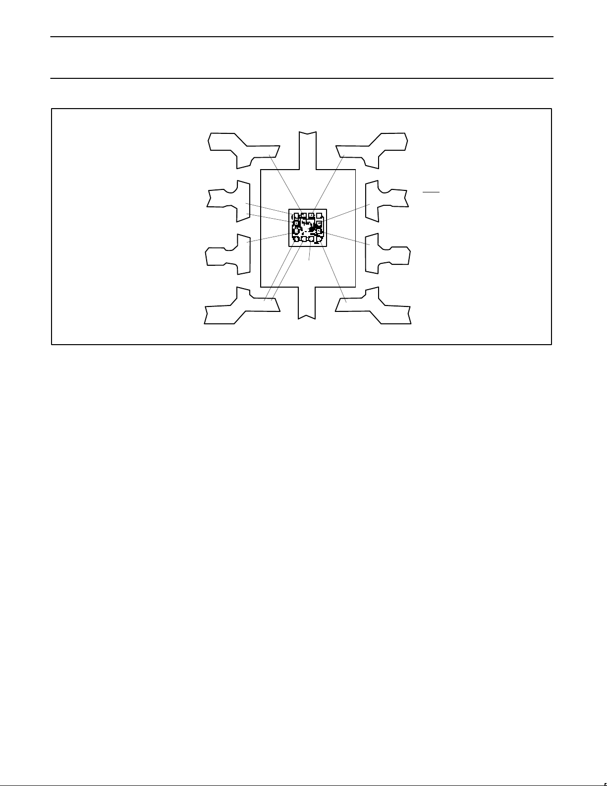
Figure 25. SA5222 Bonding Diagram
Die Sales Disclaimer
Due to the limitations in testing high frequency and other parameters
at the die level, and the fact that die electrical characteristics may
shift after packaging, die electrical parameters are not specified and
die are not guaranteed to meet electrical characteristics (including
temperature range) as noted in this data sheet which is intended
only to specify electrical characteristics for a packaged device.
All die are 100% functional with various parametrics tested at the
wafer level, at room temperature only (25°C), and are guaranteed to
be 100% functional as a result of electrical testing to the point of
wafer sawing only. Although the most modern processes are
utilized for wafer sawing and die pick and place into waffle pack
carriers, it is impossible to guarantee 100% functionality through this
process. There is no post waffle pack testing performed on
individual die.
Since Philips Semiconductors has no control of third party
procedures in the handling or packaging of die, Philips
Semiconductors assumes no liability for device functionality or
performance of the die or systems on any die sales.
Although Philips Semiconductors typically realizes a yield of 85%
after assembling die into their respective packages, with care
customers should achieve a similar yield. However, for the reasons
stated above, Philips Semiconductors cannot guarantee this or any
other yield on any die sales.
 Loading...