

Page 1
INTEGRATED CIRCUITS
IN
2
43 21
ENABLE IN
GND
AMP2
2
1
OUT
AMP1
GND
2
1
V
OUT
CC
8765
1
SA5200
RF dual gain-stage
Product Specification
Replaces data of Oct 10 1991
IC17 Data Handbook
Philips Semiconductors
1997 Nov 07
Page 2
Philips Semiconductors Product specification
SA5200RF dual gain-stage
DESCRIPTION
The SA5200 is a dual amplifier with DC to 1200MHz response. Low
noise (NF = 3.6dB) makes this part ideal for RF front-ends, and a
PIN CONFIGURATION
D Package
simple power-down mode saves current for battery operated
equipment. Inputs and outputs are matched to 50Ω.
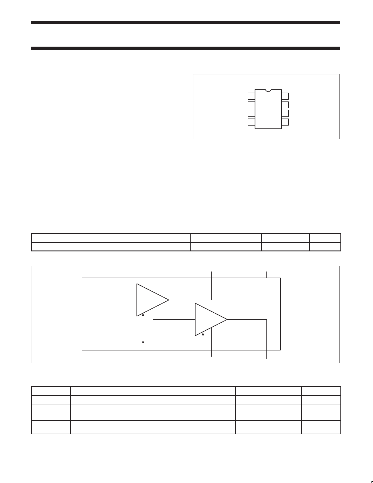
The enable pin allows the designer the ability to turn the amplifiers
on or off, allowing the part to act as an amplifier as well as an
attenuator. This is very useful for front-end buffering in receiver
applications.
FEATURES
•Dual amplifiers
•DC - 1200MHz operation
•Low DC power consumption (4.2mA per amplifier @ V
•Power-Down Mode (I
= 95µA typical)
CC
CC
= 5V)
•Supply voltage 4-9V
•Gain S
= 7dB at f = 1GHz
21
•Input and output match S
1
V
C
C
2
OUT
2
3
GND
2
45
IN
2
8
OUT
7
GND
6
IN
ENABLE
Figure 1. Pin Configuration
, S22 typically <–14dB
11
1
1
1
SR00166
•3.6dB noise figure at 900MHz
•Unconditionally stable
•Fully ESD protected
•Low cost
APPLICATIONS
•Cellular radios
•RF IF strips
•Portable equipment
ORDERING INFORMATION
DESCRIPTION TEMPERATURE RANGE ORDER CODE DWG #
8-Pin Plastic Small Outline (Surface–mount) –40-+85°C SA5200D SOT96-1
BLOCK DIAGRAM
IN
2
43 21
ENABLE
GND
2
AMP2
IN
1
Figure 2. Block Diagram
OUT
2
AMP1
GND
V
CC
8765
1
OUT
1
RECOMMENDED OPERATING CONDITIONS
SYMBOL PARAMETER RATING UNITS
V
CC
T
A
T
J
Supply voltage 4.0 to 9.0 V
Operating ambient temperature range
SA Grade
-40 to +85
Operating junction temperature
SA Grade
-40 to +105
SR00167
°C
°C
1997 Nov 07 853-1578 18662
5–2
Page 3
Philips Semiconductors Product specification
SYMBOL
PARAMETER
TEST CONDITIONS
UNITS
SYMBOL
PARAMETER
TEST CONDITIONS
UNITS
S21
Insertion gain
dB
S21
Insertion gain when disabled
dB
SA5200RF dual gain-stage
ABSOLUTE MAXIMUM RATINGS
SYMBOL PARAMETER RATING UNITS
V
T
P
T
CC
P
D
JMAX
MAX
STG
Supply voltage
Power dissipation, TA = 25°C (still air)
Maximum operating junction temperature 150 °C
Maximum power input/output +20 dBm
Storage temperature range –65 to +150 °C
NOTE:
1. Transients exceeding 10.5V on V
2. Maximum dissipation is determined by the operating ambient temperature and the thermal resistance, θ
8-Pin SO: θ
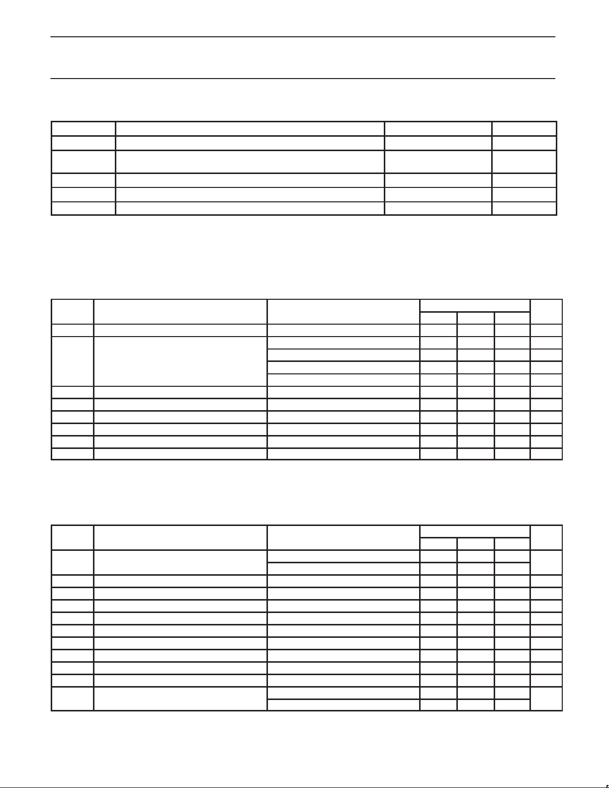
DC ELECTRICAL CHARACTERISTICS
VCC = +5V, TA = 25°C; unless otherwise stated.
V
I
V
V
V
IDC,ODC
NOTE:
1. The ENABLE input must be connected to a valid logic level for proper operation of the SA5200.
Supply voltage 4 5.0 9.0 V
CC
Total supply current VCC = 5V, ENABLE = Low 95 255 µA
CC
V
TTL/CMOS logic threshold voltage
T
Logic 1 level Power-up mode 2.0 V
IH
Logic 0 level Power-down mode -0.3 0.8 V
IL
I
Enable input current Enable = 0.4V -1 0 1 µA
IL
I
Enable input current Enable = 2.4V -1 0 1 µA
IH
Input and output DC levels 0.6 0.83 1.0 V
1
2
-0.5 to +9 V
8-Pin Plastic SO 780 mW
pin may damage product.
CC
= 158°C/W
JA
:
JA
LIMITS
MIN TYP MAX
VCC = 5V, ENABLE = High 6.4 8.4 10.4 mA
VCC = 9V, ENABLE = High 17.8 22.2 mA
VCC = 9V, ENABLE = Low 320 960 µA
1
1.25 V
CC
V
AC ELECTRICAL CHARACTERISTICS
VCC = +5V, TA = 25°C, either amplifier, enable = 5V; unless otherwise stated.
S22 Output return loss f = 900MHz –14.3 dB
S12 Reverse isolation f = 900MHz –17.9 dB
S11 Input return loss f = 900MHz –16.5 dB
P-1 Output 1dB compression point f = 900MHz –4.3 dBm
NF Noise figure in 50Ω f = 900MHz 3.6 dB
IP
2
IP
3
ISOL Amplifier-to-amplifier isolation
P
OUT
NOTE:
1. All measurements include the effects of the SA5200 Evaluation Board (see Figure 4). Measurement system impedance is 50Ω.
2. Input applied to one amplifier, output taken at the other output. All ports terminated into 50Ω.
1997 Nov 07
1
LIMITS
MIN TYP MAX
f = 100MHz 9.2 11 13.2
f = 900MHz 5.2 7.5
Input second-order intercept point f = 900MHz +4.3 dBm
Input third-order intercept point f = 900MHz –1.8 dBm
2
f = 900MHz –25 dB
Saturated output power f = 900MHz –1.7 dBm
f = 100MHz –13
f = 900MHz –13.5
5–3
Page 4

Philips Semiconductors Product specification
SA5200RF dual gain-stage
APPLICATIONS
SA5200 is a user-friendly, wide-band, unconditionally stable, low
power dual gain amplifier circuit. There are several advantages to
using the SA5200 as a high frequency gain block instead of a
discrete implementation. First is the simplicity of use. The SA5200
does not need any external biasing components. Due to the higher
level of integration and small footprint (SO8) package it occupies
less space on the printed circuit board and reduces the
manufacturing cost of the system. Also the higher level of
integration improves the reliability of the amplifier over a discrete
implementation with several components. The power down mode in
the SA5200 helps reduce power consumption in applications where
the amplifiers can be disabled. And last but not the least is the
impedance matching at inputs and outputs. Only those who have
toiled through discrete transistor implementations for 50Ω input and
output impedance matching can truly appreciate the elegance and
simplicity of the SA5200 input and output impedance matching to
50Ω.
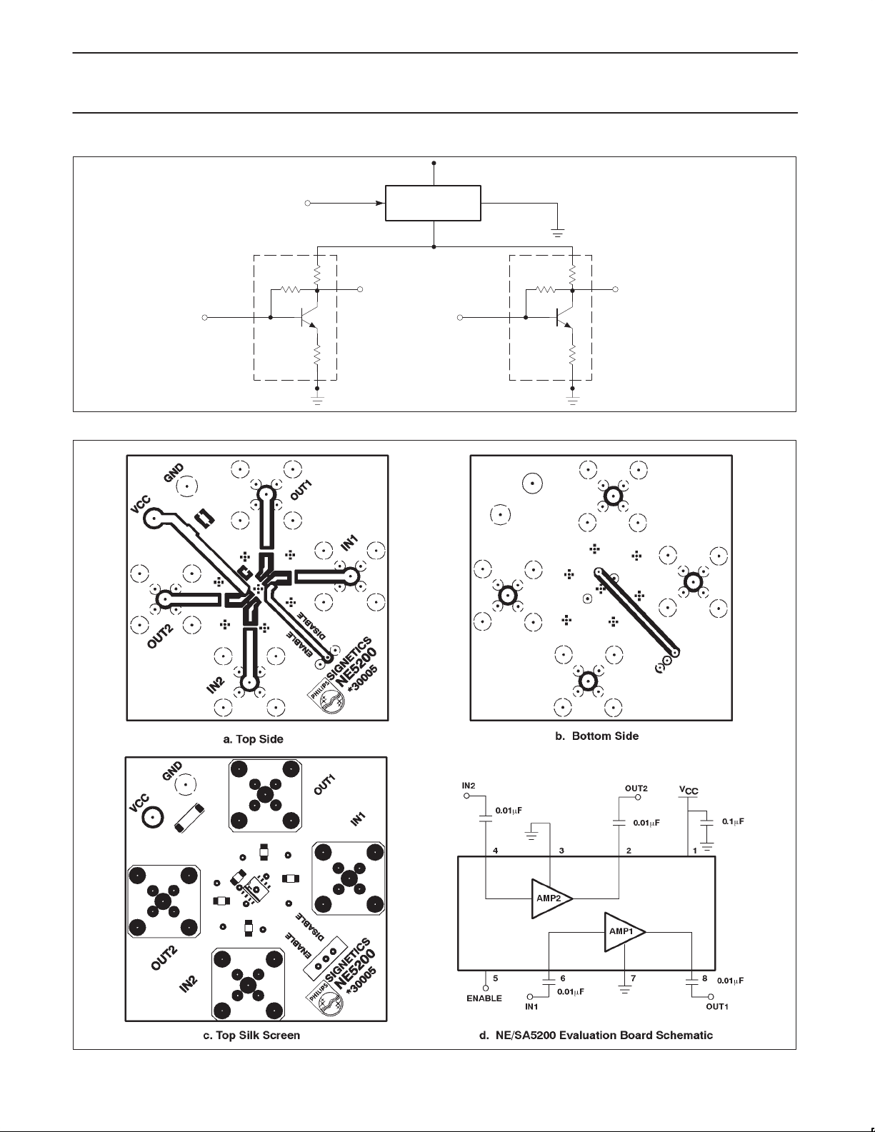
A simplified equivalent schematic is shown in 3. Each amplifier is
composed of an NPN transistor with an Ft of 13GHz in a classical
series-shunt feedback configuration. The two wideband amplifiers
are biased from the same bias generator. In normal operation each
amplifier consumes about 4mA of quiescent current (at V
In the disable mode the device consumes about 90µA of current,
most of it is in the TTL enable buffer and the bias generator. The
input impedance of the amplifiers is 50Ω. The amplifiers have
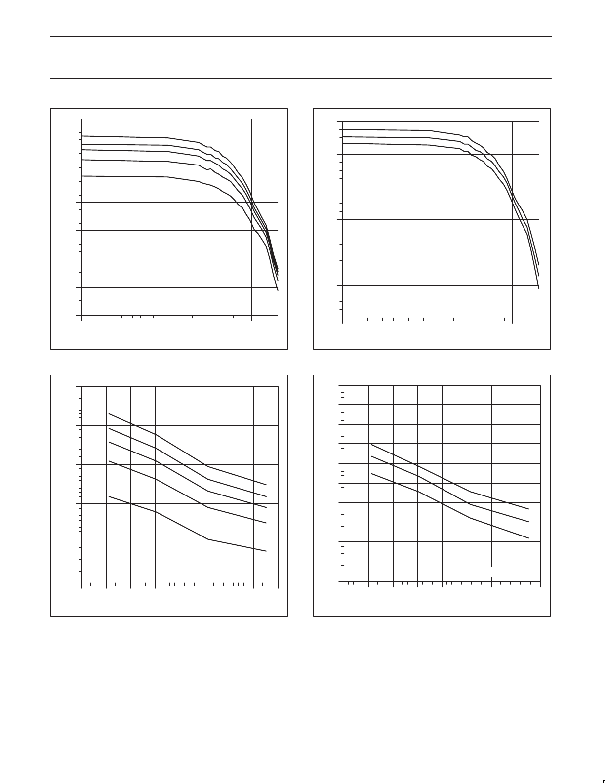
typical gain of 11dB at 100MHz and 7dB of gain at 1.2GHz.
It can be seen from 3 that any inductance between Pin 7, 3 and the
ground plane will reduce the gain of the amplifiers at higher
frequencies. Thus proper grounding of Pins 7 and 3 is essential for
maximum gain and increased frequency response. 4 shows the
printed circuit board layout and the component placement for the
SA5200 evaluation board. The AC coupling capacitors should be
selected such that at they are shorts at the desired frequency of
operation. Since most low-cost large value surface mount
capacitors cease to be simply capacitors in the UHF range and
exhibit an inductive behavior, it is recommended that high frequency
chip capacitors be utilized in the circuit. A good power supply
bypass is also essential for the performance of the amplifier and
should be as close to the device as practical.
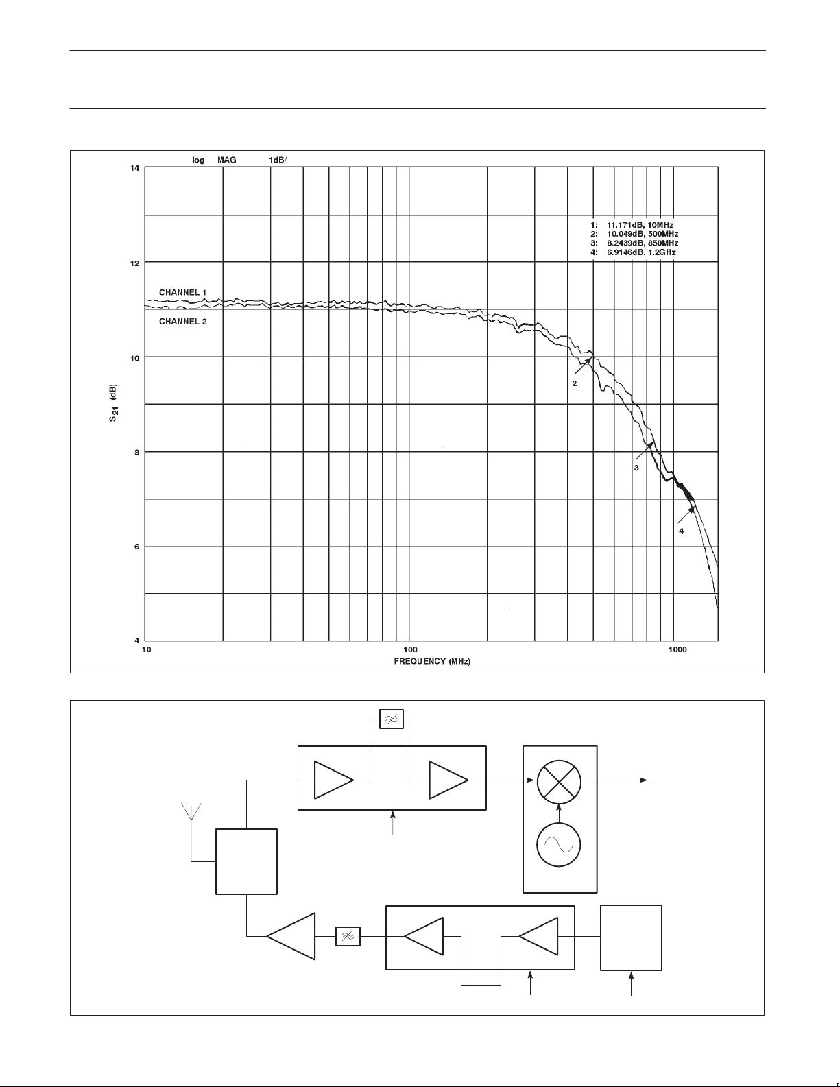
5 shows the typical frequency response of the two channels of
SA5200. The low frequency gain is about 11dB at 100MHz and
slowly drops off to 10dB at 500MHz. The gain is about 8dB at
900MHz and 7dB at 1.2 GHz which is typical of SA5200 with a good
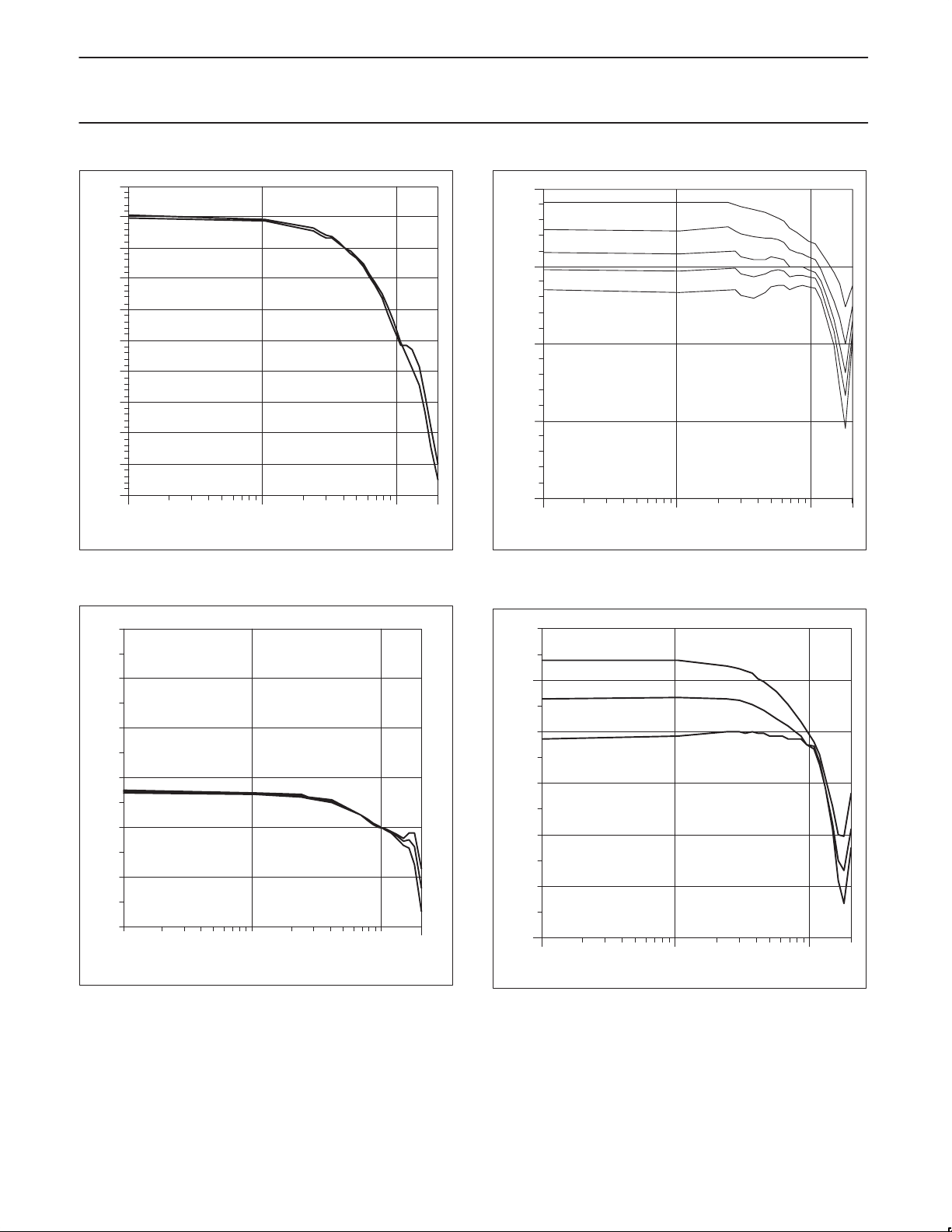
printed circuit board layout. It can also be seen that both channels
have a very well matched frequency response and matched gain to
within 0.1dB at 100MHz and 0.2dB at 900MHz.
CC
= 5V).
SA5200 finds applications in many areas of RF communications. It
is an ideal gain block for high performance, low cost, low power RF
communications transceivers. A typical radio transceiver front-end
is shown in 6. This could be the front-end of a cellular phone, a
VHF/ UHF hand-held transceiver, UHF cordless telephone or a
spread spectrum system. The SA5200 can be used in the receiver
path of most systems as an LNA and pre-amplifier. The bandpass
filter between the two amplifiers also minimize the noise into the first
mixer. In the transmitter path, SA5200 can be used as a buf fer to
the VCO and isolate the VCO from any load variations due to the
power level changes in the power amplifier. This improves the
stability of the VCOs. The SA5200 can also be used as a pre-driver
to the power amplifier modules.
The two amplifiers in SA5200 can be easily cascaded to have a
13dB gain block at 900MHz. At 100MHz the gain will be 22dB and a
noise figure of about 5.5dB. The SA5200 can be operated at a
higher voltage up to 9V for much improved 1dB output compression
point and higher 3rd order intercept point.
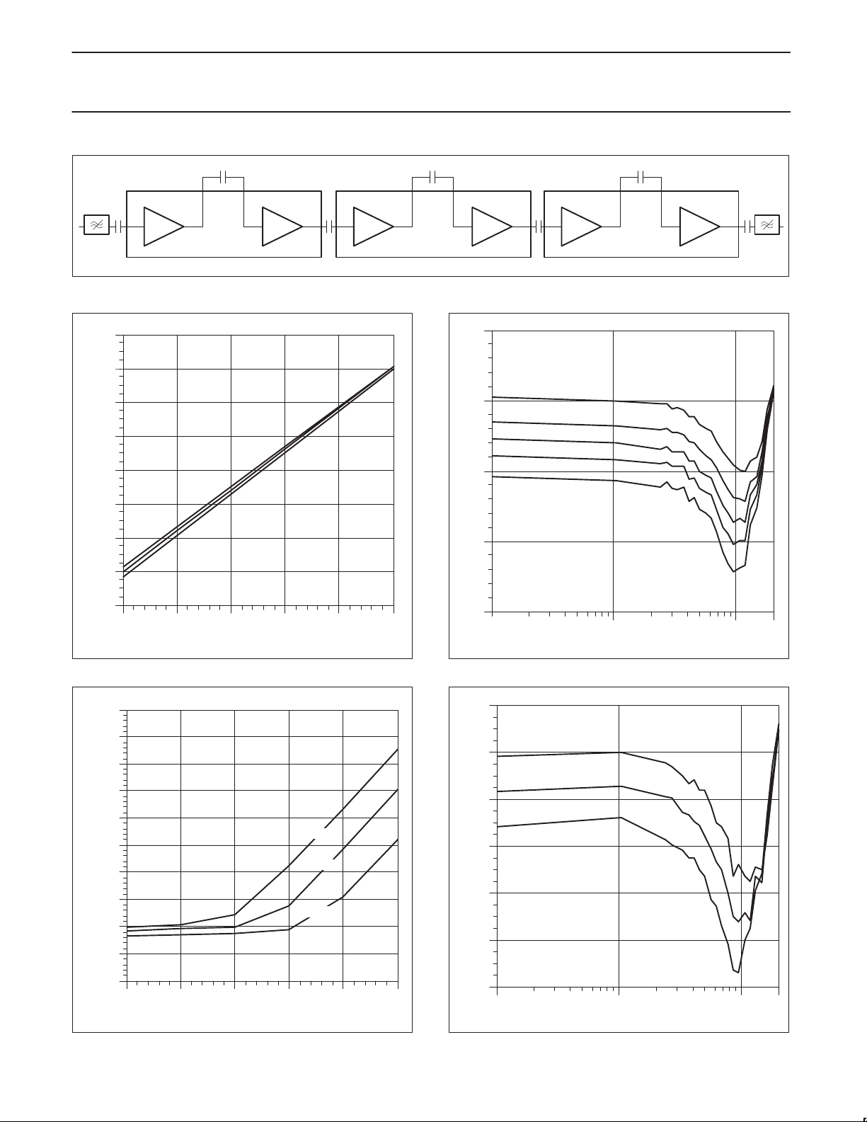
Several stages of SA5200 can also be cascaded and be used as an
IF amplifier strip for DBS/TV/GPS receivers. 7 shows a 60dB gain
IF strip at 180MHz. The noise figure for the cascaded amplifier
chain is given by equation 1.
NF (total) = NF1 + NF2/G1 + NF3/G1*G2 + NF4/G1*G2*G3 + ...
(Equation. 1)
NOTE: The noise figure and gain should not be in dB in the above
equation.
Since the noise figure for each stage is about 3.6dB and the gain is
about 11dB, the noise figure for the 60dB gain IF strip will be about
6.4dB.
In applications where a single amplifier is required with a 7.5dB gain
at 900MHz and current consumption is of paramount importance
(battery powered receivers), the amplifier A1 can be used and
amplifier A2 can be disabled by leaving GND2 (Pin 3) unconnected.
This will reduce the total current consumption for the IC to a meager
4mA.
The ENABLE pin is useful for Time-Division-Duplex systems where
the receiver can be disabled for a period of time. In this case the
overall system supply current will be decreased by 8mA.
The ENABLE pin can also be used to improve the system dynamic
range. For input levels that are extremely high, the SA5200 can be
disabled. In this case the input signal is attenuated by 13dB. This
prevents the system from being overloaded as well as improves the
system’s overall dynamic range. In the disabled condition the
SA5200 IP
increases to nearly +20dBm.
3
1997 Nov 07
5–4
Page 5
Philips Semiconductors Product specification
SA5200RF dual gain-stage
PIN 1
V
CC
PIN 6
IN1
AMP1
PIN 5
ENABLE
R
F
R
C
PIN 8
OUT1
R
E
PIN 7
GND1
BIAS
GENERATOR
PIN 4
IN2
Figure 3. Simplified Equivalent Schematic of SA5200
AMP2
GND1
R
F
R
C
PIN 2
OUT2
R
E
PIN 3
GND2
SR00168
1997 Nov 07
SR00169
Figure 4. Printed Circuit Board Layout of the SA5200 Evaluation Board
5–5
Page 6
Philips Semiconductors Product specification
SA5200RF dual gain-stage
1997 Nov 07
ANTENNA
Figure 5. Typical Frequency Response of SA5200 in a 50Ω System
FILTER
NE5200
ENABLE
Rx
DUPLEX
FILTER
NE602A
NE5200
POWER
AMP
FILTER
ENABLE
Figure 6. Typical Radio Transceiver Front-End
5–6
SR00170
IF OUT
LO
VCO
Tx
MODULATION
SR00171
Page 7
Philips Semiconductors Product specification
SA5200RF dual gain-stage
IF IN
NE5200
Figure 7. 60dB IF Gain Block for 100-300MHz IF for GPS/DBS Systems
20
18
16
14
12
CC
I (mA)
10
8
6
4
456789
+85°C
–40°C
(V)
V
CC
SR00173
Figure 8. Supply Current vs Supply Voltage and Temperature
NE5200NE5200
-5
4V
-10
5V
6V
7V
-15
9V
11
S (dB)
-20
= +25°C
T
A
-25
10 100 1000 2000
FREQUENCY (MHz)
IF OUT
Figure 10. Input Match vs Frequency and V
IF OUT
SR00172
SR00174
CC
500
450
400
350
300
µ
250
CC
I ( A)
200
150
100
50
0
456789
V
CC
+85°C
+25°C
–40°C
(V)
SR00175
Figure 9. Disabled Supply Current vs VCC and Temperature
1997 Nov 07
5–7
-8
-10
-12
-14
11
S (dB)
-16
-18
-20
10 100 1000 2000
+85°C
+25°C
-40°C
= 5V
V
CC
FREQUENCY (MHz)
Figure 11. Input Match vs Frequency and Temperature
SR00176
Page 8
Philips Semiconductors Product specification
SA5200RF dual gain-stage
14
9V
12
10
8
21
S (dB)
6
4
2
0
10 100 1000 2000
7V
6V
5V
4V
TA = +25°C
FREQUENCY (MHz)
Figure 12. Insertion Gain vs Frequency and V
10
SR00177
CC
12
10
8
6
21
S (dB)
4
2
0
10 100 1000 2000
-40°C
+25°C
+85°C
FREQUENCY (MHz)
= 5V
V
CC
SR00180
Figure 14. Insertion Gain vs Frequency and Temperature
10
9.5
9
8.5
8
21
S (dB)
7.5
7
6.5
6
8009V850 900 950 1000 1050 1100 1150 1200
7V
6V
5V
4V
TA = +25°C
FREQUENCY (MHz)
Figure 13. Insertion Gain vs Frequency and V
— Expanded Detail —
SR00178
CC
9.5
9
8.5
8
7.5
21
S (dB)
7
6.5
6
5.5
5
800
850 900 950 1000 1050 1100 1150 1200
-40°C
+25°C
+85°C
FREQUENCY (MHz)
VCC = 5V
SR00179
Figure 15. Insertion Gain vs Frequency and Temperature
– Expanded Detail –
1997 Nov 07
5–8
Page 9
Philips Semiconductors Product specification
SA5200RF dual gain-stage
12
11
10
9
8
7
21
S (dB)
6
5
4
3
2
10 100 1000 2000
FREQUENCY (MHz)
V
CC
T
= +25°C
A
= 5V
Figure 16. Insertion Gain Matching
(CH1 vs CH2) vs Frequency
-10
-12
CH1
CH2
SR00181
-10
-15
-20
22
S (dB)
-25
-30
10 100 1000 2000
9V
7V
6V
5V
4V
= +25°C
T
A
FREQUENCY (MHz)
Figure 18. Output Match vs Frequency and V
-10
+85°C
-12
+25°C
SR00182
CC
-14
12
-16
S (dB)
-18
-20
-22
10 100 1000 2000
FREQUENCY (MHz)
V
= 5V
CC
Figure 17. Reverse Insertion Gain vs Frequency and
Temperature
+85°C
-40°C
SR00183
+25°C
-14
-16
22
S (dB)
-18
-20
-22
10 100 1000 2000
-40°C
V
CC
FREQUENCY (MHz)
= 5V
SR00184
Figure 19. Output Match vs Frequency and Temperature
1997 Nov 07
5–9
Page 10
Philips Semiconductors Product specification
SA5200RF dual gain-stage
-0
S11
S22
-5
-10
V
CC
T
= +25°C
A
S12
S21
= 5V
S (dB)
-15
-20
-25
10 100 1000 2000
FREQUENCY (MHz)
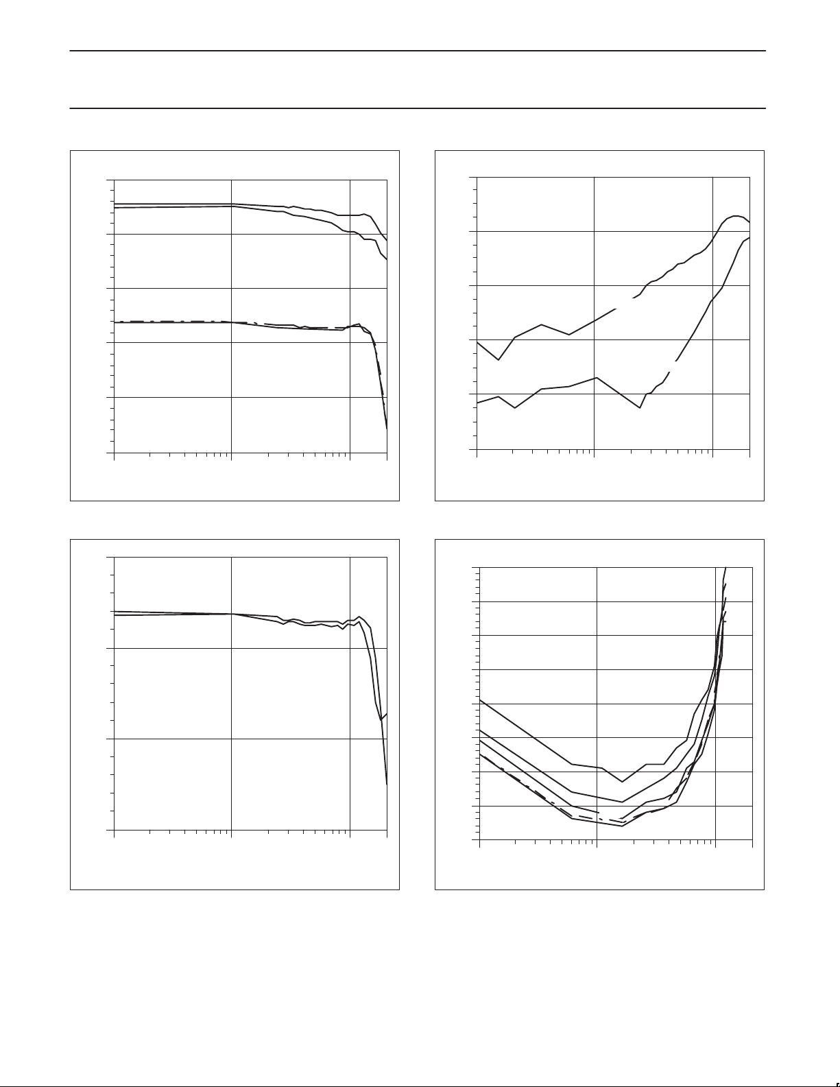
Figure 20. S-parameters vs Frequency for Disabled Amplifier
-10
0
-20
-40
ENABLED
21
S (dB)
-60
DISABLED
-80
V
= 5V
CC
T
= +25°C
-100
10 100 1000 2000
FREQUENCY (MHz)
A
Figure 22. CH1 Input to CH2 Output Isolation vs Frequency
4
CH2
CH1
-15
21
S (dB)
-20
= 5V
V
CC
TA = +25°C
-25
10 100 1000 2000
FREQUENCY (MHz)
Figure 21. Insertion Gain Matching Disabled (CH1 vs CH2) vs
Frequency
3.9
T
= +25°C
A
3.8
3.7
3.6
NF (dB)
3.5
4V
3.4
3.3
3.2
10 100 1000 2000
9V
5V
6V & 7V
FREQUENCY (MHz)
Figure 23. Noise Figure vs Frequency and VCC in a 50Ω System
1997 Nov 07
5–10
Page 11
Philips Semiconductors Product specification
SA5200RF dual gain-stage
5
T
= +25°C
A
9V
0
7V
-1
P (dBm)
-5
-10
10 100 1000 2000
6V
5V
4V
FREQUENCY (MHz)
SR00185
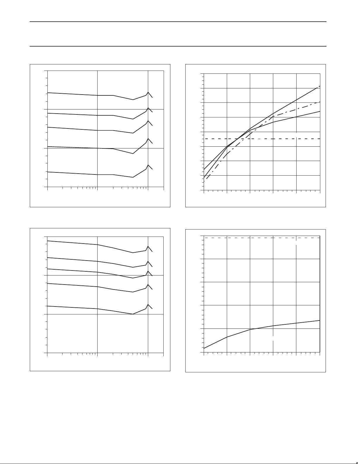
Figure 24. 1dB Output Compression Point vs Frequency and
V
CC
5
9V
16
14
12
10
8
3
IP (dBm)
6
4
2
0
= +25°C
T
A
4
56789
VCC (V)
100MHz
500MHz
900MHz
DISABLED
SR00186
Figure 26. Third-Order Output Intercept vs Frequency and V
20
DISABLED
CC
7V
= +25°C
T
A
6V
5V
4V
SR00187
0
SAT
P (dBm)
-5
-10
10 100 1000 2000
FREQUENCY (MHz)
Figure 25. Saturated Output Power vs Frequency and V
CC
15
10
3
IP (dBm)
5
0
f = 900MHz
= +25°C
T
A
-5
4
56789
(V)
V
CC
SR00188
Figure 27. Third-Order Input Intercept vs Frequency and V
CC
1997 Nov 07
5–11
Page 12
Philips Semiconductors Product specification
SA5200RF dual gain-stage
25
20
15
900MHz
2
IP (dBm)
10
500MHz
5
100MHz
0
456789
(V)
V
CC
= +25°C
T
A
DISABLED
SR00191
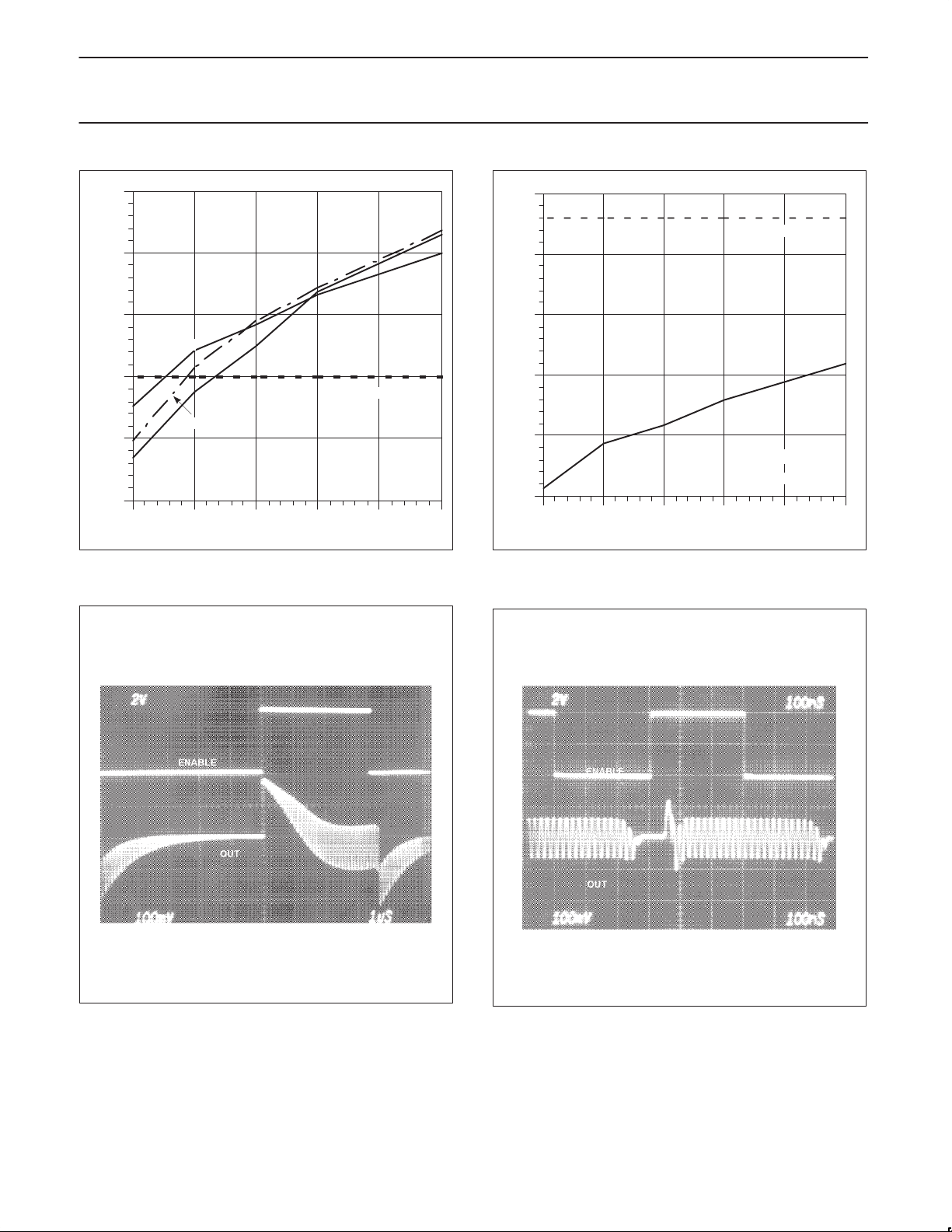
Figure 28. Second-Order Output Intercept vs Frequency and
V
CC
25
DISABLED
20
15
2
IP (dBm)
10
5
TA = +25°C
f = 900MHz
0
4
56789
VCC (V)
SR00190
Figure 30. Second-Order Input Intercept vs Frequency and V
CC
ENABLE
OUT
SR00189
Figure 29. Switching Speed; fIN = 10MHz at –26dBm, VDD = 5V,
Coupling Capacitors Set to 0.01µF
ENABLE
ENABLE
OUT
OUT
SR00192
Figure 31. Switching Speed; fIN = 50MHz at –26dBm,
V
= 5V, Coupling Capacitors Set to 100pF
DD
1997 Nov 07
5–12
Page 13
Philips Semiconductors Product specification
SA5200RF dual gain-stage
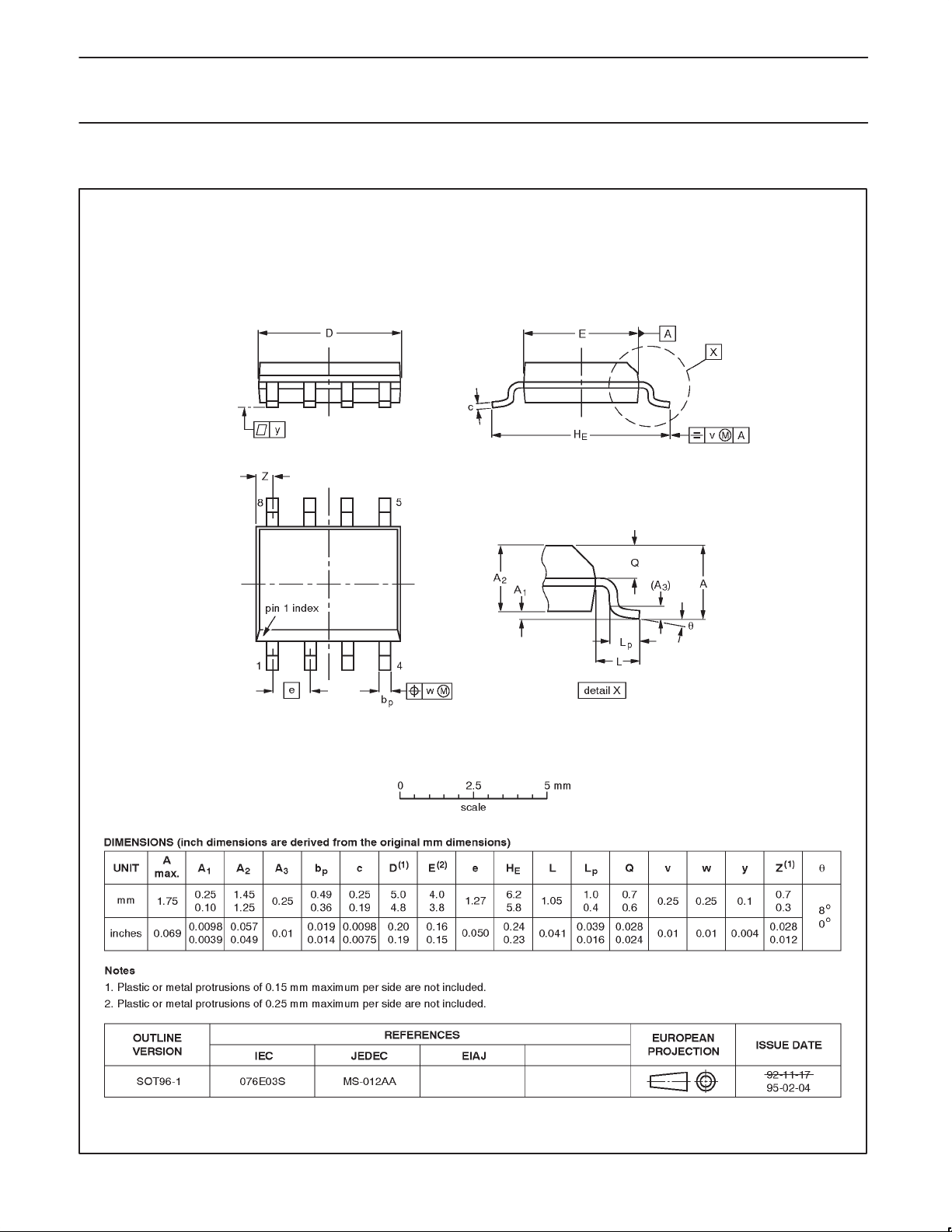
SO8: plastic small outline package; 8 leads; body width 3.9mm SOT96-1
1997 Nov 07
13
Page 14

Philips Semiconductors Product specification
SA5200RF dual gain-stage
DEFINITIONS
Data Sheet Identification Product Status Definition
Objective Specification
Preliminary Specification
Product Specification
Formative or in Design
Preproduction Product
Full Production
Philips Semiconductors and Philips Electronics North America Corporation reserve the right to make changes, without notice, in the products,
including circuits, standard cells, and/or software, described or contained herein in order to improve design and/or performance. Philips
Semiconductors assumes no responsibility or liability for the use of any of these products, conveys no license or title under any patent, copyright,
or mask work right to these products, and makes no representations or warranties that these products are free from patent, copyright, or mask
work right infringement, unless otherwise specified. Applications that are described herein for any of these products are for illustrative purposes
only. Philips Semiconductors makes no representation or warranty that such applications will be suitable for the specified use without further testing
or modification.
LIFE SUPPORT APPLICA TIONS
Philips Semiconductors and Philips Electronics North America Corporation Products are not designed for use in life support appliances, devices,
or systems where malfunction of a Philips Semiconductors and Philips Electronics North America Corporation Product can reasonably be expected
to result in a personal injury. Philips Semiconductors and Philips Electronics North America Corporation customers using or selling Philips
Semiconductors and Philips Electronics North America Corporation Products for use in such applications do so at their own risk and agree to fully
indemnify Philips Semiconductors and Philips Electronics North America Corporation for any damages resulting from such improper use or sale.
Philips Semiconductors
811 East Arques Avenue
P.O. Box 3409
Sunnyvale, California 94088–3409
Telephone 800-234-7381
This data sheet contains the design target or goal specifications for product development. Specifications
may change in any manner without notice.
This data sheet contains preliminary data, and supplementary data will be published at a later date. Philips
Semiconductors reserves the right to make changes at any time without notice in order to improve design
and supply the best possible product.
This data sheet contains Final Specifications. Philips Semiconductors reserves the right to make changes
at any time without notice, in order to improve design and supply the best possible product.
Philips Semiconductors and Philips Electronics North America Corporation
register eligible circuits under the Semiconductor Chip Protection Act.
Copyright Philips Electronics North America Corporation 1993
All rights reserved. Printed in U.S.A.
1997 Nov 07
14
 Loading...