

Page 1
H/BRIDGE MOTOR DRIVER/AMPLIFIER
MICROTECHNOLOGY
HTTP://WWW.APEXMICROTECH.COM (800) 546-APEX (800) 546-2739
FEA TURES
• LOW COST COMPLETE H-BRIDGE
• SELF-CONTAINED SMART LOWSIDE/HIGHSIDE DRIVE
CIRCUITRY
• SINGLE SUPPLY OPERATION
• WIDE SUPPLY RANGE: UP TO 80V
• 5A CONTINUOUS OUTPUT
• HERMETIC SEALED PACKAGE
• HIGH EFFICIENCY: 97%
• FOUR QUADRANT OPERATION, TORQUE
CONTROL CAPABILITY
• INTERNAL PWM GENERATION
APPLICATIONS
• BRUSH TYPE MOTOR CONTROL
• CLASS D SWITCHMODE AMPLIFIER
• REACTIVE LOADS
• MAGNETIC COILS (MRI)
• ACTIVE MAGNETIC BEARING
• VIBRATION CANCELLING
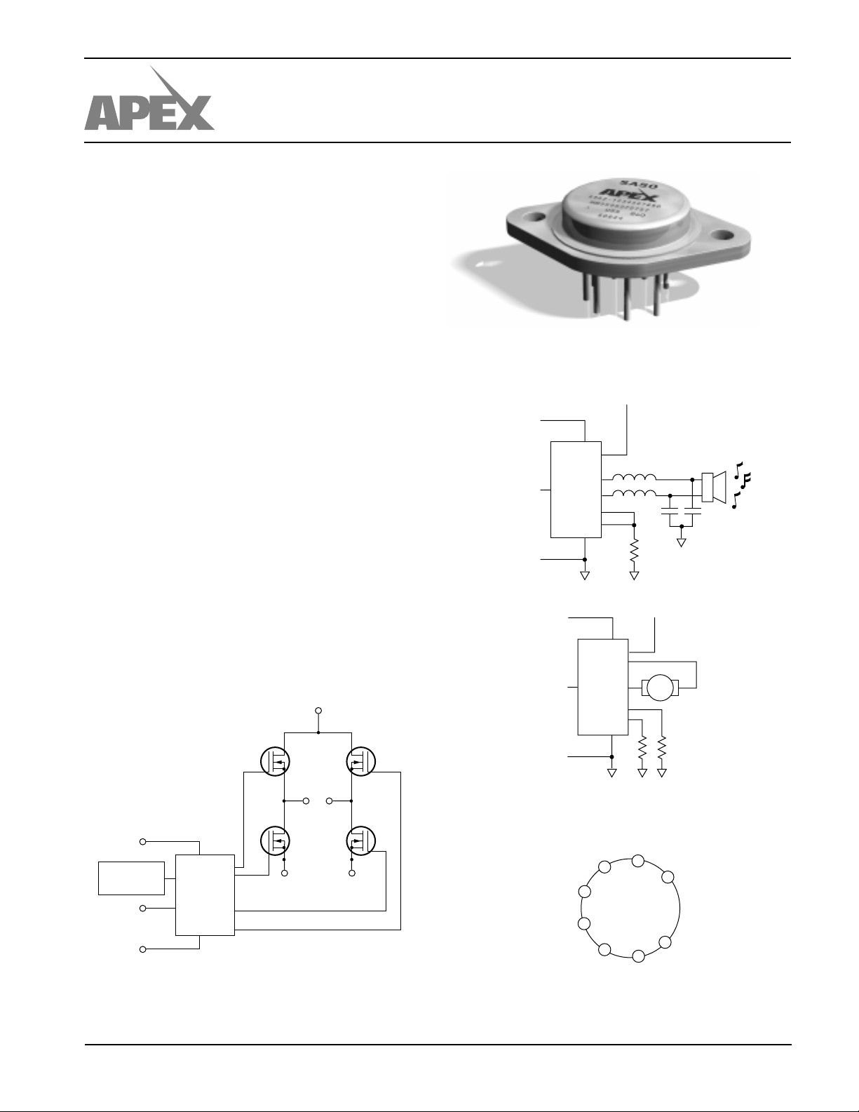
SA50
TYPICAL APPLICATION
Vcc
AUDIO
INPUT
SA50
+V
S
DESCRIPTION
The SA50 is a pulse width modulation amplifier that can
supply 5A continuous current to the load. The full bridge
amplifier can be operated over a wide range of supply voltages. All of the drive/control circuitry for the lowside and
highside switches are internal to the hybrid. The PWM circuitry
is internal as well, leaving the user to only provide an analog
signal for the motor speed/direction, or audio signal for
switchmode audio amplification. The SA50 is packaged in a
space efficient isolated 8-pin TO-3 that can be directly connected to a heatsink.
+V
BLOCK DIAGRAM
V
CC
(+12V)
45KHz
PWM
GENERATOR
INPUT
GND
H-BRIDGE
CIRCUITRY
DRIVE
RSENSE B
S
(LOAD)
BA
RSENSE A
(CURRENT)
GND
Vcc
ANALOG
INPUT
GND
SA50
EXTERNAL CONNECTIONS
+V
S
3
A OUT
RSENSE A
4
TOP VIEW
5
6
Vcc
GND
+V
B OUT
2
7
S
DC MOTOR
RSENSE B
1
8
INPUT
SPEAKER
APEX MICROTECHNOLOGY CORPORATION • TELEPHONE (520) 690-8600 • FAX (520) 888-3329 • ORDERS (520) 690-8601 • EMAIL prodlit@apexmicrotech.com
Page 2

SA50
ABSOLUTE MAXIMUM RATINGS
SPECIFICATIONS
ABSOLUTE MAXIMUM RATINGS
SUPPLY VOLTAGE, +V
OUTPUT CURRENT, peak 7A
LOGIC SUPPLY VOLTAGE, Vcc 16V
POWER DISSIPATION, internal 120W
TEMPERATURE, pin solder - 10s 300°C
TEMPERATURE, junction
TEMPERATURE, storage –65 to +150°C
OPERATING TEMPERATURE RANGE, case –65 to +125°C
INPUT VOLTAGE +1 to Vcc – 1.5 Vdc
S
3
80V
1
150°C
SPECIFICATIONS
PARAMETER TEST CONDITIONS
INPUT
ANALOG INPUT VOLTAGES Vcc = 12V
MOTOR A, B = 50% Duty Cycle 6 Vdc
MOTOR A = 100% Duty Cycle High 8 Vdc
MOTOR B = 100% Duty Cycle High 4 Vdc
OUTPUT
Vds (ON) VOLTAGE, each MOSFET Ids = 5A 1.25 1.8 Vdc
TOTAL Ron, both MOSFETs 0.5 Ω
EFFICIENCY, 5A OUTPUT +VS = 80V 97 %
SWITCHING FREQUENCY 40 45 50 Khz
CURRENT, continuous 5 A
CURRENT, peak t = 100 msec 7 A
SWITCHING CHARACTERISTICS
RISE TIME 36 54 nS
FALL TIME 170 250 nS
DEAD TIME 100 nS
4
+VS = 28V, Vcc = 12V, Ic =2A
2
MI N TYP MAX UNITS
POWER SUPPLY
+VS VOLTAGE +VS Current = Load Current 80 Vdc
Vcc VOLTAGE 9 12 16 Vdc
Vcc CURRENT Vcc = 12Vdc 15 20 mA
THERMAL
RESISTANCE, junction to case Full temp range, for each transistor 2.0 °C/W
RESISTANCE, junction to air Full temperature range 30 °C/W
TEMPERATURE RANGE, case –25 +85 °C
NOTES: 1. Each of the two active output transistors can dissipate 60W.
CAUTION
3
2. Unless otherwise noted: TC = 25°C, Vcc = 12Vdc.
3. Long term operation at the maximum junction temperature will result in reduced product life. Derate internal power
dissipation to achieve high MTTF. For guidance, refer to the heatsink data sheet.
4. Guaranteed but not tested.
The SA50 is constructed from MOSFET transistors. ESD handling procedures must be observed.
The internal substrate contains beryllia (BeO). Do not break the seal. If accidentally broken, do not crush, machine, or
subject to temperatures in excess of 850°C to avoid generating toxic fumes.
WARNING—AMPLIFIER PROTECTION
The SA50 contains an internal logic chip that turns on and
turns off output MOSFET drivers at a certain sequence. Noises
or oscillation caused by external wiring inductance, lack of
proper power supply bypass capacitors, ground, supply and
local internal loops, may be fed back to this logic chip and
cause it to turn on one or more MOSFET drivers at the wrong
time, thus destroying the SA50. A well laid out PC board with
low impedance copper ground plane is necessary for the
SA50 to function properly. The Apex EK-SA50 evaluation
board is recommended for fast and easy breadboarding of
circuits using the SA50.
APEX MICROTECHNOLOGY CORPORATION • 5980 NORTH SHANNON ROAD • TUCSON, ARIZONA 85741 • USA • APPLICATIONS HOTLINE: 1 (800) 546-2739
Page 3

TYPICAL PERFORMANCE
GRAPHS
SA50
60
POWER DERATING
50
INPUT CURRENT VS TEMP
1.05
0.95
0.85
40
30
20
0.75
0.65
0.55
0.45
10
EACH OUTPUT TRANSISTOR
0
INTERNAL POWER DISSIPATION, (W)
CASE TEMPERATURE, T (°C)
EFFICIENCY VS TEMP @ 80V EFFICIENCY VS TEMP @ 20V
100
99
I
98
97
I
OUT
96
95
EFFICIENCY, (%)
94
= 1A, V
OUT
= 5A, V
75
S
= 80V
1000 25 50 125
= 80V
S
C
93
92
–60 180–20 20 60 100 140
JUNCTION TEMPERATURE (°C)
PWM BIAS CURRENT, (µA)
0.35
0.25
–40 120
–20 0 20 40 60 80 100 4 5
CASE TEMPERATURE, (°C)
100
95
I
OUT
= 1A, V
90
85
I
OUT
= 5A, V
80
75
EFFICIENCY, (%)
70
65
–60 180
–20 20 60 100 140
JUNCTION TEMPERATURE (°C)
S
= 20V
= 20V
S
EFFICIENCY CONTOURS
80
(V)
S
70
60
50
97%
95%
40
30
20
SUPPLY VOLTAGE, V
10
0
123
90%
80%
70%
LOAD CURRENT, (A)
EFFICIENCY VS LOAD CURRENT
100
V
= 80V
V
V
S
S
V
= 60V
S
= 40V
S
= 20V
97
94
91
EFFICIENCY, (%)
88
85
12345
LOAD CURRENT, (A)
OUTPUT RESISTANCE DRIFT
2.5
2
1.5
1
0.5
0
–60 180–20 20 60 100 140
OUTPUT RESISTANCE, (NORMALIZED)
JUNCTION TEMPERATURE (°C)
VOLTAGE DROP (BOTH MOSFETS)
5
CASE TEMPERATURE
4
3
2
VOLTAGE DROP, (V)
1
0
051234
85°C
110°C
60°C
35°C
OUTPUT CURRENT, (A)
H-BRIDGE FET CAPACITANCE
500
400
300
200
100
DRAIN-TO-SOURCE CAP, (pF)
0
1 2 5 10 20 50 100
DRAIN-TO-SOURCE VOLTAGE, (V)
QUIESCENT CURRET VS PWM FREQ
15
14
13
12
11
QUIESCENT CURRENT, (mA)
10
0
200
400 600
PWM FREQUENCY (Hz)
QUIESCENT CURRENT VS VOLTAGE
14.0
12.0
10.0
8.0
6.0
4.0
QUIESCENT CURRENT, (mA)
2.0
8 9 10 11 13 1512 14
Vcc VOLTAGE (V)
APEX MICROTECHNOLOGY CORPORATION • TELEPHONE (520) 690-8600 • FAX (520) 888-3329 • ORDERS (520) 690-8601 • EMAIL prodlit@apexmicrotech.com
Page 4

SA50
OPERATING
CONSIDERATIONS
GENERAL
Helpful information about power supplies, heatsinking and
mounting can be found in the “General Operating Considerations” section of the Apex data book. For information on the
package outline, heatsinks, and mounting hardware see the
“Package Outlines” and “Accessories” section of the data
book. Also see Application Note 30 on “PWM Basics.”
PIN DESCRIPTION
VCC - is the low voltage supply for powering internal logic
and drivers for the lowside and highside MOSFETS. The
supplies for the highside drivers are derived from this voltage.
V
- is the higher voltage H-bridge supply. The MOSFETS
S
obtain the output current from this supply pin. The voltage on
this pin is limited to +80V by the drive IC. The MOSFETS are
rated at 100 volts. Proper by-passing to GND with sufficient
capacitance to suppress any voltage transients, and to ensure
removing any drooping during switching, should be done as
close to the pins on the hybrid as possible.
A OUT - is the output pin for one half of the bridge. Increasing
the input voltage causes increasing duty cycle at this output.
B OUT - is the output pin for the other half of the bridge.
Decreasing the input voltage causes increasing duty cycles at
this point.
RSENSE A - This is the connection for the bottom of the A
half bridge. This can have a sense resistor connected to the V
return ground for current limit sensing, or can be connected
directly to ground. The maximum voltage on this pin is ±2 volts
with respect to GND.
GND - is the return connection for the input logic and Vcc.
RESENSE B - This is the connection for the bottom of the B
half bridge. This can have a sense resistor connection to the
V
return ground for current limit sensing, or can be connected
S
directly to ground. The maximum voltage on this pin is ±2 volts
with respect to GND.
INPUT - is an analog input for controlling the PWM pulse
width of the bridge. A voltage higher than Vcc/2 will produce
greater than 50% duty cycle pulses out of A OUT. A voltage
lower than Vcc/2 will produce greater than 50% duty cycle
pulses out of B OUT.
TYPICAL SYSTEM OPERATION
+V
+V
S
3
S
4
2
5
1
RIN
Rf
SNUBBER NETWORK
100Ω
2W
1000pF
200V
+12V
MOTOR
SENSE
RESISTORS
0.1Ω
RDIVIDE
RDIVIDE
RIN
and negative spikes
S
+12V
6
GND
Vcc
MOTOR A
SA50
8
INPUT
MOTOR B
7
GND
RSENSE A
RSENSE B
NO OUTPUT
SWITCHING
CURRENT
CURRENT CONTROL
22µF
R
R
+12V
ANALOG
INPUT
S
This is a diagram of a typical application of the SA50. The
design Vcc voltage is +12 volts and should have a good low
ESR bypass capacitor such as a tantalum electrolytic. The
analog input can be an analog speed control voltage from a
potentiometer, other analog circuitry or by microprocessor and
a D/A converter. This analog input gets pulled by the current
control circuitry in the proper direction to reduce the current
flow in the bridge if it gets too high. The gain of the current
control amplifier will have to be set to obtain the proper amount
of current limiting required by the system.
Current sensing is done in this case by a 0.1Ω sense resistor
to sense the current from both legs of the bridge separately. It
is important to make the high current traces as big as possible
to keep inductance down. The storage capacitor connected to
the V
and the hybrid GND should be large enough to provide
S
the high energy pulse without the voltage sagging too far. A
low ESR capacitor will be required. Mount capacitor as close
to the hybrid as possible. The connection between GND and
the V
return should not be carrying any motor current. The
S
sense resistor signal is common mode filtered as necessary to
feed the limiting circuitry. This application will allow full four
quadrant torque control for a closed loop servo system.
A snubber network is usually required, due to the inductance
in the power loop. It is important to design the snubber network
to suppress any positive spikes above +V
below –2V with respect to pin 7 (GND).
MYLAR
(VCC÷2)
6.8µF
100V
POLY
RDIVIDE = 2X Rf
This data sheet has been carefully checked and is believed to be reliable, however, no responsibility is assumed for possible inaccuracies or omissions. All specifications are subject to change without notice.
APEX MICROTECHNOLOGY CORPORATION • 5980 NORTH SHANNON ROAD • TUCSON, ARIZONA 85741 • USA • APPLICATIONS HOTLINE: 1 (800) 546-2739
SA50U REV. D JANUARY 1998 © 1998 Apex Microtechnology Corp.
 Loading...