

Page 1

INTEGRATED CIRCUITS
SA1620
Low voltage GSM front-end transceiver
Product specification
Supersedes data of 1996 Oct 08
IC17 Data Handbook
1997 May 22
Page 2

Philips Semiconductors Product specification
SA1620Low voltage GSM front-end transceiver
DESCRIPTION
The SA1620 is a combined receive (Rx) and transmit (Tx) front-end
for GSM cellular telephones. The receive path contains two low
noise amplifiers (LNA1 and LNA2) with four switchable attenuation
steps. A Gilbert Cell mixer in the receive path down-converts the
RF signal to a first IF of 70 to 500 MHz. A second Gilbert Cell in the
transmit path transposes a GMSK or phase modulated IF to RF by
image reject mixing and has a fixed IF of 400 MHz. A buffered LO
signal is fed to Rx and Tx mixers. Rx or Tx path or the entire circuit
may be powered-down.
FEA TURES
•Excellent noise figure: <2dB for the LNAs at 950MHz
•LNAs matched to 50Ω with external matching components
•LNAs with gain control, 59dB dynamic range in four discrete steps
•LNA gain stability ±0.5dB within -40 to 85°C
PIN CONFIGURATION
LQFP Package
VccL1
OUT1
GNDL1A
GNDL1
45464748
1
V
CCL2
2
IN2
3
GNDL2
OUT2
INM
INMX
COMP2
COMP1
BM
CC
4
5
6
B
7
A
8
9
10
11
12
13 14 15 16 17 18 19
GNDL2A
V
•Feedthrough attenuation LNA1 to Rx mixer ≥ 35dB
•Tx power adjustable from -3 to +12dBm by external resistor
•Direct supply: 2.7V to 5.5V
•Battery supply voltage V
= 3.3V to 7.5V or direct supply
BATT
•Two DC regulators programmable for 3.0V, 3.4V, 3.7V or 5.1V
•Low current consumption: 28mA for Rx or 59mA for Tx
•Fully compatible with SA1638 GSM IF Digital I/Q circuit
APPLICATIONS
•900MHz front end for GSM hand-held units
•Portable radio, TDMA systems
IN1
RETx
GNDTx3
TxO
Tx0X
GNDTx4
PDTx
424344
48–PIN LQFP
394041 3738
20 21 22 23 24
PONBUF
36
35
34
33
32
31
30
29
28
27
26
25
V
BATT
PON
GNDREG1
VREG1
VREGF2
VREG2
GNDREG2
CON1
LO INX
LO IN
CON2
GNDTx2
PONRx
GNDBM
GND1
RxIF
RxIFX
GND2
TxIF
TxIFX
GND3
VccTx1
GNDTx1
VccTx2
SR00127
Figure 1. Pin Configuration
ORDERING INFORMATION
DESCRIPTION TEMPERATURE RANGE ORDER CODE DWG #
48-Pin Thin Quad Flat Pack (TQFP)
-40 to +85°C
SA1620BE SOT313-2
RECOMMENDED OPERATING CONDITIONS
SYMBOL PARAMETER RATING UNITS
V
CCXX
V
BATT
T
A
1997 May 22 853-1784 18066
Supply voltages 2.7 to 5.5 V
Battery voltage 3.3 to 7.5 V
Operating ambient temperature range -40 to +85 °C
2
Page 3
Philips Semiconductors Product specification
SA1620Low voltage GSM front-end transceiver
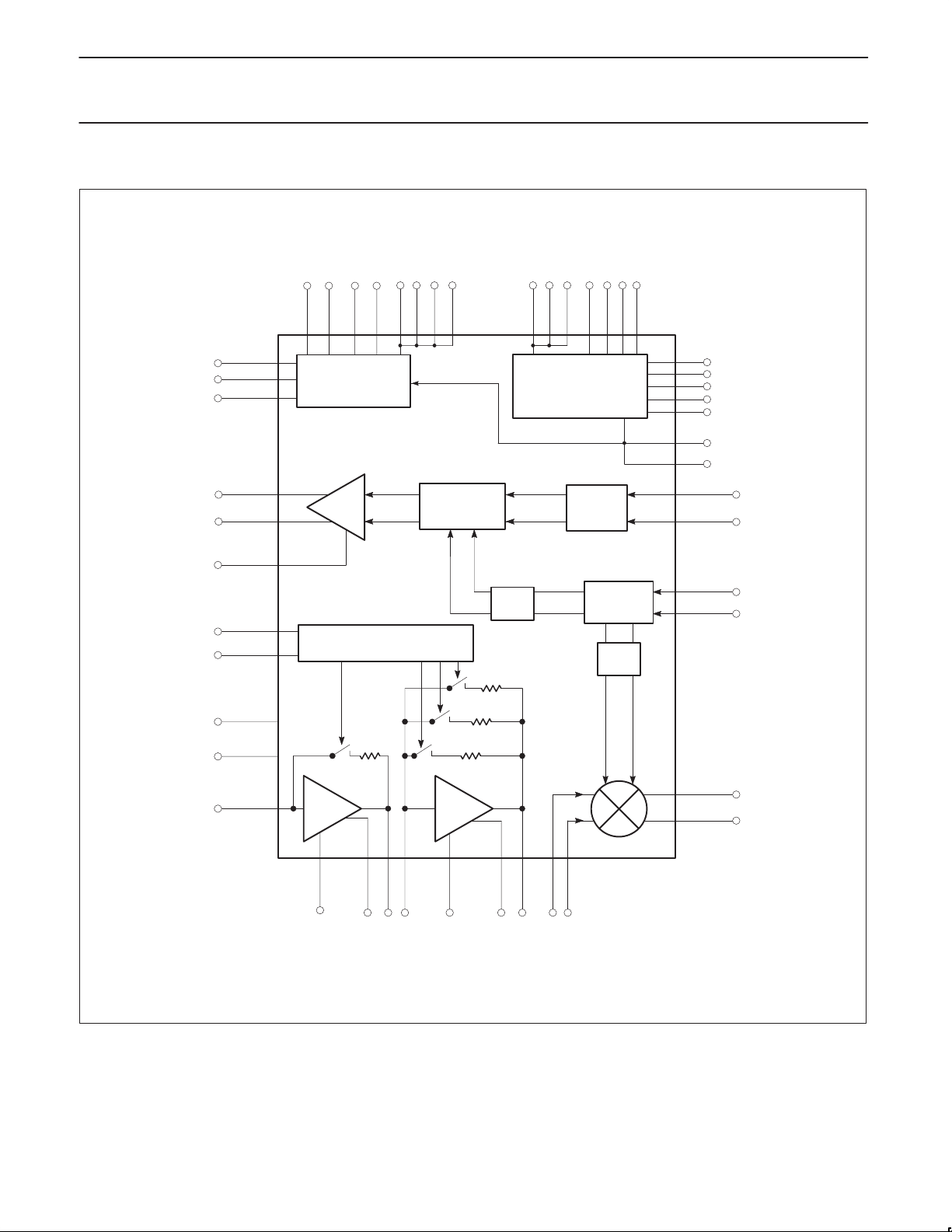
BLOCK DIAGRAM
BM
COMP1
COMP2
VCCGNDBM
GNDTx2
GNDTx1
GNDTx3
GNDTx4
GND1
GND2
GND3
PON
BATT
V
CON1
CON2
PDTx
PONRx
PONBUF
TxOX
RETx
VCCL1
VCCL2
TxO
IN1
TxIF
TxIFX
LO IN
LO INX
RxIF
RxIFX
VREG2
VREG2F2
GNDREG2
GNDREG1
VREG1
VCCTx1
VCCTx2
BANDGAP
BIAS SUPPLIES
SINGLE
SIDEBAND
MIXER
A
B
LNA1
ATTENUATION
CONTROL LOGIC
LNA2
VOLTAGE REGULATORS
TLO
BUFFER
TLOX
LINEAR
IF LEVEL
CONTROL
LO INPUT
BUFFER
BUFFER
RLO
RLOX
1997 May 22
GNDL1
OUT1
IN2
GNDL1A
GNDL2
Figure 2. Block Diagram
INM
OUT2
GNDL2A
INMX
SR00129
3
Page 4
Philips Semiconductors Product specification
SA1620Low voltage GSM front-end transceiver
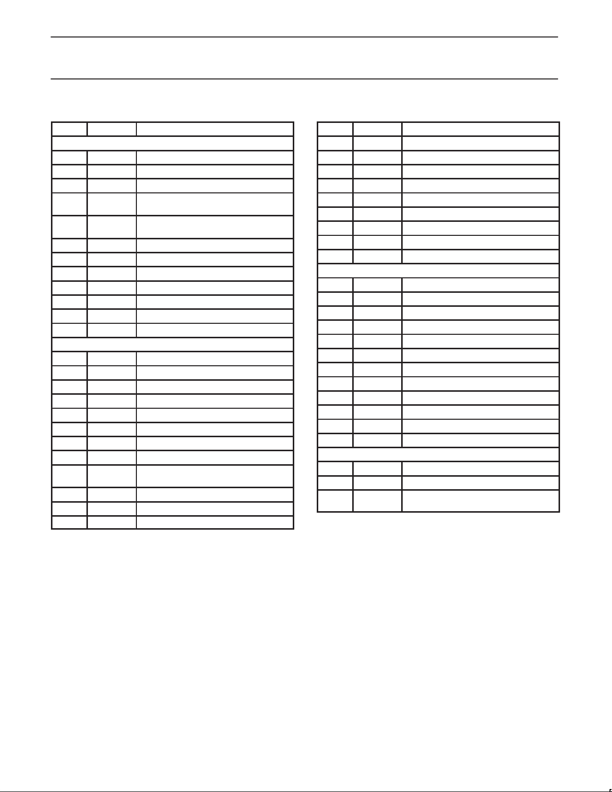
PIN DESCRIPTIONS
Pin No. Pin Name Description
DC Regulators
15 GND1 Ground of regulator supply
18 GND2 Ground of regulator supply
21 GND3 Ground of regulator supply
26 CON2 Control 2, voltage select for regulator 1
29 CON1 Control 1, voltage select for regulator 1
30 GNDREG2 Ground of regulator 2
31 VREG2 Output of regulator 2
32 VREG2F2 Feedback of regulator 2
33 VREG1 Output of regulator 1
34 GNDREG1 Ground of regulator 1
35 PON Power-on input of regulators
36 V
Rx Path
10 COMP2 Capacitor for bias stabilization
11 COMP1 Capacitor for bias stabilization
12 VCCBM VCC for Rx Bias and Rx mixer
NOTES:
1. Device is ESD sensitive. There are no ESD protection diodes at Pins 16, 17, 40 and 41. Thus, open-collector outputs may have increased
DC voltage or higher AC peak voltage.
2. Pins 15, 18 and 21 are connected to each other and to a separate ground in REG1 and REG2.
3. Pins 23, 25, 42 and 39 are connected to each other and to the Tx path, LO buffer and associated bias supplies.
4. Pins 22 and 24 are connected to each other providing a sense input. They are also connected to the Tx path, LO buffer and associated bias
supplies.
5. Pins 30 and 34 are not internally connected. They must be connected to external grounds.
6. Pins 48, 1, and 12 are not internally connected and have no ESD protection diodes between them. Power may be saved by connecting
V
BATT
1 VCCL2 Positive supply for LNA2
2 IN2 Input LNA2
3 GNDL2 Ground L2 for LNA2
4 GNDL2A Ground L2A for LNA2
5 OUT2 Output LNA2
6 B Attenuation select B for LNA1 and LNA2
7 A Attenuation select A for LNA1 and LNA2
8 INM RF input for Rx mixer, open emitter
9 INMX Inverse RF input for Rx mixer, open
L1 and IN1 or VCCL2 and IN2 to ground if LNA1 or LNA2 is not needed.
CC
and 2
and 2
Input of regulator 1 and 2
emitter
Pin No. Pin Name Description
13 GNDBM Ground for Rx Bias and Rx mixer
14 PONRx Power on input for Rx bias supply
16 RxIF IF output, open collector
17 RxIFX Inverse IF output, open collector
44 IN1 Input to LNA1
45 GNDL1 Ground L1 for LNA1
46 GNDL1A Ground L1A for LNA1
47 OUT1 Output LNA1
48 VCCL1 Positive supply for LNA1
Tx Path
19 TxIF IF input for Tx
20 TxIFX Inverse IF input for Tx
22 VCCTx1 Positive supply for Tx input
23 GNDTx1 Ground for Tx input
24 VCCTx2 Positive supply for LO and Tx input
25 GNDTx2 Ground for LO and Tx input
38 PDTx Power down Tx input
39 GNDTx4 Ground for Tx output
40 TxOX Inverse Tx output, open collector
41 TxO Tx output, open collector
42 GNDTx3 Ground 1 for Tx output side
43 RETx Reference resistor for Tx output current
Elements for Tx and Rx Path
27 LO IN Input for Local Oscillator signal
28 LO INX Inverse input for LO or AC ground
37 PONBUF Power on first stage LO input buffer and
bias
1997 May 22
4
Page 5

Philips Semiconductors Product specification
SA1620Low voltage GSM front-end transceiver
ABSOLUTE MAXIMUM RATINGS
SYMBOL PARAMETER RATING UNITS
V
CCXX
V
BATT
V
IN
∆V VCCTx1,2 pins to VCCBM -0.3 to +1 V
∆VG Any GND pin to any other GND pin 0 V
P
D
T
JMAX
P
MAX
T
STG
V
, V
TXO
TXOX
V
, V
RXIF
RXIFX
NOTE:
1. Maximum junction temperature is determined by the power dissipation is determined by the operating ambient temperature and the thermal
resistance, θ
Supply voltages -0.3 to +6.0 V
Battery voltage -0.3 to +8.0 V
Voltage applied to any other pin -0.3 to (V
+0.3) V
CCXX
Power dissipation, TA = 25°C (still air) 800 mW
Maximum operating junction temperature 150 °C
Maximum power input/output +20 dBm
Storage temperature range –65 to +150 °C
Positive RF peak voltage at Tx outputs 6 V
Positive IF peak voltage at Rx mixer outputs 6 V
. 48-pin TQFP: θJA = 67°C/W.
JA
DC REGULA TORS
Two low drop regulators (REG1 and REG2) are included on the chip
and may be used to deliver the supply voltage of the main circuitry
(e.g., 3V) out of the battery (at V
Figure 4 and in Table 1.
REG1 is intended to supply, at least, the internal functions of the
SA1620. Both regulators may also be used for external circuitry.
For this application, different voltages may be programmed as
shown in Table 1.
The transmitter supply pins (V
connection in the feedback loop of REG1 and must be externally
connected to pin VREG1. For REG2, the sensor pin VREGF2 must
be connected to VREG2.
All ground pins are internally bonded to the header except for pins
GNDL1, GNDREG1 and GNDREG2.
When both regulators are not used, connect pins V
CON1, CON2, VREG1, VREG2 and VREG2F2 to ground.
= 3.3 to 7.5V) as shown in
BATT
Tx1,2) also operate as a sensor
CC
, PON,
BATT
Table 1. DC Reg Output Voltage Control Pins
CON1 CON2 VREG1 VREG2 UNITS
L L 3 ± 5% 3 ± 5% V
L H 3.4 ± 5% 3.4 ± 5% V
H L 3.7 ± 5% 3.7 ± 5% V
H H 5.1 ± 5% 5.1 ± 10% V
NOTES:
1. Logic levels at CON1 and CON2:
H – Open circuit. Pin must not be connected externally.
Logic high level supplied on chip.
L – Connected to ground.
2. Currents at CON1 and CON2:
H – 0µA
L (PON = H) – 50µA
L (PON = L) – <1µA
1997 May 22
5
Page 6

Philips Semiconductors Product specification
SYMBOL
PARAMETER
UNITS
6
F
7
f
dB
SA1620Low voltage GSM front-end transceiver
Table 2. DC Regulators
and V
LIMITS
VREG1
VREG2
REG2
/10 mA
/10 mA
at V
BATT
= 3.3V,
kHz
TEST
V
BATT
VREG1,
VREG2
I
INT1
I
INT2
I
, I
INT01
I
VREG1MAX
I
VREG2MAX
BW
CONDITIONS
Common positive input voltage at both regulators VREG1+0.3 V
Output voltages of regulators 1 and 2 V
= 3.3V 2.85 3 3.15 V
BATT
Internal current of REG1 in power-on mode 4 + I
Internal current of REG2 in power-on mode 2.5 + I
Internal current in power-down mode <15 µA
INT02
5
Max output current at VREG1 100 mA
5
Max output current at VREG2 30 mA
V
V
V
BATT
BATT
BATT
= 3.3V, I
= 3.3V, I
= 7.5V, I
= 0.1mA 0.03
REG1
= 100mA 60
REG1
= 100mA 80
REG1
MIN TYP MAX
≤100kHz ≤–61
10MHz ≤–32
REG
100MHz ≤–37
400MHz ≤–48
NOTES:
1. Power-on pin of Regulator 1 and 2: PON
2. Input currents at PON: <1µA. There are no pull-up or pull-down resistors.
3. Feedthrough attenuation from the logic input PON to the outputs VREG1 and VREG2: ≥40dB.
4. Recommended load capacitors: C529 = C530 = 1µF to ground with series resistance ≤0.1Ω. See Figure 4. Additional optional capacitor
≤1000µF with series resistance ≤5Ω.
≥ 150°C a thermal switch reduces the output current.
5. At T
j
6. Typical open loop bandwidths of regulator 1 at V
7. Feedthrough attenuation (at the indicated frequency f) from the input V
(CON1=CON2=L)
= 3V and C529 = 1µF.
REG1
to the outputs V
BATT
REG1
1997 May 22
6
Page 7
Philips Semiconductors Product specification
SYMBOL
PARAMETER
TEST CONDITIONS
UNITS
VR1Internal supply at pin RET
V
IR1Current at pin RET
mA
SA1620Low voltage GSM front-end transceiver
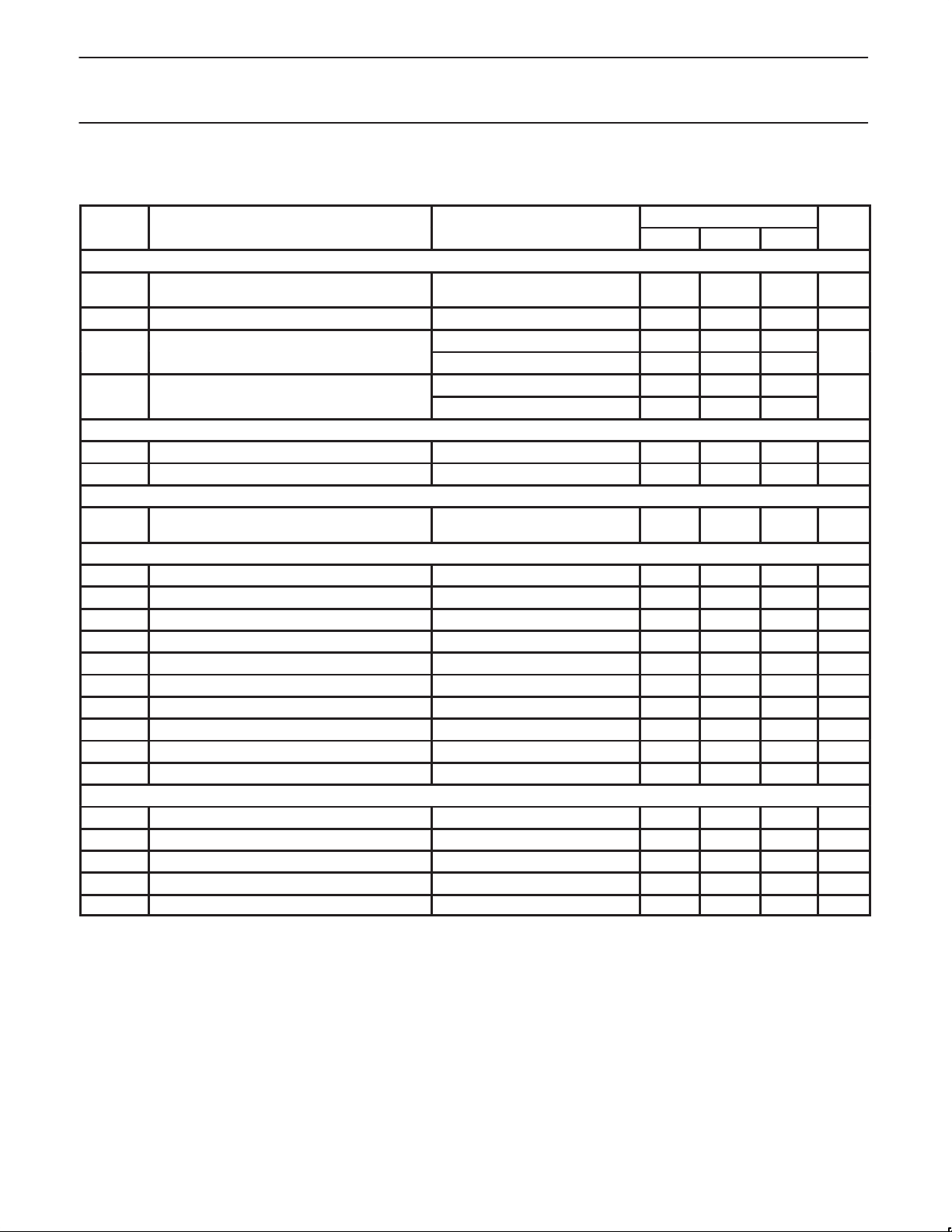
DC ELECTRICAL CHARACTERISTICS
V
= +3V, TA = 25°C; unless otherwise stated.
CCxxx
LIMITS
MIN TYP MAX
Transmitter
I
VCC
R1 External resistor
Total supply current
1
pp
p
p
x
x
Low noise amplifiers
I
L1 Current at pin VCCL1 G1hi mode 2.5 3.5 5 mA
VCC
I
L2 Current at pin VCCL2 G2hi mode 2.5 3.5 5 mA
VCC
Receiver
I
VCC
Total supply current
Regulators
Vreg1 Voltage @ 100mA load Con1 Con2
L L 2.85 3.0 3.15 V
L H 3.23 3.4 3.57 V
H L 3.515 3.7 3.885 V
H H 4.61 5.1 5.61 V
Vreg2 Voltage @ 30mA load Con1 Con2
L L 2.85 3.0 3.15 V
L H 3.23 3.4 3.57 V
H L 3.515 3.7 3.885 V
H H 4.61 5.1 5.61 V
Logic levels
V
V
V
I
C
2
Logic 1 level PONBUF, PDTx, PONRx, A, B 2.0 V
IH
Logic 1 level P
IH
Logic 0 level 0 0.8 V
IL
Input logic current 1 µA
I
Input logic capacitance 1.7 pF
Ia
NOTES:
+ I
1. The output current I
2. Thresholds are independent of supply voltages. Thus the SA1620 is compatible with SA1638 and with the power down inputs of usual
TXO
is adjustable by the external resistor R546. I
TXOX
external voltage regulators.
3. P
ON
logic 1 max is V
BATT
.
Transmit mode
= 240Ω
R
546
59 90 mA
240 Ω
VCCTx1,2 = 2.7V 0.43
VCCTx1,2 = 5.5V 0.45
R546 = 240Ω, VCCTx1,2 = 2.7V 1.7
R546 = 240Ω, VCCTx1,2 = 5.5V 1.8
Receive mode
= 240Ω
R
546
ON
+ I
TXO
TXOX
= 10 * I
2.0 V
, I
R546
R546
28 39 mA
= VR1/R546,
CCBM
BATT
3
V
V
1997 May 22
7
Page 8
Philips Semiconductors Product specification
SYMBOL
PARAMETER
TEST CONDITIONS
UNITS
S
dB
∆S21/∆T
Gain temperature sensitivit
dB/°C
S
dB
∆S21/∆T
Gain temperature sensitivit
dB/°C
SA1620Low voltage GSM front-end transceiver
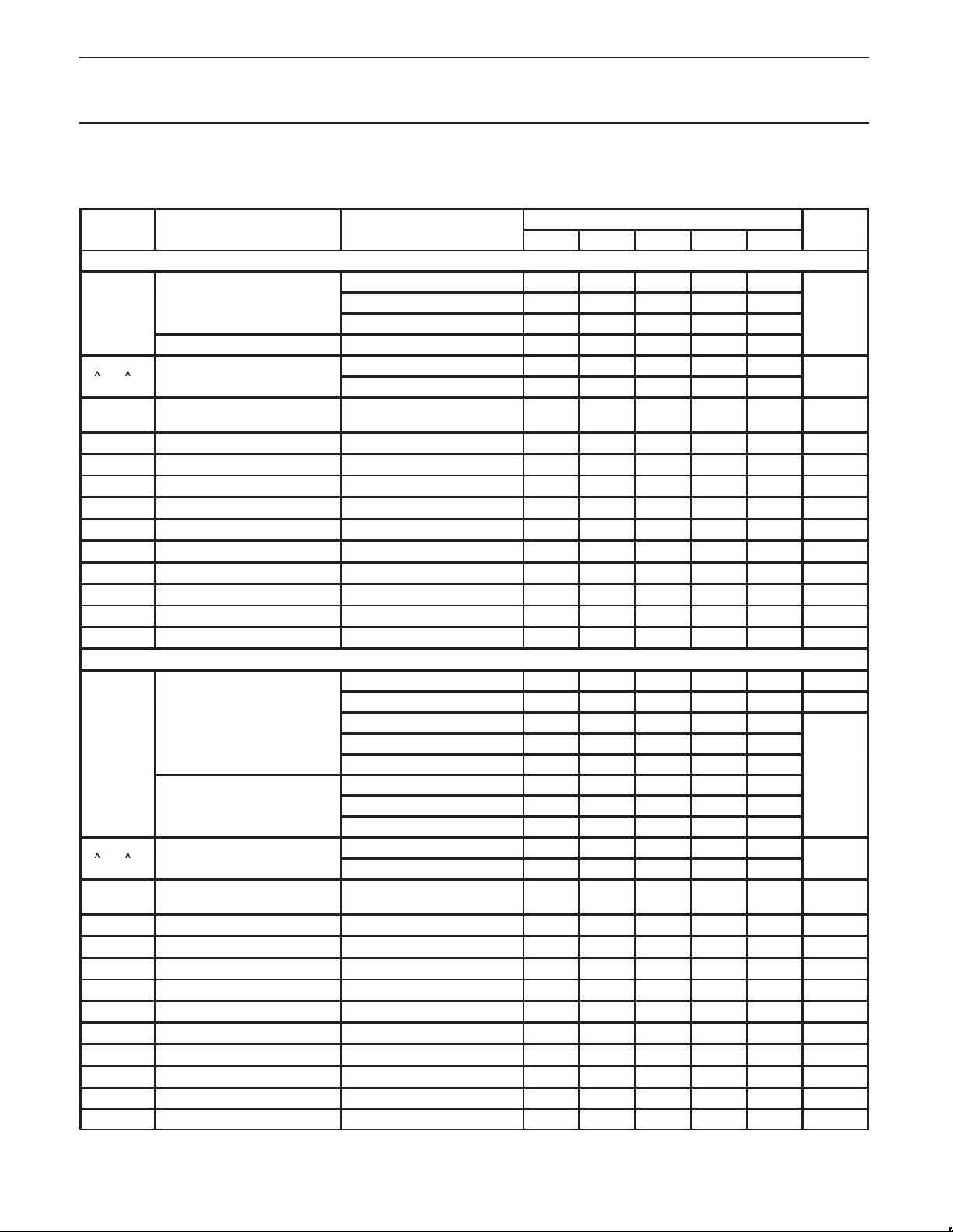
AC ELECTRICAL CHARACTERISTICS
V
= +3V, TA = 25°C; RF = 940MHZ; IF=400MHz, fLO=RF + IF; LO = –15dBm; unless otherwise stated.
CCXX
1
LIMITS
1
Low Noise Amplifier LNA1
MIN
2
-3σ TYP 3σ MAX
G1hi mode 9.4 10 10.6
Gain
21
G1hi mode, RF = 1800MHz –2.5
G1lo mode –13 –12 –11
IP3 G1lo mode 28
G1hi mode 0.003
G1lo mode 0.0140
∆S21/
∆V
CCL1
p
y
Gain/voltage sensitivity 0.1 dB/V
∆S21/∆f Gain frequency variation 0.01 dB/MHz
S
S
S
P
-1dB
Reverse isolation G1hi mode –19 dB
12
11
22
Input match
Output match
3
3
50Ω –11 dB
50Ω –14 dB
Input 1dB gain compression G1hi mode –15.5 –14 –12.5 dBm
IIP3 Input third order intercept –5.5 –4 –2.5 dBm
IIP3/∆t Input third order intercept 0.011 dB/°C
NF Noise figure 1.9 dB
t
ON
t
OFF
Low Noise Amplifier LNA2
Turn-on time 7 µs
Turn-off time 0.5 µs
2
G2hi mode 9 10 11 dB
G2hi mode, RF = 1800MHz –1.5 dB
Gain
G2lo1 mode –8.5 –7.5 –6.5
G2lo2 mode –22.5 –21.5 –20.5
21
G2lo3 mode –30 –28.5 –27
G2lo1 mode 18
IP3
G2lo2 mode 20
G2lo3 mode 25
G2hi mode 0.003
G2lo1,2,3 modes 0.014
∆S21/
∆V
CCL2
p
y
Gain/voltage sensitivity 0.1 dB/V
∆S21/∆f Gain frequency variation 0.01 dB/MHz
S
S
S
P
-1dB
Reverse isolation G2hi mode –24 dB
12
11
22
Input match
Output match
3
3
50Ω –13 dB
50Ω –15 dB
Input 1dB gain compression G2hi mode –18 –16 –14 dBm
IIP3 Input third order intercept –8 –6 –4 dBm
IIP3/∆t Input third order intercept 0.019 dB/°C
NF Noise figure 2 dB
t
t
ON
OFF
Turn-on time 7 µs
Turn-off time 0.5 µs
1
°
°
1997 May 22
8
Page 9
Philips Semiconductors Product specification
SYMBOL
PARAMETER
TEST CONDITIONS
UNITS
PG
Power conversion gain
5
dB
SA1620Low voltage GSM front-end transceiver
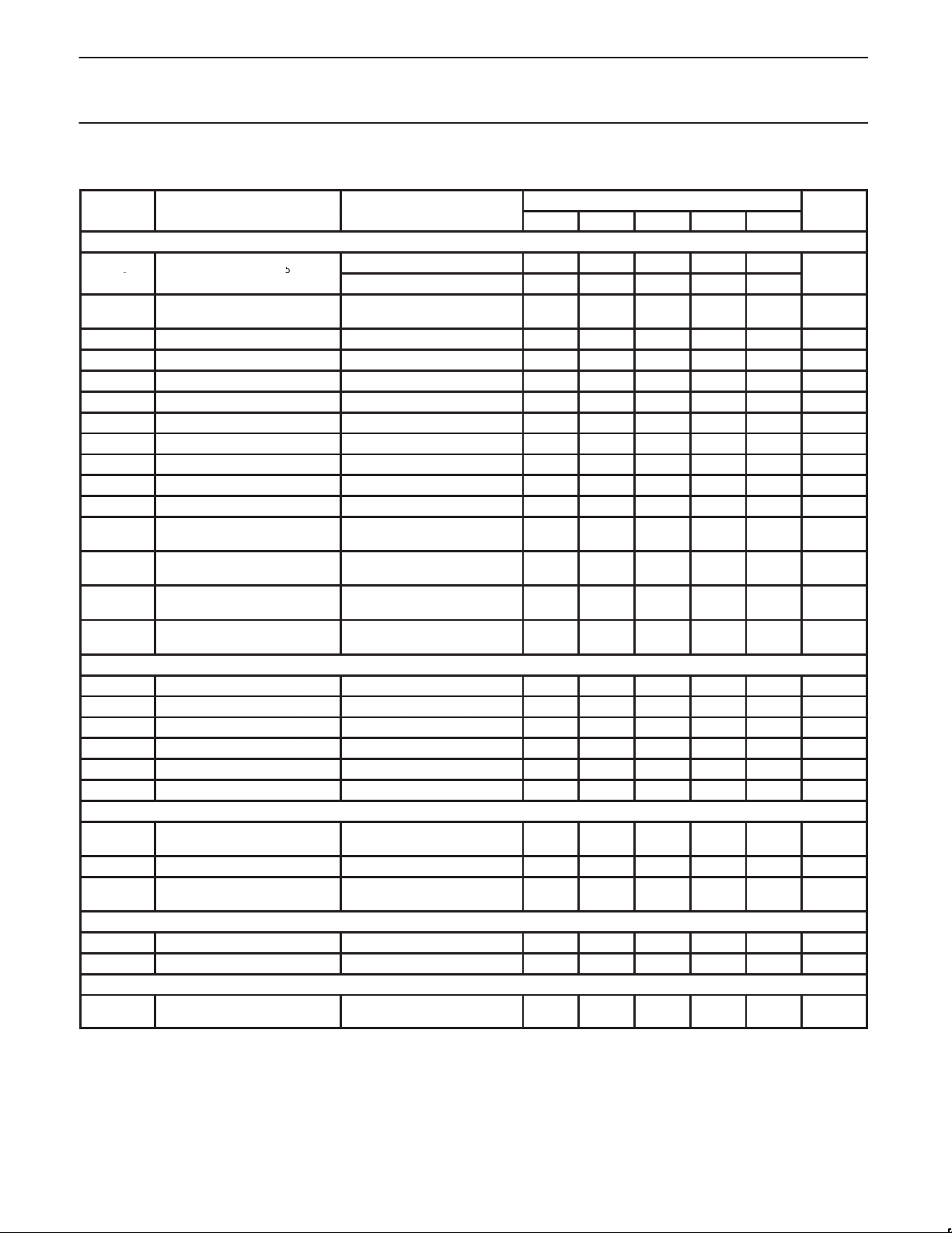
AC ELECTRICAL CHARACTERISTICS (continued)
1
LIMITS
1
MIN
-3σ TYP 3σ MAX
Rx Mixer
7.5 +8.5 9.5
P
S
NF
11
-1dB
C
Mixer input match at ports INM
and INMX
SSB combined noise figure 10 dB
M
4
Input 1dB compression –7.3 dBm
RF = 1800MHz –4
–13 dB
IIP3 Input third order intercept 0 2 4 dBm
IIP3/∆t Input third order intercept 0.005 dB/°C
IIP2 Input second order intercept 19 dBm
G
RFM-IF
G
LOfloor
G
LO-IF
G
LO-RFM
G
LO-RF1
G
LNA1-2
G
LNA2-M
G
LNA1-M
Receiver
RF feedthrough 400MHz –26 dB
LO floor feedthrough 400MHz –30 dB
LO feedthrough to IF 1.3GHz –16 dB
LO to mixer input feedthrough 1.3GHz –50 dBm
LO to RF LNA1 input
feedthrough
LNA1 output to LNA2 input
feedthrough
LNA2 output to mixer input
feedthrough
LNA1 output to mixer input
feedthrough
6
1.3GHz –65 dBm
400MHz
1290-1760MHz
–41
–26
1290-1760MHz –23 dB
400MHz
1290-1760MHz
–50
–35
Cascaded gain A,B Logic Level
H,H 23.5 26.5 28.5 30.5 33.5 dB
H,L 6 9 11 13 16 dB
L,H –8 –5 –3 –1 +2 dB
L,L –41 –36 –32 +28 –23 dB
Input IP3 @ RFin=–40dBm H,H –20 –18 –16 dBm
LO input
Z
P
A
SAT
Input impedance
IN
(each single-ended input)
Input power –25
IN
1.3GHz 35-j97 Ω
Transistor saturation limit,
max input amplitude
7
–15 dBm
500 mV
Tx IF input
|ZIN| Input impedance 400MHz 2 kΩ
P
Input power –20 dBm
IN
Tx RF output
P
OUT
R546 = 240Ω,
Tx1,2 = 3V
V
CC
5 7.5 8.5 9.5 dBm
NOTES:
1. Due to our automatic test equipment accuracy and repeatability test limits may not reflect the ultimate device performance. Standard
deviations are calculated from characterization data.
2. If the LNA1 is not needed, connect pin V
3. Simple L/C elements are needed to achieve specified return loss.
L1 and IN1 to GND. If the LNA2 is not needed, connect pin VCCL2 and IN2 to GND.
CC
4. The mixer RF inputs (emitters of a Gilbert Cell) may be driven by a symmetrical matching network.
5. Input symmetry suppression is such that the product 6*RF–4*LO is to be suppressed by at least 66dB relative to the wanted IF output when
the input to the mixer is at –32dBm.
6. LNA1, LNA2, and the mixer are cascaded. 0 db insertion loss between LNA1 out to LNA2 in and LNA2 out to mixer in.
7. Lowering the LO input power (P
) from TYP to MIN will lower the mixer gain (PGC) by 1 dB.
IN
1
dB
dB
1997 May 22
9
Page 10
Philips Semiconductors Product specification
SA1620Low voltage GSM front-end transceiver
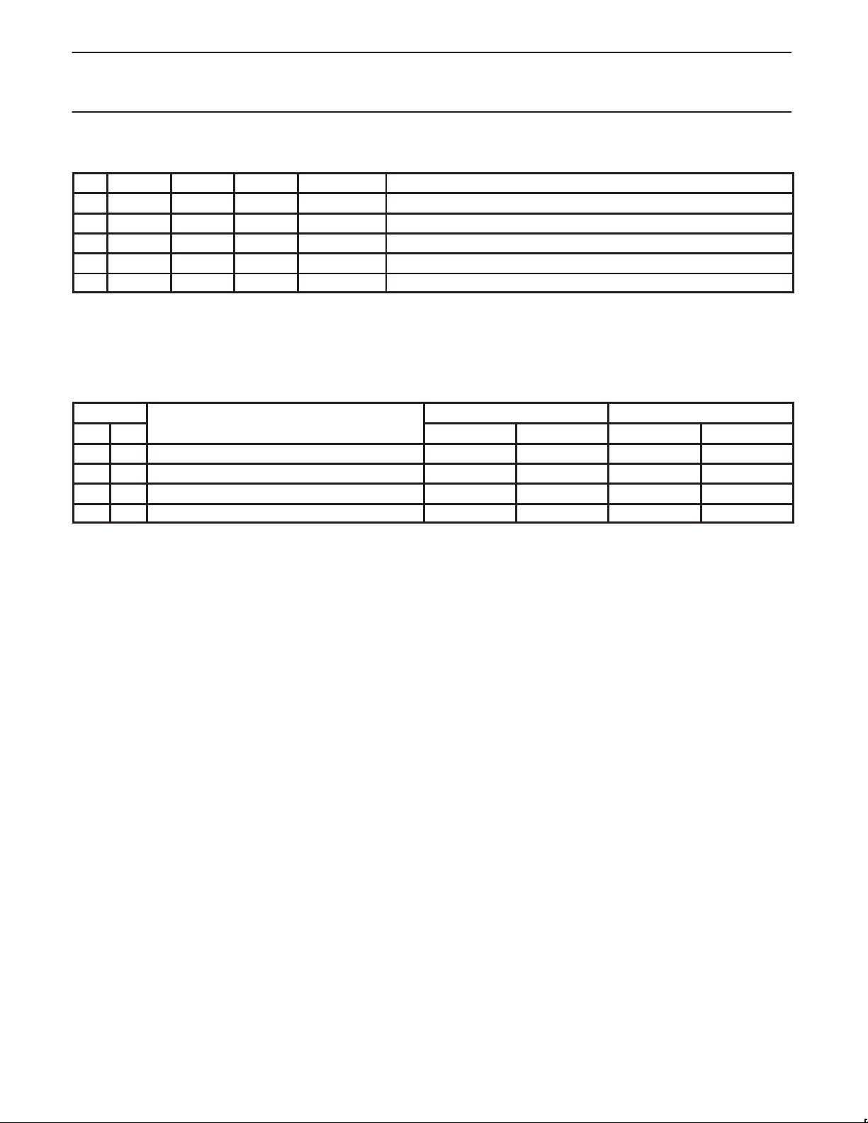
Table 3. Power-Down and Tx/Rx Control Logic
No. PONBUF PDTX PONRX MODE RESULT
1 H H L Standby LO buffer active, Tx and Rx path inactive
2 H L L Transmit LO buffer active, Tx path active, Rx path inactive (LNAs + mixer)
3 H H H Receive Tx path inactive, LO buffer and Rx path active (LNAs + mixer)
4 H L H Calibrate Tx path and Rx LNAs inactive, LO buffer and Rx mixer active
5 L x x Power-Down Tx- and Rx-path, LO buffers and Bias inactive
NOTES:
1. Logic levels of PONBUF, PDTx and PONRx: TTL, see DC Electrical Characteristics.
2. Logic levels / polarities are compatible with Philips Semiconductors Power Amp Controller PCA5075 and synthesizers UMA1019 or SA8025.
3. First stage of LO buffer and parts of bias supply are powered on by PONBUF .
4. Tx- or Rx-paths may be activated for special timeslots. Lines 1 and 4 show options to support DC offset calibrations at baseband mixers,
following in the receiver chain (SA1638).
Table 4. Gain Control Logic for LNA1 and LNA2
INPUT
a b
H H 0 G1hi G2hi on on
H L 1 G1hi G2lo1 on off
L H 2 G1hi G2lo2 on off
L L 3 G1lo G2lo3 off off
NOTES:
1. Logic levels of a and b: TTL
2. For values of G1hi and G1lo, G2hi, G2lo1, G2lo2 and G2lo3 see LNA1 and LNA2 AC Electrical Characteristics.
ATTENUATION
STEP
LNA1 LNA2 LNA1 LNA2
GAIN POWER CONSUMPTION
1997 May 22
10
Page 11
Philips Semiconductors Product specification
SA1620Low voltage GSM front-end transceiver
I
I
I
Q
I
Q
Q
Q
BOUT
(to SA1620 ATTENUATION
CONTROL LOGIC INPUTS)
AOUT
SA1638
400MHz
LINEAR
IF LEVEL
CONTROL
400MHz
LO1
(1290–1360MHz)
BUFFER
LO2
800MHz
SAW
÷
÷
PD
÷
CLKIN
13MHz
(SA8025, UMA1019)
FREQUENCY SYNTHESIZER
INTERFACE TO
MICROCONTROLLER
1997 May 22
INTERFACE TO
MICROCONTROLLER
SA1620
INPUT
SERIAL
PCA5075
POWER AMP
CONTROLLER
SSB
PA
MIXER
Tx/Rx
POWER
SUPPLY
ATTENUATION
A
Tx:
935–960MHz
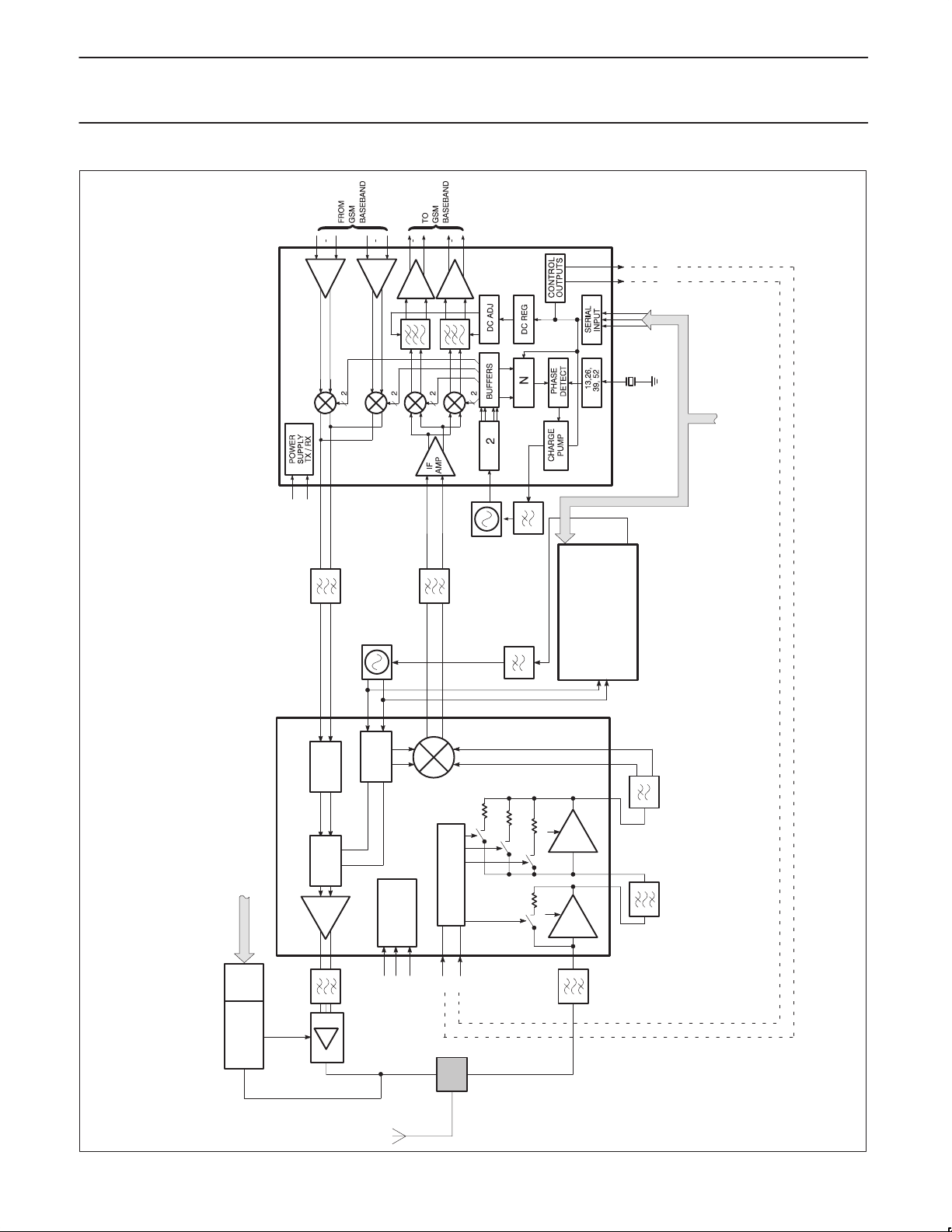
Figure 3.
CONTROL LOGIC
B
Rx:
11
890–915MHz
PD
LNA1 LNA2
SR00130
Page 12

Philips Semiconductors Product specification
SA1620Low voltage GSM front-end transceiver
Overview of Dual GSM/PCN Architecture
The SA1620 RF front-end and SA1638 IF transceivers form a dual
conversion architecture which uses a common IF and standard I/Q
baseband interface for both transmit and receive paths. This
approach avoids the screening difficulties of direct modulation in the
transmit direction and the mass production and practical
performance issues related to direct conversion in the receive
direction. The time division multiplex nature of the GSM system
permits integration of the transmit and receive functions together on
the one RF and one IF chips. This simplifies the distribution of local
oscillator signals, maximizes circuitry commonality, and reduces
power consumption.
The SA1620 and SA1638 allow considerable flexibility to optimize
the transceiver design for particular price/size/performance
requirements, through choice of appropriate RF and IF filters. The
receive IF may be chosen freely in the range 70–500MHz, while the
transmit IF is fixed to 400 MHz. The comparison frequency of the
SA1638 PLL is high in order to provide fast switching time.
With suitable choice of the IF, an identical SA1638 IF receiver
design can be used for both 900MHz GSM and 1800MHz PCN
(DCS1800) equipment.
General Benefits/Advantages
•2.7V operation. Compatible with 3V digital technology and
portable applications. (Higher voltage operation also possible, if
desired.)
•Excellent dynamic range. The availability of two LNAs allows
flexibility in receiver dynamic design for portable and mobile GSM
spec. applications with appropriate filters. If for a particular
application a GaAs or discrete front-end is desired, one of the
LNAs can be left unpowered. The placing of the AGC gains
switches at the front means that for most of the time some
attenuation will be inserted, further increasing typical dynamic
performance beyond that specified by GSM.
•High power transmit output driver, delivering +8.5dBm output.
This is sufficient to drive a filter and power amplifier input, without
a driver amplifier. To avoid unnecessary current consumption the
output power can be reduced, if not required, by appropriate
choice of an external resistor.
•DC offsets generated in the receive channel are independent of
the AGC setting, and correctable by software to prevent erosion of
signal handling dynamic range by DC offsets. Independence of
DC from AGC setting is achieved by putting the gain switches in
the RF front-end.
•Minimal high-quality filter requirements. As a result of the
integration in the SA1638 of high quality channel selectivity filters,
only sufficient filtering is needed in the receive path to provide
blocking protection for the second mixers. This reduces receiver
cost and size.
•Operation at a high IF allows RF image reject filters to be relaxed.
For example, at a 400MHz IF, the natural gain roll-off in the LNAs
and mixer suppresses the image signal in the 1800MHz band by
typically 28dB below the desired 900MHz band signal.
Receive Path
Multiple LNAs allow the flexibility to exploit the best choice of
currently available filters (on performance, size, or cost grounds).
This approach is preferable to a single high-gain stage as the stray
cross-coupling effects between pins remain manageable. In a single
stage amplifier this would limit the amount of rejection of out-of-band
signals that could be achieved, and would also limit the amount of
AGC attenuation that could be practically implemented.
The LNAs are powered up only when PONBUF, PDTx and PONRx
are high, to allow a high degree of battery economy. If greater
sensitivity is required for an application, an external preamplifier
circuit can be used instead of LNA1, and LNA1 left unconnected.
A special mode is provided with just the IF output related circuitry
active in order to allow calibration of the DC offset at the SA1638
baseband receive outputs. This offset contains a contribution due to
coupling effects between the second local oscillator and the IF
circuitry, and therefore the receiver is set up in the receive state (but
with incoming signals excluded) to allow accurate offset calibration.
Gain Control
Gain control is implemented in the SA1620 RF front-end. This
avoids the disruption of the DC offset at the baseband IQ outputs
that is typically caused by changes in the AGC. The SA1620 and
SA1638 are designed so that the GSM dynamic range requirements
can be met with the AGC remaining on the maximum gain setting.
These gain steps scale the dynamic range of the received signal
(e.g., 90dB for GSM) into the dynamic range of the baseband
processing device.
The absolute gain tolerances may be measured together with the
attenuation tolerances of external filters during production of the
receiver equipment. After software calibration switching from one
dynamic range to another will cause only minor errors.
Tx Path
TXIF and TXIFX are differential IF inputs for phase modulated
signals (e.g., GMSK). There is an IF level control loop which
provides a constant amplitude to an image reject up mixer. Thus,
this mixer operates linearly in the IF path, independent of IF level
tolerances.
The single sideband up mixer is sufficient in quadrature to achieve
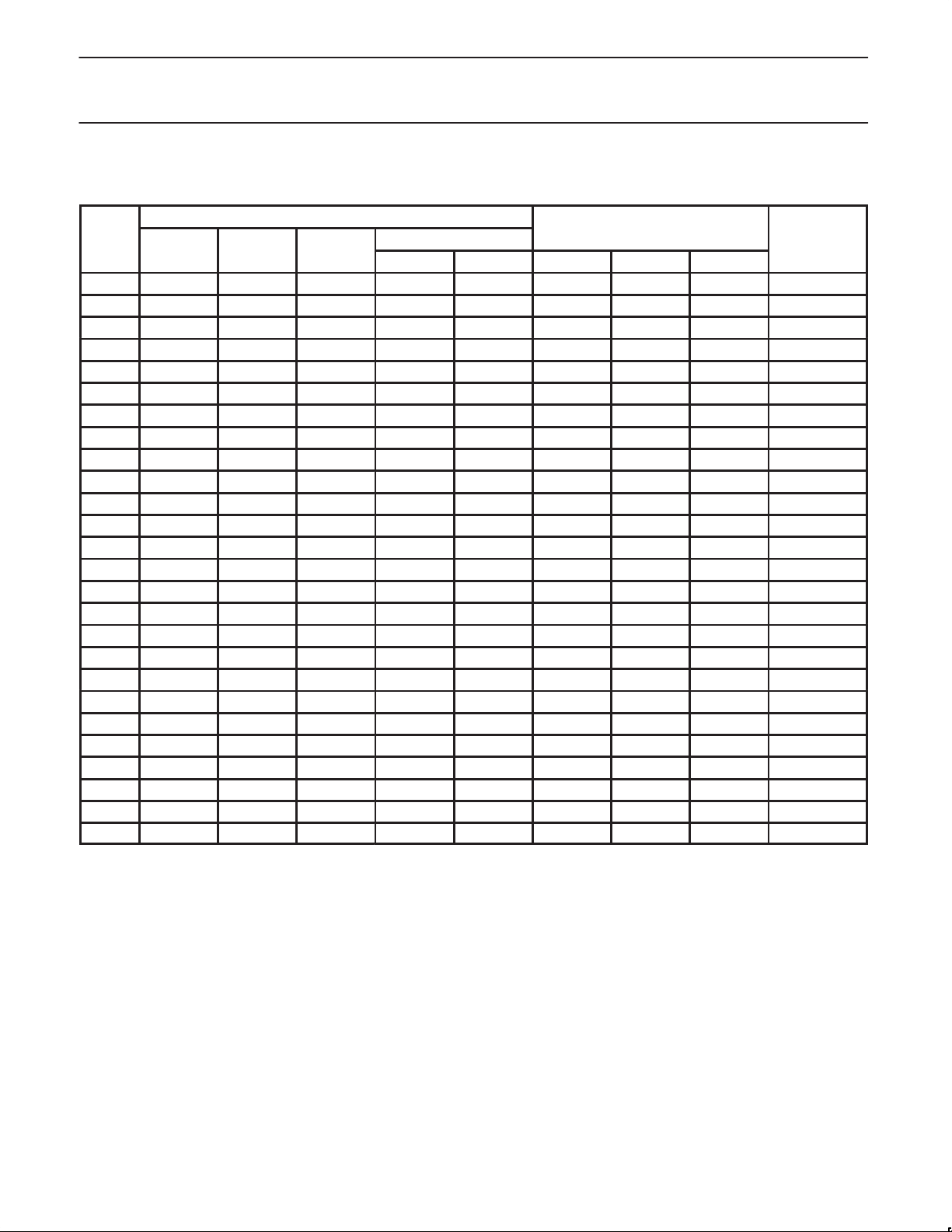
the typical performance indicated in Table 6 over an IF range of 250
to 500MHz. The mixer is operating in switching mode by well
matched 0° and 90° LO signals, optimized for 1.1 to 1.5GHz.
The Tx output stage operates in switching mode. Thus, parasitic
AM at the IF is not transferred. The outputs TXO and TXOX may be
used symmetrically or single-ended. Some spurious emissions will
be very low when a symmetrical output signal is used.
=
R
e
6.25V (Z
OUT
Z
Pin 40
I
R546
is adjustable with R546 and is accurate to
Pin 41
V
R
) (I
R546
546
P
OUT
according to Figure 4 and
Characteristics. P
within ±1dB over the full voltage range 2.7 to 5.5V, and ±0.5dB from
a given supply voltage. The absolute limit of the negative peak
voltage swing at pins TxO and TxOX is V
absolute limit of the positive peak voltage is +6V .
2
)
R546
according to DC Electrical
= VCCTx1,2 – 1V. The
SAT
1997 May 22
12
Page 13
Philips Semiconductors Product specification
SA1620Low voltage GSM front-end transceiver
L612
I=56n
C610
c=3.9p
LNA_In
c=33p
C611
TMXR_Out
C613
o
690
C575
c=33p
V503
c=33p
C609
C573
r=100
C574
c=33p
Vbatt
vdc=7.5
– +
c=3.9p
c:1p
R651
C635
Vcc/Gnd
Vcc/Gnd
335
335
R546
r=240
940
C650
c=33p
605
c–100n
C527
c=100n
PDTx
TxOX
TxO
RETx
IN1
OUT1
VccL1
c=10u
PONBUF
GNDTx4
GNDTx3
GNDL1
GNDL1A
C636
VBATT
VCCL2
C528
c=100n
Vbatt/Gnd
PON
IN2
Vcc
VREG1
GNDREG1
GNDL2
GNDL2AAOUT2
Open/Gnd
CON1
LO_In
C564
c=33p
C565
LOINX
C=33p
LOIN
Open/Gnd
CON2
GNDTx2
8/12/96
VRegF2
c=1u
C530
(ceramic!!!)
C=1u
C529
(ceramic!!!)
VREG2
VREGF2
GNDREG2
10 mils wide, xxx mils long on 31 mils
thick FR4 substrate.
SA 1620
xxx
B
INM
INMX
COMP1
COMP2
VCCBM
VccTx2
GNDTx1
VccTx1
GDN3
TxIFX
TxIF
GND2
RxIFX
RxIF
GND1
PONRx
GNDBM
C618
C615
350
350
c=8.2p
350
350
C622
gnd
c=10p
c=10p
C623
c=10p
Vcc/Gnd
c=33p
C539
L617 I=22n
o
o
TMXR_In
I=22n
L627
L624
o
C628
c=3.3p
C620
I=56n
c=100n
1997 May 22
LNA1_Out
C533
c=33p
C534
c=33p
c=1n
C339
890
L648
LNA2_In
I=56n
o
650
C336
LNA2_Out
Vcc/Gnd
c=33p
C644
RMXR_In
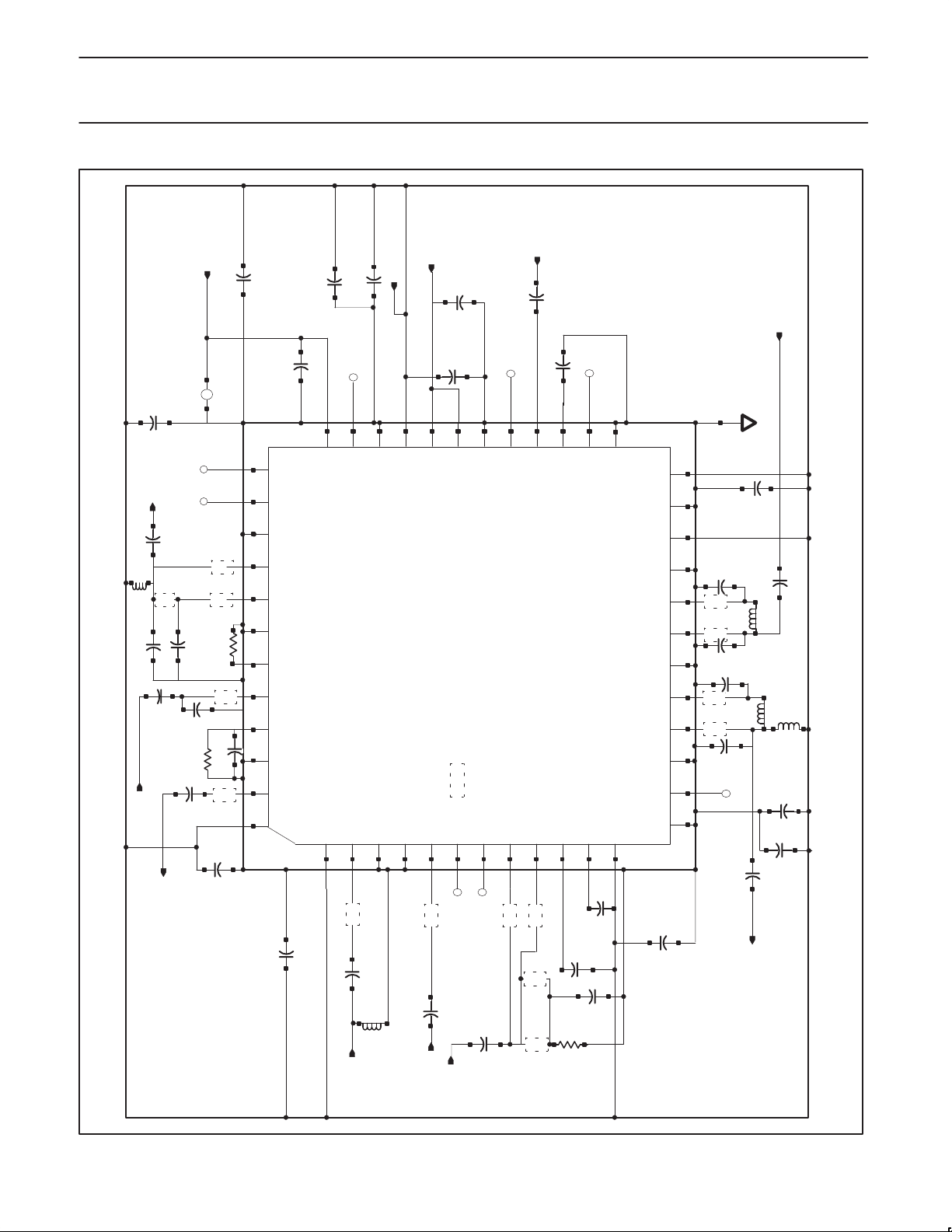
Figure 4. Application Circuit
13
340
Vcc/Gnd
c=33p
340
180
C631
c=4.7p
420
c=10n
R641
C380
r=100
C645
c=10n
C643
c=33p
C535
c=100n
C626 c=3.3p
RMXR+Out
C619
c=33p
SR01332
Page 14

Philips Semiconductors Product specification
SA1620Low voltage GSM front-end transceiver
APPLICATION CIRCUIT
LNA
Impedance Match: Intrinsic return losses at the input and output
ports are 7dB and 11dB, respectively. However, since long and
narrow traces are always needed to fan out the pins, the user can
adjust the traces’ dimensions so that only one shunt capacitor at the
input is required to achieve excellent impedance match for both
ports. If the user wants to skip the input matching network for
simplicity, then roughly 0.7dB gain would be lost, although it benefits
the system IP3.
Noise Match: The LNA1 and LNA2 can achieve 1.9dB and 2.0dB
noise figure, respectively, when S11 = –11dB. Further improvement
in S
will slightly decrease NF and increase S21.
11
Gain Control: The LNA1 can be switched to the attenuation mode,
while LNA2 has three attenuation modes to choose from. When
gain and loss modes from two LNAs are combined, there will be a
total dynamic range of 59dB in the RF block; 3.0V operation is
preferred to achieve better IP3 for both LNA1 and LNA2.
Temperature Compensation: Both LNAs have a built–in temperature
compensation scheme to reduce the gain drift rate to 0.003dB/°C
from –40°C to +85°C.
Supply Voltage Compensation: Unique circuitry provides gain
stabilization over wide supply voltage range. The gain changes no
more than 0.5dB when V
increases from 2.7V to 5.5V .
CC
Mixer
Mixer Input Match: The mixer is configured for best gain, noise
figure and spurious response. The user must supply an external,
patented resonant balun to provide the differential drive as well as
the impedance match (embedded in). Because the mixer consists
of two single–balance mixers, whose inputs are connected in
parallel instead of in series, the differential and common–mode
impedances are equal.
Output Match: The mixer output circuit also features an external,
patented resonant balun to optimize the conversion gain and noise
figure. The principal IF operating frequency is 400 MHz.
LO Drive: The internal buffer only requires –15dBm from an external
source. Furthermore, the transmitter incorporates an integrated
SSB upconverter that consists of narrowband phase shifters at
1300MHz (LO side) and 400MHz (IF side), so the LO frequency is
recommended to be the receiver band plus 400MHz. Additionally,
the LO leakage at the input of LNA1 is extremely low, which can
greatly alleviate the LO re–radiation problem.
Outband Blocking: For optimum performance, passive R/C network
is added at each input of the mixer. The resistors degenerate the
noise conversion gain, while the capacitors preserve the gain and
noise figure at RF frequencies.
Noise Figure and IP3: The resonant balun is superior to the
conventional balun in terms of insertion loss, size and cost. As a
result, the user can expect excellent SSB noise figure and gain
which is 10dB and 8.5dB, respectively, at 400MHz IF. And the
associated input IP3 is 2dBm typically. In the meantime, due to the
internal LO buffer, the noise figure and IP3 are not sensitive to the
LO levels. As discussed in the LNA Impedance Match session, a
better system IP3 can be achieved (if necessary) through LNAs’
gain reduction.
Transmitter
The resonant balun is applied again to maximize the gain and output
power, for a given bias current. Typical output power is 8.5dBm
when the input level exceeds –25dBm.
LO Input
The LO input is used in Tx- and in Rx-mode.
Only one synthesizer PLL is necessary to supply the LO input with
different frequencies in Tx and Rx timeslots.
The LO input buffer should only be set in power-down mode
together with the PLL. As further buffering is included on chip there
will be no influence on the PLL in active mode when the SA1620 Rxor Tx-path is power On or Off. Current consumption can thus be
saved by powering on the Rx- and Tx-circuitry just before it is
required, without disruption of the LO circuitry. LO input pins LO IN
and LO INX may be used single-ended or symmetrically.
Table 5. GSM/DSC1800 Frequency Specification
(GSM 05.05, Version 4.2.0, April 1992) Mobile Stations Frequency
Bands
GSM EGSM DCS1800 Unit
Tx 890 to 915 880.2 to 915 1710 to 1785 MHz
Rx 935 to 960 925.2 to 960 1805 to 1880 MHz
1997 May 22
14
Page 15
Philips Semiconductors Product specification
SA1620Low voltage GSM front-end transceiver
Table 6. Measured Tx Output Frequency and Tx Mixer Products
IF=400MHz, symmetrical load at pins TxO, TxOX.
SPECTRAL LINE f=n*IF+m*LO MHz
No.
1 80 100 115 –3 1 –70
2 160 200 230 –6 2 –76
3 320 300 285 4 –1 –60
4 400 400 400 1 0 –46 IF
5 480 500 515 –2 1 –31
6 560 600 630 –5 2 –62
7 720 700 685 5 –1 –56
8 800 800 800 2 0 –37 Note 2
9 880 900 915 –1 1 0 Note 1
10 960 1000 1030 –4 2 –46 Note 3
11 1020 1100 1 185 6 –1 –63
12 1200 1200 1200 3 0 –60
13 1280 1300 1315 0 1 –32 LO
14 1360 1400 1430 –3 2 –46
15 1440 1500 1545 –6 3 –64
16 1600 1600 1600 4 0 –75
17 1680 1700 1715 1 1 –50 Notes 4 and 5
18 1760 1800 1830 –2 2 –34 Note 3
19 1840 1900 1945 –5 3 –68 Note 3
20 2000 2000 2000 5 0 –77
21 2080 2100 2115 2 1 –74
22 2160 2200 2230 –1 2 –67
23 2240 2300 2345 –4 3 –59
24 2400 2400 2400 6 0 –75
25 2480 2500 2515 3 1 –76
26 2560 2600 2630 0 2 –70 2LO
NOTES:
1. Desired Tx output frequency LO–IF corresponding to EGSM Tx band in Table 5.
2. (LO+IF)–(LO–IF) = 2 * IF
3. See Rx bands in Table 5.
4. LO+IF = mixer image frequency
5. See Tx bands in Table 5.
LO = LO = LO =
1280MHz 1300MHz 1315MHz
Order
n m min dBc typ dBc max dBc
RELATIVE POWER OF SPECTRAL
LINE
REMARKS
1997 May 22
15
Page 16
Philips Semiconductors Product specification
Frequency MHz
REMARKS
SA1620Low voltage GSM front-end transceiver
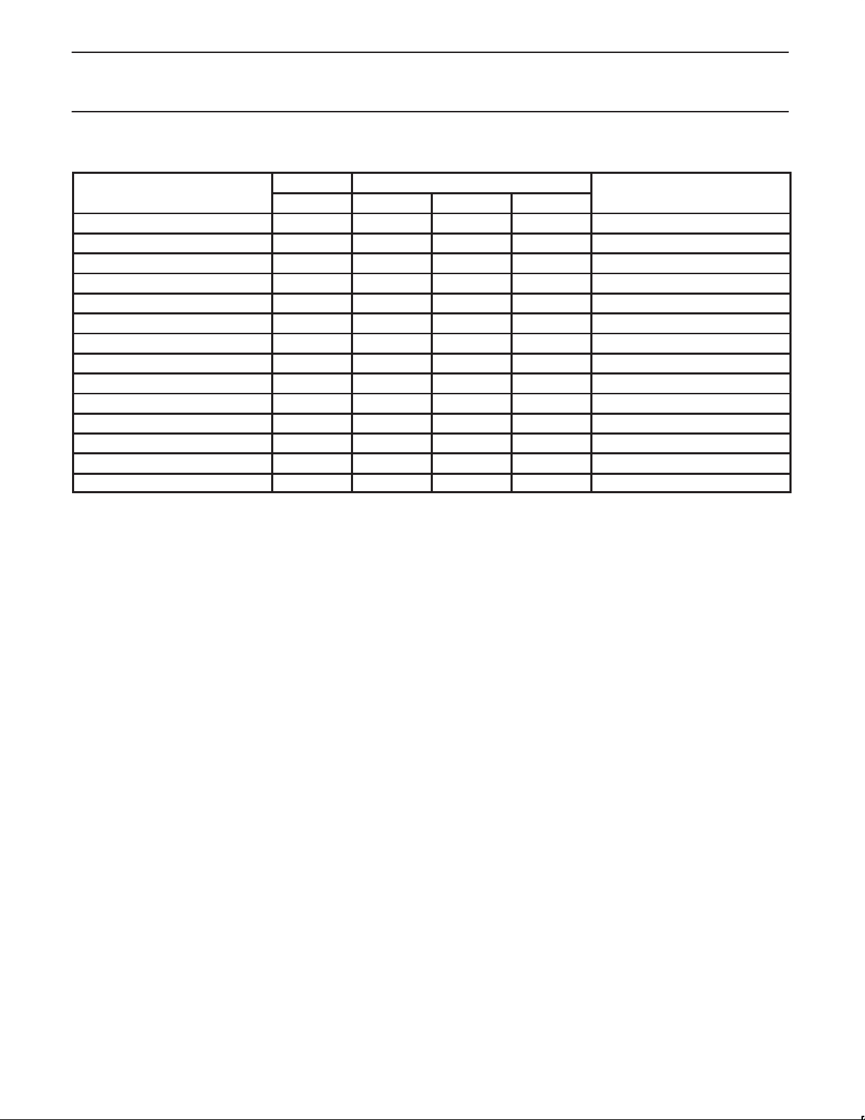
Table 7. Measured Tx Output Noise Floor
dBc/Hz
MIN TYP MAX
< 860 –135
860 to 880 –134
880.2 to 890 –133 EGSM TX extension
890 to 915 –133 GSM TX
915 to 925 –133
925.2 to 935 –134 EGSM RX extension
935 to 960 –135 GSM RX
960 to 1000 –135
1000 to 1710 –135
1710 to 1785 –146 DCS1800 TX
1785 to 1805 –145
1805 to 1880 –144 DCS1800 RX
1880 to 12750 –147
Adjacent Channel –130
1997 May 22
16
Page 17
Philips Semiconductors Product specification
SA1620Low voltage GSM front-end transceiver
5
4.5
4
3V
3.5
Icc (mA)
2.5
4V
3
2
-40° 25° 85°
5V
Temp (°C)
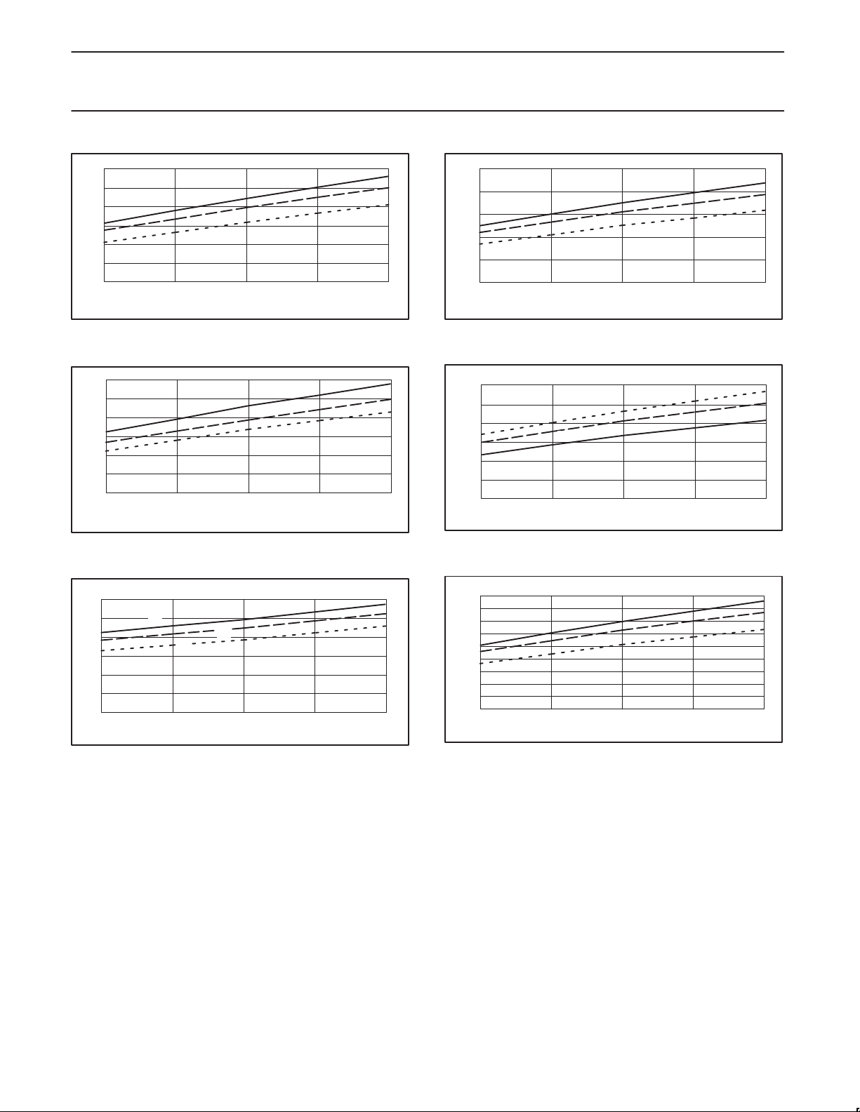
Figure 5. LNA1_ICC vs. Temp
5
4.5
4
3V
3.5
Icc (mA)
2.5
4V
3
2
-40° 25° 85°
5V
Temp (°C)
Figure 6. LNA_2 ICC vs. Temp
SR01334
SR01339
40
35
30
3V
4V
25
Icc (mA)
20
15
5V
-40° 25° 85°
Temp (°C)
Figure 8. Receive ICC vs. Temp
10
9
8
7
Icc (mA)
6
5
4
-40° 25° 85°
5V
4V
3V
Temp (°C)
Figure 9. Standby_ICC vs. Temp
SR01333
SR01338
70
65
60
55
Icc (mA)
50
45
40
-40° 25° 85°
5V
4V
3V
Temp (°C)
Figure 7. Transmit_ICC vs. Temp
SR01344
28
26
24
22
20
18
Icc (mA)
16
14
12
10
-40° 25° 85°
3V
4V
5V
Temp (°C)
Figure 10. Calibrate_ICC vs. Temp
SR01337
1997 May 22
17
Page 18
Philips Semiconductors Product specification
SA1620Low voltage GSM front-end transceiver
34
32
30
28
26
GAIN (dB)
24
22
20
-40° 25° 85°
Temp (°C)
3V
4V
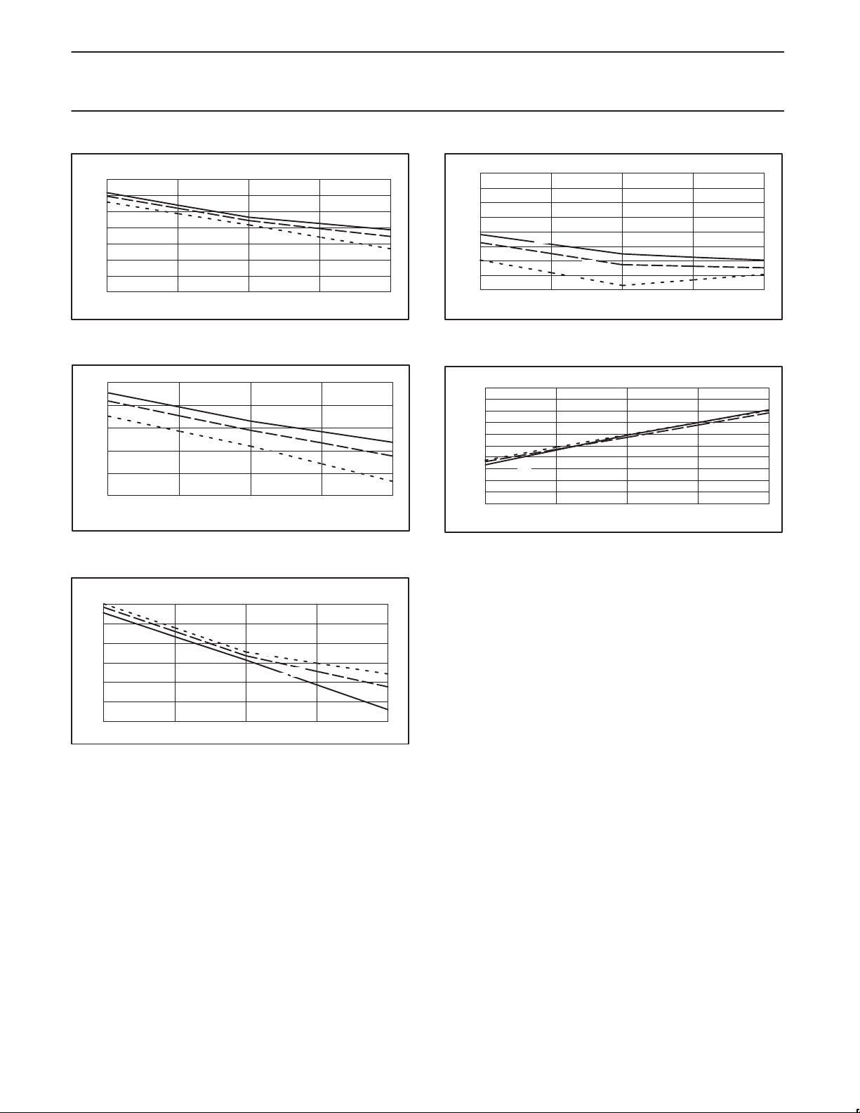
Figure 11. Receive_Gain Mode1 vs. Temp
15
13
11
9
GAIN (dB)
7
5
-40° 25° 85°
3V
4V
5V
Temp (°C)
Figure 12. Receive_Gain_Mode2 vs. Temp
5V
SR01342
SR01335
-20
-22
-24
-26
-28
-30
GAIN (dB)
-32
-34
-36
-40° 25° 85°
3V
4V
5V
Temp (°C)
Figure 14. Receive_Gain_Mode4 vs. Temp
-15
-16
-17
-18
-19
-20
-21
IP3 (dBm)
-22
-23
-24
-25
-40° 25° 85°
5V
4V
3V
Temp (°C)
Figure 15. Receive IIP3 vs. Temp
SR01336
SR01343
0
-1
-2
-3
GAIN (dB)
-4
-5
-6
-40° 25° 85°
Temp (°C)
5V
4V
3V
Figure 13. Receive_Gain_Mode3 vs. Temp
SR01341
1997 May 22
18
Page 19
Philips Semiconductors Product specification
SA1620Low voltage GSM front-end transceiver
2.0
1.9
1.8
NOISE FIGURE (dB)
1.7
1.6
–40 0 25 85
5.0V
2.7V
TEMPERATURE (°C)
3.0V
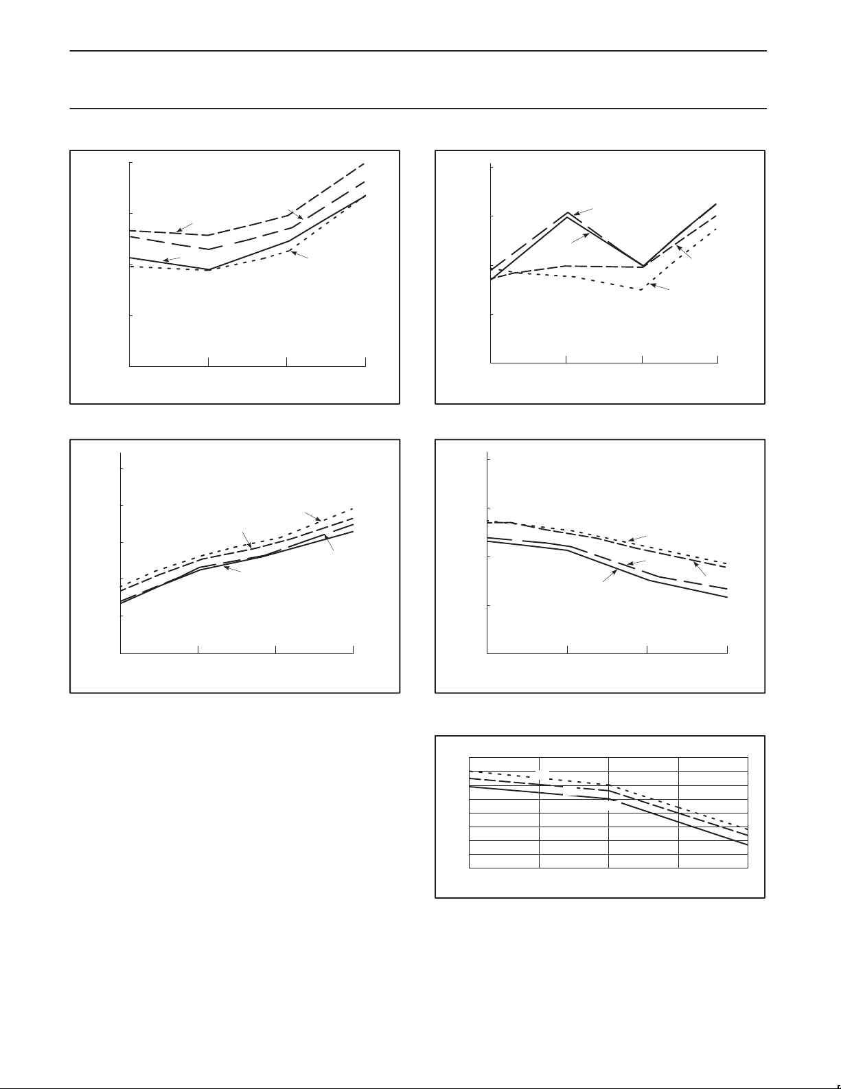
Figure 16. Receive LNA1 Noise Figure
2.50
2.30
5.0V
2.10
1.90
1.70
NOISE FIGURE (dB)
1.50
–40 0 25 85
TEMPERATURE (°C)
2.7V
5.5V
Figure 17. Receive LNA2 Noise Figure
5.5V
3.0V
SR00134
SR00137
10.80
10.40
2.7V
10.00
NOISE FIGURE (dB)
9.60
9.20
–40 0 25 85
3.0V
5.5V
TEMPERATURE (°C)
Figure 18. Receive Mixer Noise Figure
10.00
9.00
5.5V
8.00
POWER (dBm)
7.00
6.00
–40 0 25 85
2.7V
TEMPERATURE (°C)
3.0V
Figure 19. Transmit Power @ -25dBm
5.0V
SR00140
5.0V
SR00149
1997 May 22
19
12
11
10
9
8
7
6
POWER (dBm)
5
4
-40° 25° 85°
5V
4V
3V
Temp (°C)
Figure 20. Transmit_Power @ –20 dBm Input
SR01345
Page 20
Philips Semiconductors Product specification
SA1620Low voltage GSM front-end transceiver
9.50
9.00
5.0V
8.50
POWER (dBm)
8.00
7.50
7.00
–40 0 25 85
TEMPERATURE (°C)
2.7V
5.5V
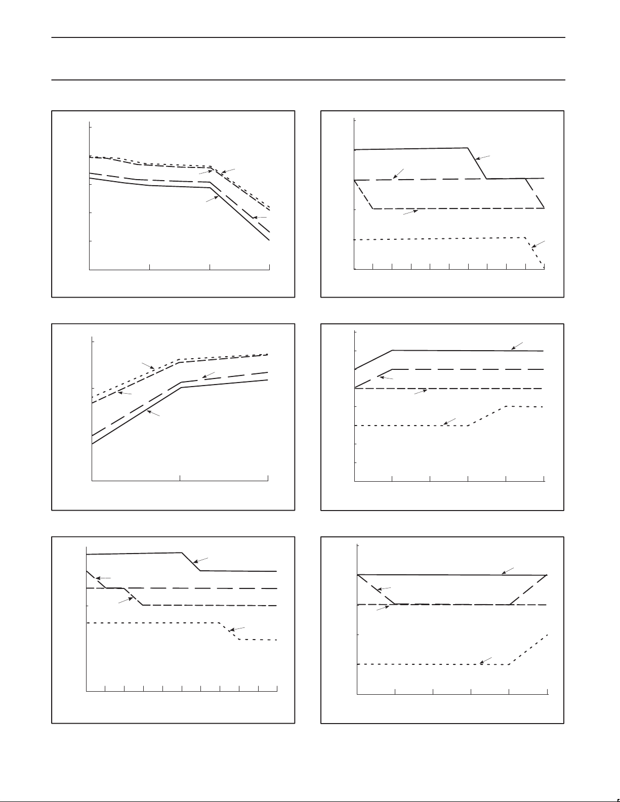
Figure 21. Transmit Power @ -15dBm
9.00
8.50
8.00
POWER (dBm)
5.5V
5.0V
2.7V
3.0V
3.0V
SR00150
3.02
3.01
0
3.00
2.99
Vreg (Volts)
2.98
2.97
036912
25
15 18 21 24 27 30
FORCED CURRENT (mA)
Figure 24. Regulator 2 Load Regulation (V
3.01
3.00
2.99
0
25
85
Vreg (Volts)
2.98
2.97
2.96
–40
BATT
85
SR00153
= 3.5V)
–40
7.50
7.00
–25.00 –20.00 –15.00
INPUT POWER (dBm)
Figure 22. Transmit Power @ 25°C
–40
0
2.98
Vreg (Volts)
2.93
25
010203040
FORCED CURRENT (mA)
50 60 70 80 90 100
Figure 23. Regulator 1 Load Regulation (V
BATT
SR00151
85
SR00152
= 3.5V)
2.95
2.94
2.93
3.3 3.5 4.5
FORCED CURRENT (mA)
5.5 6.5 7.5
SR00154
Figure 25. Regulator 1 Line Regulation @ 100mA Load
3.01
3.00
0
2.99
25
2.98
Vreg (Volts)
2.97
2.96
3.3 3.5 4.5
5.5 6.5 7.5
FORCED CURRENT (mA)
–40
85
SR00155
Figure 26. Regulator 2 Line Regulation @ 30mA Load
1997 May 22
20
Page 21
Philips Semiconductors Product specification
SA1620Low voltage GSM front-end transceiver
12
10
8
6
4
2
0
-2
-4
TRANSMITTER POWER (dBm)
130
150
180
220
240
270
300
330
360
R546 (Ω)
430
VCC = 3V
Temp = 25°C
510
560
620
750
820
910
SR00156
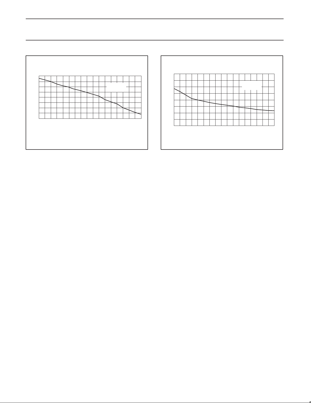
Figure 27. Transmit Output Power vs R(546) @ VCC = 3V
1000
100
90
80
70
60
50
CURRENT (mA)
40
30
20
130
150
180
220
240
270
300
330
360
R546 (Ω)
430
VCC = 3V
Temp = 25°C
510
560
620
750
820
SR00157
910
Figure 28. Transmit Mode Current vs R(546) @ VCC = 3V
1000
1997 May 22
21
Page 22
Philips Semiconductors Product specification
SA1620Low voltage GSM front-end transceiver
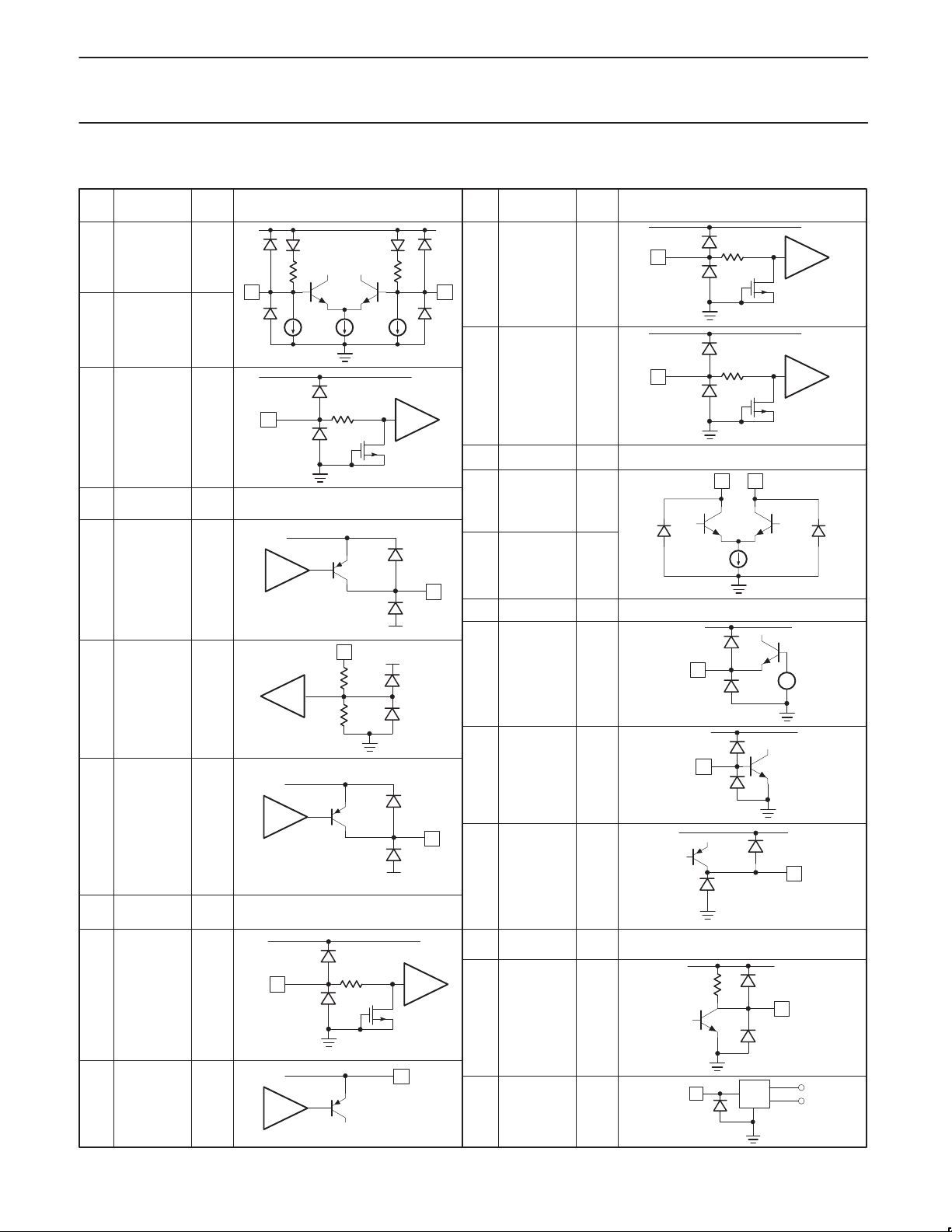
PIN FUNCTIONS
PIN
No.
PIN
MNEMONIC
DC V EQUIVALENT CIRCUIT
PIN
No.
PIN
MNEMONIC
DC V EQUIVALENT CIRCUIT
1VCC3.0
2 IN2 0.8
3 GNDL2 0.0
4 GNDL2a 0.0
5 OUT2 2.2
B
6
CMOS
INPUT
1
12
12 VCCBM 3.0
13 GND 0.0
2
14
POnRx
CMOS
14
—
+
INPUT
15 GND 0.0
5
16 Rxif 3.0
16 17
17 RxifX 3.0
6
—
+
18 GND 0.0
19 Txif 2.2
A
7
CMOS
INPUT
8 INM 0.4
9 INMX 0.4
10 COMP2 2.2
11 COMP1 2.2
19 20
7
—
+
20 TxifX 2.2
21 GND 0.0
22
8
22 V
Tx 3.0
CC
23 GND 0.0
24
24 VCCTx 3.0
9
25 GND 0.0
or
11
10
26
CON2
CMOS
26
—
+
INPUT
SR00162
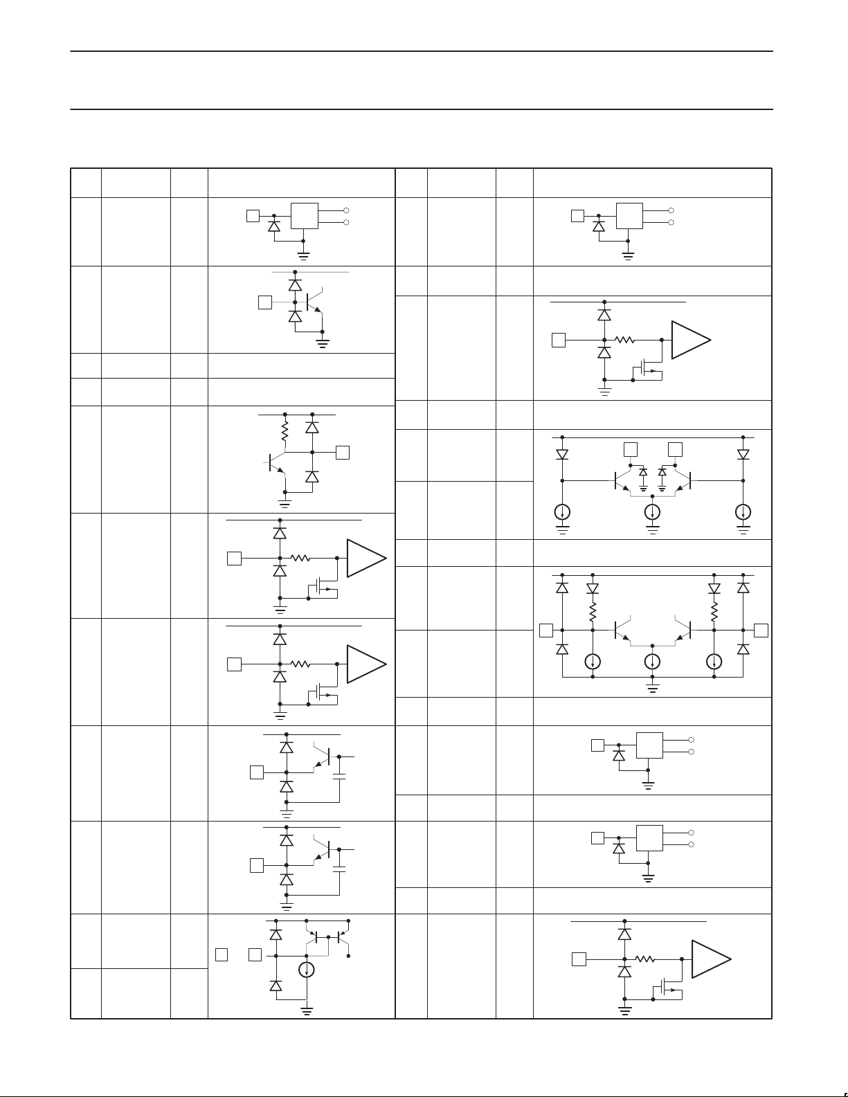
Figure 29. Pin Functions
1997 May 22
22
Page 23
Philips Semiconductors Product specification
SA1620Low voltage GSM front-end transceiver
PIN FUNCTIONS (continued)
PIN
No.
PIN
MNEMONIC
DC V EQUIVALENT CIRCUIT
PIN
No.
PIN
MNEMONIC
DC V EQUIVALENT CIRCUIT
27 LOin 2.2
28 LOinX 2.2
CON1
29
CMOS
INPUT
30 GndReg1 0.0
31 VReg2 3.0
32 VRegF2 3.0
27 28
V
—
V
BATT
+
BATT
31
GndReg2
29
—
+
32
—
+
POnBuf
37
CMOS
INPUT
PDTx
38
CMOS
INPUT
39 GndTx 0.0
40 TxOx 3.0
41 TxO 3.0
42 GndTx 0.0
43 RETx 0.4
37
38
40 41
43
—
+
—
+
+
–
33 VReg1 3.0
34 GndReg1 0.0
POn
CMOS
35
INPUT
36 V
BATT
3.0
GndReg2
V
BATT
—
+
33
GndReg1
44 IN1 0.8
45 GndL1 0.0
44
45
46 GndTx 0.0
35
—
+
—
+
47 OUT1 2.2
36
48
47
48 VCCL1 3.0
SR00163
Figure 29. Pin Functions (continued)
1997 May 22
23
Page 24
Philips Semiconductors Product specification
SA1620Low voltage GSM front-end transceiver
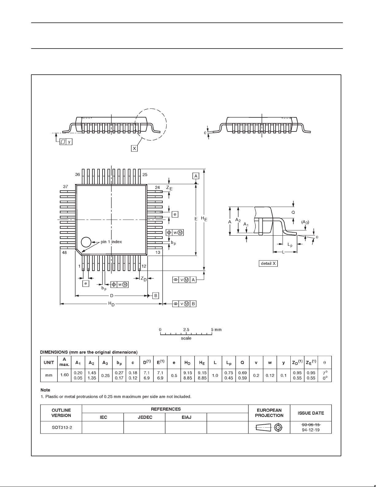
LQFP48: plastic low profile quad flat package; 48 leads; body 7 x 7 x 1.4 mm SOT313-2
1997 May 22
24
Page 25

Philips Semiconductors Product specification
SA1620Low voltage GSM front-end transceiver
NOTES
1997 May 22
25
Page 26

Philips Semiconductors Product specification
SA1620Low voltage GSM front-end transceiver
DEFINITIONS
Data Sheet Identification Product Status Definition
Objective Specification
Preliminary Specification
Product Specification
Formative or in Design
Preproduction Product
Full Production
Philips Semiconductors and Philips Electronics North America Corporation reserve the right to make changes, without notice, in the products,
including circuits, standard cells, and/or software, described or contained herein in order to improve design and/or performance. Philips
Semiconductors assumes no responsibility or liability for the use of any of these products, conveys no license or title under any patent, copyright,
or mask work right to these products, and makes no representations or warranties that these products are free from patent, copyright, or mask
work right infringement, unless otherwise specified. Applications that are described herein for any of these products are for illustrative purposes
only. Philips Semiconductors makes no representation or warranty that such applications will be suitable for the specified use without further testing
or modification.
LIFE SUPPORT APPLICA TIONS
Philips Semiconductors and Philips Electronics North America Corporation Products are not designed for use in life support appliances, devices,
or systems where malfunction of a Philips Semiconductors and Philips Electronics North America Corporation Product can reasonably be expected
to result in a personal injury. Philips Semiconductors and Philips Electronics North America Corporation customers using or selling Philips
Semiconductors and Philips Electronics North America Corporation Products for use in such applications do so at their own risk and agree to fully
indemnify Philips Semiconductors and Philips Electronics North America Corporation for any damages resulting from such improper use or sale.
Philips Semiconductors
811 East Arques Avenue
P.O. Box 3409
Sunnyvale, California 94088–3409
Telephone 800-234-7381
This data sheet contains the design target or goal specifications for product development. Specifications
may change in any manner without notice.
This data sheet contains preliminary data, and supplementary data will be published at a later date. Philips
Semiconductors reserves the right to make changes at any time without notice in order to improve design
and supply the best possible product.
This data sheet contains Final Specifications. Philips Semiconductors reserves the right to make changes
at any time without notice, in order to improve design and supply the best possible product.
Copyright Philips Electronics North America Corporation 1997
All rights reserved. Printed in U.S.A.
1997 May 22
26
 Loading...