

Page 1
S822T/S822TW/S822TRW
Silicon NPN Planar RF Transistor
Observe precautions for handling.
Electrostatic sensitive device.
Applications
For low noise and high gain broadband amplifiers at
collector currents from 0.2 mA to 5 mA.
Features
D
Low supply voltage
D
Low current consumption
D
50 W input impedance at 945 MHz
D
Low noise figure
D
High power gain
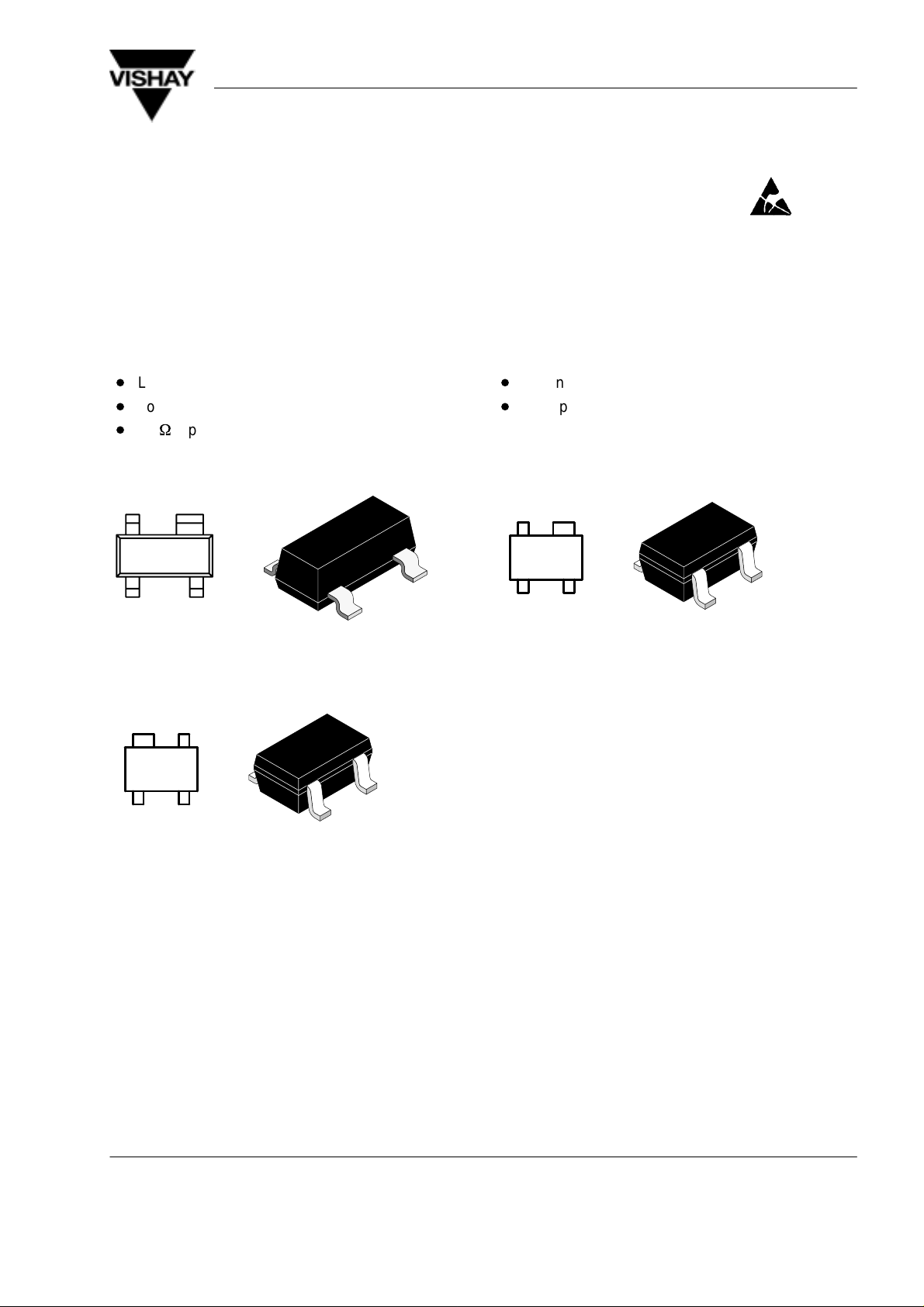
Vishay Telefunken
21
94 9279
13 579
43
S822T Marking: 822
Plastic case (SOT 143)
1 = Collector, 2 = Emitter, 3 = Base, 4 = Emitter
2
1
13 56613 654
34
S822TRW Marking: WSF
Plastic case (SOT 343R)
1 = Collector, 2 = Emitter, 3 = Base, 4 = Emitter
1
2
13 653
3
4
S822TW Marking: W22
Plastic case (SOT 343)
1 = Collector, 2 = Emitter, 3 = Base, 4 = Emitter
13 566
Document Number 85050
Rev. 3, 20-Jan-99
www.vishay.de • FaxBack +1-408-970-5600
1 (8)
Page 2
S822T/S822TW/S822TRW
Transition frequency
f
g
e ot
Real part of input impedance
Re
Vishay Telefunken
Absolute Maximum Ratings
T
= 25_C, unless otherwise specified
amb
Parameter Test Conditions Symbol Value Unit
Collector-base voltage V
Collector-emitter voltage V
Emitter-base voltage V
Collector current I
Total power dissipation T
≤ 125 °C P
amb
Junction temperature T
Storage temperature range T
CBO
CEO
EBO
C
tot
j
stg
Maximum Thermal Resistance
T
= 25_C, unless otherwise specified
amb
Parameter T est Conditions Symbol Value Unit
Junction ambient on glass fibre printed board (25 x 20 x 1.5) mm
3
R
thJA
plated with 35mm Cu
Electrical DC Characteristics
T
= 25_C, unless otherwise specified
amb
Parameter Test Conditions Symbol Min Typ Max Unit
Collector cut-off current VCE = 12 V, VBE = 0 I
Collector-base cut-off current VCB = 8 V, IE = 0 I
Emitter-base cut-off current VEB = 1 V, IC = 0 I
Collector-emitter breakdown voltage IC = 1 mA, IB = 0 V
Collector-emitter saturation voltage IC = 5 mA, IB = 0.5 mA V
DC forward current transfer ratio VCE = 3 V, IC = 1 mA h
CES
CBO
EBO
(BR)CEO
CEsat
FE
12 V
6 V
2 V
8 mA
30 mW
150
–65 to +150
450 K/W
6 V
0.1 0.4 V
40 90 150
°
C
°
C
100mA
100 nA
1
m
A
Electrical AC Characteristics
T
= 25_C, unless otherwise specified
amb
Parameter Test Conditions Symbol Min Typ Max Unit
VCE = 3 V, IC = 1 mA, f = 500 MHz
VCE = 2 V, IC = 1.5 mA, f = 500 MHz
Collector-base capacitance VCB = 1 V, f = 1 MHz C
ZS = Z
2 V, I
Noise figure
ZS = Z
3 V, IC = 1 mA
ZS = Z
2 V, IC = 1.5 mA
VCE = 2 V, IC = 0.5 mA, f = 450MHz 13.5 dB
Power gain VCE = 3 V, IC = 1 mA, f = 945 MHz Gpe @F
VCE = 2 V, IC = 1.5 mA, f = 945 MHz
Collector current for fT max VCE = 2 V, f = 500 MHz I
p
www.vishay.de • FaxBack +1-408-970-5600
2 (8)
p
p
VCE = 3 V, IC = 1 mA, f = 945 MHz
VCE = 2 V, IC = 1.5 mA, f = 945 MHz
, f = 450 MHz, VCE =
Sopt
= 0.5 mA
C
, f = 945 MHz, VCE =
Sopt
, f = 945 MHz, VCE =
Sopt
F
opt
(h11e)
T
cb
C
opt
4.7 GHz
5.2 GHz
0.2 pF
1.1 dB
1.8 dB
2 dB
12.5 dB
14.0 dB
3 mA
50
50
Document Number 85050
Rev. 3, 20-Jan-99
W
W
Page 3
Common Emitter S–Parameters
VCE/V
IC/mA
f/MHz
2
S822T/S822TW/S822TRW
Vishay Telefunken
Z0 = 50 W,
T
= 25_C, unless otherwise specified
amb
S11 S21 S12 S22
LIN
MAG
100 0.974 –4.0 1.86 175.2 0.012 86.4 0.997 –2.3
200 0.967 –7.9 1.84 169.7 0.024 82.4 0.993 –4.8
300 0.956 –11.8 1.82 164.2 0.035 78.6 0.87 –6.9
400 0.941 –15.6 1.79 158.9 0.046 75.1 0.979 –9.3
500 0.926 –19.0 1.75 153.9 0.056 71.7 0.968 –11.4
600 0.907 –22.5 1.72 149.2 0.066 69.0 0.959 –13.1
0.5 700 0.890 –25.8 1.68 145.0 0.075 66.4 0.951 –15.2
800 0.870 –29.3 1.66 141.0 0.084 63.9 0.940 –16.9
900 0.851 –32.3 1.63 136.1 0.092 61.1 0.930 –18.8
1000 0.833 –35.6 1.60 132.6 0.099 59.0 0.924 –20.4
1100 0.814 –39.0 1.58 128.6 0.108 56.9 0.913 –22.2
1200 0.794 –42.4 1.57 124.9 0.115 54.8 0.904 –24.0
1300 0.773 –45.6 1.55 121.2 0.121 52.7 0.895 –25.7
100 0.919 –6.9 4.86 171.8 0.012 84.3 0.992 –3.6
200 0.897 –13.7 4.78 163.4 0.023 78.4 0.979 –7.1
300 0.864 –19.8 4.62 155.7 0.034 73.0 0.957 –10.2
400 0.824 –25.7 4.41 148.3 0.043 68.4 0.933 –13.0
500 0.781 –31.0 4.21 141.3 0.051 64.0 0.909 –15.6
600 0.735 –36.1 4.00 135.3 0.058 60.6 0.881 –17.3
1.5 700 0.693 –40.5 3.82 129.4 0.064 58.2 0.858 –19.2
800 0.647 –44.6 3.62 124.3 0.071 54.7 0.836 –20.7
900 0.605 –48.5 3.46 118.9 0.076 52.0 0.814 –22.3
1000 0.567 –52.4 3.30 114.3 0.081 49.8 0.796 –23.6
1100 0.526 –56.4 3.16 110.0 0.085 48.1 0.778 –24.9
1200 0.491 –60.1 3.04 105.7 0.090 46.1 0.763 –26.3
1300 0.458 –64.4 2.92 102.0 0.094 44.9 0.747 –27.5
ANG
deg deg deg deg
LIN
MAG
ANG
LIN
MAG
ANG
LIN
MAG
ANG
Document Number 85050
Rev. 3, 20-Jan-99
www.vishay.de • FaxBack +1-408-970-5600
3 (8)
Page 4

S822T/S822TW/S822TRW
Vishay Telefunken
Typical Characteristics (T
50
40
30
20
10
tot
P – Total Power Dissipation ( mW )
0
0 25 50 75 100 125 150
T
– Ambient Temperature ( °C )13619
amb
Figure 1.. Total Power Dissipation vs.
Ambient Temperature
7000
6000
5000
f=500MHz
= 25_C unless otherwise specified)
amb
0.5
0.4
0.3
0.2
0.1
cb
C – Collector Base Capacitance ( pF )
0
012345
VCB – Collector Base Voltage ( V )13621
Figure 3.. Collector Base Capacitance vs.
Collector Base Voltage
3V
2V
4000
3000
2000
1000
T
f – Transition Frequency ( MHz )
0
012345
IC – Collector Current ( mA )13620
VCE=1V
Figure 2.. Transition Frequency vs. Collector Current
www.vishay.de • FaxBack +1-408-970-5600
4 (8)
Document Number 85050
Rev. 3, 20-Jan-99
Page 5

S822T/S822TW/S822TRW
Vishay Telefunken
VCE = 2 V, IC = 1.5 mA , Z0 = 50
S
11
j
S
21
j0.5
j0.2
0
–j0.2
13 558
0.2
–j0.5
0.5
1
1300MHz
–j
Figure 4.. Input reflection coefficient
2
900
–j2
j2
5
500
–j5
j5
100
W
S
12
90°
120°
150°
1
180°
–150°
–120° –60°
13 559
500
100
–90°
60°
1300MHz
900
0.04 0.08
30°
0°
–30°
Figure 6.. Reverse transmission coefficient
S
22
90°
120°
900
500
150°
100
180°
–150°
–120° –60°
13 560
1300MHz
2 4
–90°
Figure 5.. Forward transmission coefficient
60°
30°
–30°
j
j0.5
j0.2
0°
0
–j0.2
13 561
0.2
–j0.5
0.5
1
–j
2
1300MHz
–j2
j2
5
500
100
j5
1
–j5
Figure 7.. Output reflection coefficient
Document Number 85050
Rev. 3, 20-Jan-99
www.vishay.de • FaxBack +1-408-970-5600
5 (8)
Page 6

S822T/S822TW/S822TRW
Vishay Telefunken
Dimensions of S822T in mm
Dimensions of S822TW in mm
96 12240
www.vishay.de • FaxBack +1-408-970-5600
6 (8)
96 12237
Document Number 85050
Rev. 3, 20-Jan-99
Page 7

Dimensions of S822TRW in mm
S822T/S822TW/S822TRW
Vishay Telefunken
96 12238
Document Number 85050
Rev. 3, 20-Jan-99
www.vishay.de • FaxBack +1-408-970-5600
7 (8)
Page 8

S822T/S822TW/S822TRW
Vishay Telefunken
Ozone Depleting Substances Policy Statement
It is the policy of Vishay Semiconductor GmbH to
1. Meet all present and future national and international statutory requirements.
2. Regularly and continuously improve the performance of our products, processes, distribution and operating
systems with respect to their impact on the health and safety of our employees and the public, as well as their
impact on the environment.
It is particular concern to control or eliminate releases of those substances into the atmosphere which are known as
ozone depleting substances (ODSs).
The Montreal Protocol (1987) and its London Amendments (1990) intend to severely restrict the use of ODSs and
forbid their use within the next ten years. V arious national and international initiatives are pressing for an earlier ban
on these substances.
Vishay Semiconductor GmbH has been able to use its policy of continuous improvements to eliminate the use of
ODSs listed in the following documents.
1. Annex A, B and list of transitional substances of the Montreal Protocol and the London Amendments respectively
2. Class I and II ozone depleting substances in the Clean Air Act Amendments of 1990 by the Environmental
Protection Agency (EPA) in the USA
3. Council Decision 88/540/EEC and 91/690/EEC Annex A, B and C (transitional substances) respectively.
Vishay Semiconductor GmbH can certify that our semiconductors are not manufactured with ozone depleting
substances and do not contain such substances.
We reserve the right to make changes to improve technical design and may do so without further notice.
Parameters can vary in different applications. All operating parameters must be validated for each customer application
by the customer. Should the buyer use Vishay-Telefunken products for any unintended or unauthorized application, the
buyer shall indemnify Vishay-Telefunken against all claims, costs, damages, and expenses, arising out of, directly or
indirectly , any claim of personal damage, injury or death associated with such unintended or unauthorized use.
Vishay Semiconductor GmbH, P.O.B. 3535, D-74025 Heilbronn, Germany
Telephone: 49 (0)7131 67 2831, Fax number: 49 (0)7131 67 2423
www.vishay.de • FaxBack +1-408-970-5600
8 (8)
Document Number 85050
Rev. 3, 20-Jan-99
 Loading...