

Page 1

S25FL032A
32 Megabit CMOS 3.0 Volt Flash Memory
with 50-MHz SPI (Serial Peripheral Interface) Bus
Data Sheet
Notice to Readers: This document states the current technical specifications regarding the Spansion
product(s) described herein. Each product described herein may be designated as Advance Information,
Preliminary, or Full Production. See Notice On Data Sheet Designations for definitions.
S25FL032A Cover Sheet
Publication Number S25FL032A_00 Revision C Amendment 2 Issue Date July 2, 2007
Page 2

Notice On Data Sheet Designations
Spansion Inc. issues data sheets with Advance Information or Preliminary designations to advise readers of
product information or intended specifications throughout the product life cycle, including development,
qualification, initial production, and full production. In all cases, however, readers are encouraged to verify
that they have the latest information before finalizing their design. The following descriptions of Spansion data
sheet designations are presented here to highlight their presence and definitions.
Advance Information
The Advance Information designation indicates that Spansion Inc. is developing one or more specific
products, but has not committed any design to production. Information presented in a document with this
designation is likely to change, and in some cases, development on the product may discontinue. Spansion
Inc. therefore places the following conditions upon Advance Information content:
“This document contains information on one or more products under development at Spansion Inc.
The information is intended to help you evaluate this product. Do not design in this product without
contacting the factory. Spansion Inc. reserves the right to change or discontinue work on this proposed
product without notice.”
Preliminary
The Preliminary designation indicates that the product development has progressed such that a commitment
to production has taken place. This designation covers several aspects of the product life cycle, including
product qualification, initial production, and the subsequent phases in the manufacturing process that occur
before full production is achieved. Changes to the technical specifications presented in a Preliminary
document should be expected while keeping these aspects of production under consideration. Spansion
places the following conditions upon Preliminary content:
“This document states the current technical specifications regarding the Spansion product(s)
described herein. The Preliminary status of this document indicates that product qualification has been
completed, and that initial production has begun. Due to the phases of the manufacturing process that
require maintaining efficiency and quality, this document may be revised by subsequent versions or
modifications due to changes in technical specifications.”
Data Sheet
Combination
Some data sheets contain a combination of products with different designations (Advance Information,
Preliminary, or Full Production). This type of document distinguishes these products and their designations
wherever necessary, typically on the first page, the ordering information page, and pages with the DC
Characteristics table and the AC Erase and Program table (in the table notes). The disclaimer on the first
page refers the reader to the notice on this page.
Full Production (No Designation on Document)
When a product has been in production for a period of time such that no changes or only nominal changes
are expected, the Preliminary designation is removed from the data sheet. Nominal changes may include
those affecting the number of ordering part numbers available, such as the addition or deletion of a speed
option, temperature range, package type, or V
description or to correct a typographical error or incorrect specification. Spansion Inc. applies the following
conditions to documents in this category:
“This document states the current technical specifications regarding the Spansion product(s)
described herein. Spansion Inc. deems the products to have been in sufficient production volume such
that subsequent versions of this document are not expected to change. However, typographical or
specification corrections, or modifications to the valid combinations offered may occur.”
Questions regarding these document designations may be directed to your local sales office.
range. Changes may also include those needed to clarify a
IO
2 S25FL032A S25FL032A_00_C2 July 2, 2007
Page 3

S25FL032A
32 Megabit CMOS 3.0 Volt Flash Memory
with 50-MHz SPI (Serial Peripheral Interface) Bus
Data Sheet
Distinctive Characteristics
Architectural Advantages
Single power supply operation
– Full voltage range: 2.7 to 3.6 V read and program operations
Memory Architecture
– 64 sectors with 512 Kb each
Program
– Page Program (up to 256 bytes) in 1.4 ms (typical)
– Program operations are on a page by page basis
Erase
– 0.5 s typical sector erase time
– Bulk erase function
Cycling Endurance
– 100,000 cycles per sector typical
Data Retention
– 20 years typical
Device ID
– JEDEC standard two-byte electronic signature
– RES command one-byte electronic signature for backward
compatibility
General Description
The S25FL032A is a 3.0 Volt (2.7 V to 3.6 V), single-power-supply Flash memory device. The device consists
of 64 sectors, each with 512 Kb memory.
The device accepts data written to SI (Serial Input) and outputs data on SO (Serial Output). The devices are
designed to be programmed in-system with the standard system 3.0 volt VCC supply.
The memory can be programmed 1 to 256 bytes at a time, using the Page Program command. The device
supports Sector Erase and Bulk Erase commands.
Each device requires only a 3.0 volt power supply (2.7 V to 3.6 V) for both read and write functions. Internally
generated and regulated voltages are provided for the program operations. This device does not require a
supply.
V
PP
Process Technology
– Manufactured on 0.20 µm MirrorBit® process technology
Package Option
– Industry Standard Pinouts
– 16-pin SO package (300 mils)
Performance Characteristics
Speed
– 50 MHz clock rate (maximum)
Power Saving Standby Mode
– Standby Mode 50 µA (max)
– Deep Power Down Mode 2 µA (typical)
Memory Protection Features
Memory Protection
– W# pin works in conjunction with Status Register Bits to protect
specified memory areas
– Status Register Block Protection bits (BP2, BP1, BP0) in status
register configure parts of memory as read-only
Software Features
– SPI Bus Compatible Serial Interface
Publication Number S25FL032A_00 Revision C Amendment 2 Issue Date July 2, 2007
Page 4

Table of Contents
Distinctive Characteristics. . . . . . . . . . . . . . . . . . . . . . . . . . . . . . . . . . . . . . . . . . . . . . . . . . . . . . . . . . . . . . 3
General Description . . . . . . . . . . . . . . . . . . . . . . . . . . . . . . . . . . . . . . . . . . . . . . . . . . . . . . . . . . . . . . . . . . . 3
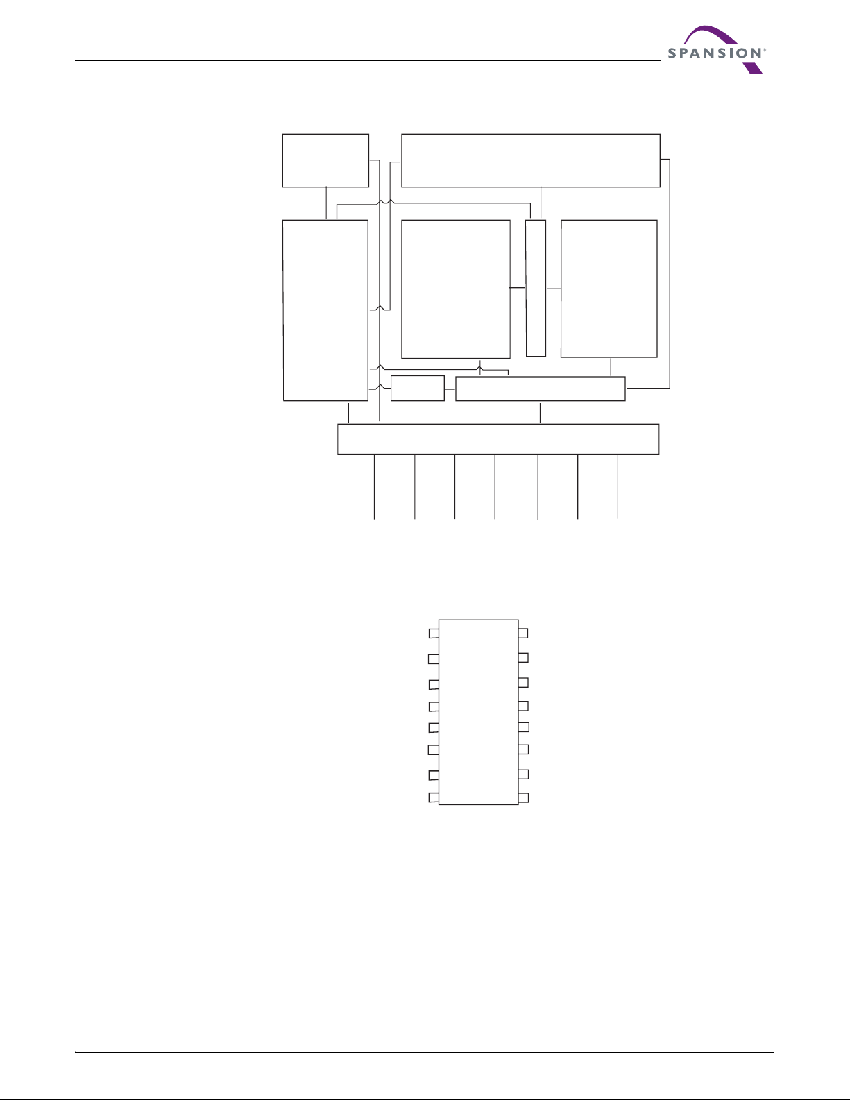
1. Block Diagram . . . . . . . . . . . . . . . . . . . . . . . . . . . . . . . . . . . . . . . . . . . . . . . . . . . . . . . . . . . . . . . . . . . 7
2. Connection Diagrams . . . . . . . . . . . . . . . . . . . . . . . . . . . . . . . . . . . . . . . . . . . . . . . . . . . . . . . . . . . . . 7
3. Input/Output Descriptions. . . . . . . . . . . . . . . . . . . . . . . . . . . . . . . . . . . . . . . . . . . . . . . . . . . . . . . . . . 8
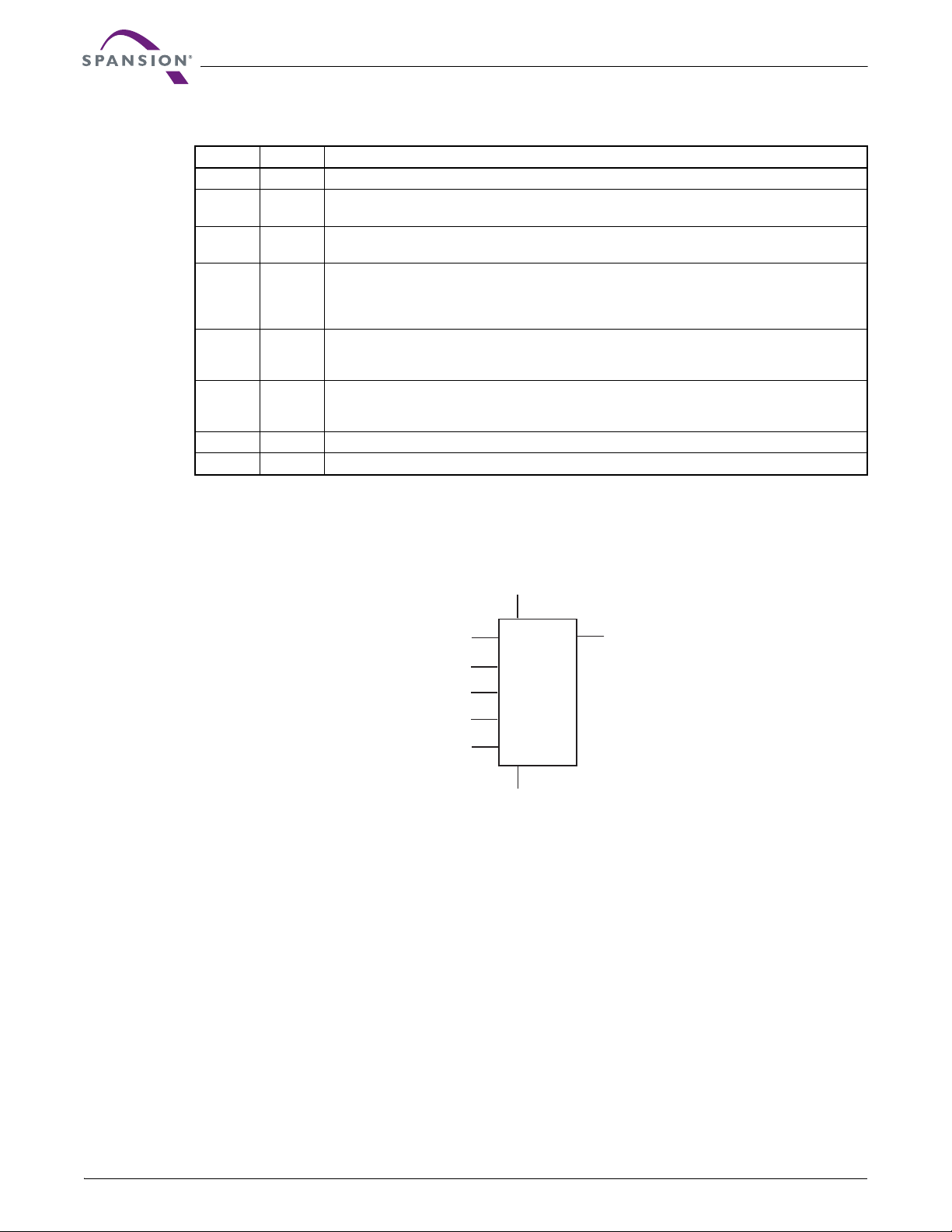
4. Logic Symbol . . . . . . . . . . . . . . . . . . . . . . . . . . . . . . . . . . . . . . . . . . . . . . . . . . . . . . . . . . . . . . . . . . . . 8
5. Ordering Information . . . . . . . . . . . . . . . . . . . . . . . . . . . . . . . . . . . . . . . . . . . . . . . . . . . . . . . . . . . . . . 9
5.1 Valid Combinations . . . . . . . . . . . . . . . . . . . . . . . . . . . . . . . . . . . . . . . . . . . . . . . . . . . . . . . . . 9
6. Spansion SPI Modes . . . . . . . . . . . . . . . . . . . . . . . . . . . . . . . . . . . . . . . . . . . . . . . . . . . . . . . . . . . . . 10
7. Device Operations . . . . . . . . . . . . . . . . . . . . . . . . . . . . . . . . . . . . . . . . . . . . . . . . . . . . . . . . . . . . . . . 11
7.1 Byte or Page Programming . . . . . . . . . . . . . . . . . . . . . . . . . . . . . . . . . . . . . . . . . . . . . . . . . . 11
7.2 Sector Erase / Bulk Erase . . . . . . . . . . . . . . . . . . . . . . . . . . . . . . . . . . . . . . . . . . . . . . . . . . . 11
7.3 Monitoring Write Operations Using the Status Register . . . . . . . . . . . . . . . . . . . . . . . . . . . . 11
7.4 Active Power and Standby Power Modes . . . . . . . . . . . . . . . . . . . . . . . . . . . . . . . . . . . . . . . 11
7.5 Status Register . . . . . . . . . . . . . . . . . . . . . . . . . . . . . . . . . . . . . . . . . . . . . . . . . . . . . . . . . . . 11
7.6 Data Protection Modes . . . . . . . . . . . . . . . . . . . . . . . . . . . . . . . . . . . . . . . . . . . . . . . . . . . . . 12
7.7 Hold Mode (HOLD#) . . . . . . . . . . . . . . . . . . . . . . . . . . . . . . . . . . . . . . . . . . . . . . . . . . . . . . . 13
8. Sector Address Table . . . . . . . . . . . . . . . . . . . . . . . . . . . . . . . . . . . . . . . . . . . . . . . . . . . . . . . . . . . . . 13
9. Command Definitions . . . . . . . . . . . . . . . . . . . . . . . . . . . . . . . . . . . . . . . . . . . . . . . . . . . . . . . . . . . . 15
9.1 Read Data Bytes (READ) . . . . . . . . . . . . . . . . . . . . . . . . . . . . . . . . . . . . . . . . . . . . . . . . . . . 16
9.2 Read Data Bytes at Higher Speed (FAST_READ) . . . . . . . . . . . . . . . . . . . . . . . . . . . . . . . . 17
9.3 Read Identification (RDID) . . . . . . . . . . . . . . . . . . . . . . . . . . . . . . . . . . . . . . . . . . . . . . . . . . . 18
9.4 Write Enable (WREN) . . . . . . . . . . . . . . . . . . . . . . . . . . . . . . . . . . . . . . . . . . . . . . . . . . . . . . 19
9.5 Write Disable (WRDI). . . . . . . . . . . . . . . . . . . . . . . . . . . . . . . . . . . . . . . . . . . . . . . . . . . . . . . 19
9.6 Read Status Register (RDSR) . . . . . . . . . . . . . . . . . . . . . . . . . . . . . . . . . . . . . . . . . . . . . . . . 20
9.7 Write Status Register (WRSR). . . . . . . . . . . . . . . . . . . . . . . . . . . . . . . . . . . . . . . . . . . . . . . . 21
9.8 Page Program (PP) . . . . . . . . . . . . . . . . . . . . . . . . . . . . . . . . . . . . . . . . . . . . . . . . . . . . . . . . 22
9.9 Sector Erase (SE) . . . . . . . . . . . . . . . . . . . . . . . . . . . . . . . . . . . . . . . . . . . . . . . . . . . . . . . . . 23
9.10 Bulk Erase (BE) . . . . . . . . . . . . . . . . . . . . . . . . . . . . . . . . . . . . . . . . . . . . . . . . . . . . . . . . . . . 23
9.11 Deep Power Down (DP). . . . . . . . . . . . . . . . . . . . . . . . . . . . . . . . . . . . . . . . . . . . . . . . . . . . . 24
9.12 Release from Deep Power Down (RES) . . . . . . . . . . . . . . . . . . . . . . . . . . . . . . . . . . . . . . . . 25
10. Power-up and Power-down . . . . . . . . . . . . . . . . . . . . . . . . . . . . . . . . . . . . . . . . . . . . . . . . . . . . . . . . 26
11. Initial Delivery State . . . . . . . . . . . . . . . . . . . . . . . . . . . . . . . . . . . . . . . . . . . . . . . . . . . . . . . . . . . . . . 27
12. Absolute Maximum Ratings . . . . . . . . . . . . . . . . . . . . . . . . . . . . . . . . . . . . . . . . . . . . . . . . . . . . . . . 28
13. Operating Ranges . . . . . . . . . . . . . . . . . . . . . . . . . . . . . . . . . . . . . . . . . . . . . . . . . . . . . . . . . . . . . . . 28
14. DC Characteristics . . . . . . . . . . . . . . . . . . . . . . . . . . . . . . . . . . . . . . . . . . . . . . . . . . . . . . . . . . . . . . . 29
15. Test Conditions . . . . . . . . . . . . . . . . . . . . . . . . . . . . . . . . . . . . . . . . . . . . . . . . . . . . . . . . . . . . . . . . . 29
16. AC Characteristics . . . . . . . . . . . . . . . . . . . . . . . . . . . . . . . . . . . . . . . . . . . . . . . . . . . . . . . . . . . . . . . 30
17. Physical Dimensions . . . . . . . . . . . . . . . . . . . . . . . . . . . . . . . . . . . . . . . . . . . . . . . . . . . . . . . . . . . . . 33
17.1 SO3 016—16-pin Wide Plastic Small Outline Package (300-mil Body Width) . . . . . . . . . . . 33
18. Revision History . . . . . . . . . . . . . . . . . . . . . . . . . . . . . . . . . . . . . . . . . . . . . . . . . . . . . . . . . . . . . . . . . 34
Data Sheet
4 S25FL032A S25FL032A_00_C2 July 2, 2007
Page 5

Figures
Data Sheet
Figure 2.1 16-pin Plastic Small Outline Package (SO) . . . . . . . . . . . . . . . . . . . . . . . . . . . . . . . . . . . . . . . 7
Figure 6.1 Bus Master and Memory Devices on the SPI Bus. . . . . . . . . . . . . . . . . . . . . . . . . . . . . . . . . 10
Figure 6.2 SPI Modes Supported . . . . . . . . . . . . . . . . . . . . . . . . . . . . . . . . . . . . . . . . . . . . . . . . . . . . . . 10
Figure 7.1 Hold Mode Operation. . . . . . . . . . . . . . . . . . . . . . . . . . . . . . . . . . . . . . . . . . . . . . . . . . . . . . . 13
Figure 9.1 Read Data Bytes (READ) Command Sequence . . . . . . . . . . . . . . . . . . . . . . . . . . . . . . . . . . 16
Figure 9.2 Read Data Bytes at Higher Speed (FAST_READ) Command Sequence . . . . . . . . . . . . . . . 17
Figure 9.3 Read Identification (RDID) Command Sequence and Data-Out Sequence . . . . . . . . . . . . . 18
Figure 9.4 Write Enable (WREN) Command Sequence . . . . . . . . . . . . . . . . . . . . . . . . . . . . . . . . . . . . . 19
Figure 9.5 Write Disable (WRDI) Command Sequence . . . . . . . . . . . . . . . . . . . . . . . . . . . . . . . . . . . . . 19
Figure 9.6 Read Status Register (RDSR) Command Sequence . . . . . . . . . . . . . . . . . . . . . . . . . . . . . . 20
Figure 9.7 Write Status Register (WRSR) Command Sequence . . . . . . . . . . . . . . . . . . . . . . . . . . . . . . 21
Figure 9.8 Page Program (PP) Command Sequence. . . . . . . . . . . . . . . . . . . . . . . . . . . . . . . . . . . . . . . 22
Figure 9.9 Sector Erase (SE) Command Sequence . . . . . . . . . . . . . . . . . . . . . . . . . . . . . . . . . . . . . . . . 23
Figure 9.10 Bulk Erase (BE) Command Sequence. . . . . . . . . . . . . . . . . . . . . . . . . . . . . . . . . . . . . . . . . . 24
Figure 9.11 Deep Power Down (DP) Command Sequence . . . . . . . . . . . . . . . . . . . . . . . . . . . . . . . . . . . 24
Figure 9.12 Release from Deep Power Down (RES) Command Sequence . . . . . . . . . . . . . . . . . . . . . . . 25
Figure 9.13 Release from Deep Power Down and Read Electronic Signature (RES)
Command Sequence . . . . . . . . . . . . . . . . . . . . . . . . . . . . . . . . . . . . . . . . . . . . . . . . . . . . . . . 26
Figure 10.1 Power-Up Timing Diagram. . . . . . . . . . . . . . . . . . . . . . . . . . . . . . . . . . . . . . . . . . . . . . . . . . . 27
Figure 12.1 Maximum Negative Overshoot Waveform . . . . . . . . . . . . . . . . . . . . . . . . . . . . . . . . . . . . . . . 28
Figure 12.2 Maximum Positive Overshoot Waveform. . . . . . . . . . . . . . . . . . . . . . . . . . . . . . . . . . . . . . . . 28
Figure 15.1 AC Measurements I/O Waveform . . . . . . . . . . . . . . . . . . . . . . . . . . . . . . . . . . . . . . . . . . . . . 29
Figure 16.1 AC Characteristics . . . . . . . . . . . . . . . . . . . . . . . . . . . . . . . . . . . . . . . . . . . . . . . . . . . . . . . . . 30
Figure 16.2 SPI Mode 0 (0,0) Input Timing. . . . . . . . . . . . . . . . . . . . . . . . . . . . . . . . . . . . . . . . . . . . . . . . 31
Figure 16.3 SPI Mode 0 (0,0) Output Timing . . . . . . . . . . . . . . . . . . . . . . . . . . . . . . . . . . . . . . . . . . . . . . 31
Figure 16.4 HOLD# Timing . . . . . . . . . . . . . . . . . . . . . . . . . . . . . . . . . . . . . . . . . . . . . . . . . . . . . . . . . . . . 32
Figure 16.5 Write Protect Setup and Hold Timing during WRSR when SRWD=1 . . . . . . . . . . . . . . . . . . 32
July 2, 2007 S25FL032A_00_C2 S25FL032A 5
Page 6

Tables
Data Sheet
Table 5.1 S25FL032A Valid Combinations Table . . . . . . . . . . . . . . . . . . . . . . . . . . . . . . . . . . . . . . . . . . .9
Table 7.1 S25FL032A Protected Area Sizes . . . . . . . . . . . . . . . . . . . . . . . . . . . . . . . . . . . . . . . . . . . . .12
Table 8.1 S25FL032A Device Organization . . . . . . . . . . . . . . . . . . . . . . . . . . . . . . . . . . . . . . . . . . . . . .13
Table 8.2 S25FL032A Sector Address Table . . . . . . . . . . . . . . . . . . . . . . . . . . . . . . . . . . . . . . . . . . . . .14
Table 9.1 Read Identification (RDID) Data-Out Sequence . . . . . . . . . . . . . . . . . . . . . . . . . . . . . . . . . . .18
Table 9.2 S25FL032A Status Register . . . . . . . . . . . . . . . . . . . . . . . . . . . . . . . . . . . . . . . . . . . . . . . . . .20
Table 9.3 Protection Modes . . . . . . . . . . . . . . . . . . . . . . . . . . . . . . . . . . . . . . . . . . . . . . . . . . . . . . . . . .21
Table 9.4 Command Definitions . . . . . . . . . . . . . . . . . . . . . . . . . . . . . . . . . . . . . . . . . . . . . . . . . . . . . . .26
Table 10.1 Power-Up Timing Characteristics . . . . . . . . . . . . . . . . . . . . . . . . . . . . . . . . . . . . . . . . . . . . . .27
Table 12.1 Absolute Maximum Ratings . . . . . . . . . . . . . . . . . . . . . . . . . . . . . . . . . . . . . . . . . . . . . . . . . .28
Table 13.1 Operating Ranges . . . . . . . . . . . . . . . . . . . . . . . . . . . . . . . . . . . . . . . . . . . . . . . . . . . . . . . . . .28
Table 14.1 DC Characteristics (CMOS Compatible) . . . . . . . . . . . . . . . . . . . . . . . . . . . . . . . . . . . . . . . . .29
Table 15.1 Test Specifications . . . . . . . . . . . . . . . . . . . . . . . . . . . . . . . . . . . . . . . . . . . . . . . . . . . . . . . . .29
6 S25FL032A S25FL032A_00_C2 July 2, 2007
Page 7
1. Block Diagram
Data Sheet
SRAM
Logic
PS
X
DATA PATH
IO
D
E
C
GND
CC
V
HOLD#
Array - L Array - R
RD
SI
CS#
SCK
SO
2. Connection Diagrams
Figure 2.1 16-pin Plastic Small Outline Package (SO)
16
HOLD#
1
2
VCC
3
NC
4
NC NC
5
NC
NC
6
7
CS#
SO
8
SCK
15
SI
NC
14
13
12
NC
11
NC
GND
10
9
W#
July 2, 2007 S25FL032A_00_C2 S25FL032A 7
Page 8
3. Input/Output Descriptions
Signal I/O Description
SO Output Signal Data Output: Transfers data serially out of the device on the falling edge of SCK.
SI Input
SCK Input
CS# Input
HOLD# Input
W# Input
V
CC
Input Supply Voltage
GND Input Ground
Serial Data Input: Transfers data serially into the device. Device latches commands, addresses,
and program data on SI on the rising edge of SCK.
Serial Clock: Provides serial interface timing. Latches commands, addresses, and data on SI on
rising edge of SCK. Triggers output on SO after the falling edge of SCK.
Chip Select: Places device in active power mode when driven low. Deselects device and places
SO at high impedance when high. After power-up, device requires a falling edge on CS# before
any command is written. Device is in standby mode when a program, erase, or Write Status
Register operation is not in progress.
Hold: Pauses any serial communication with the device without deselecting it. When driven low,
SO is at high impedance, and all input at SI and SCK are ignored. Requires that CS# also be
driven low.
Write Protect: Protects the memory area specified by Status Register bits BP2:BP0. When driven
low, prevents any program or erase command from altering the data in the protected memory
area.
Data Sheet
4. Logic Symbol
SCK
CS#
W#
HOLD#
V
CC
SI
GND
SO
8 S25FL032A S25FL032A_00_C2 July 2, 2007
Page 9
5. Ordering Information
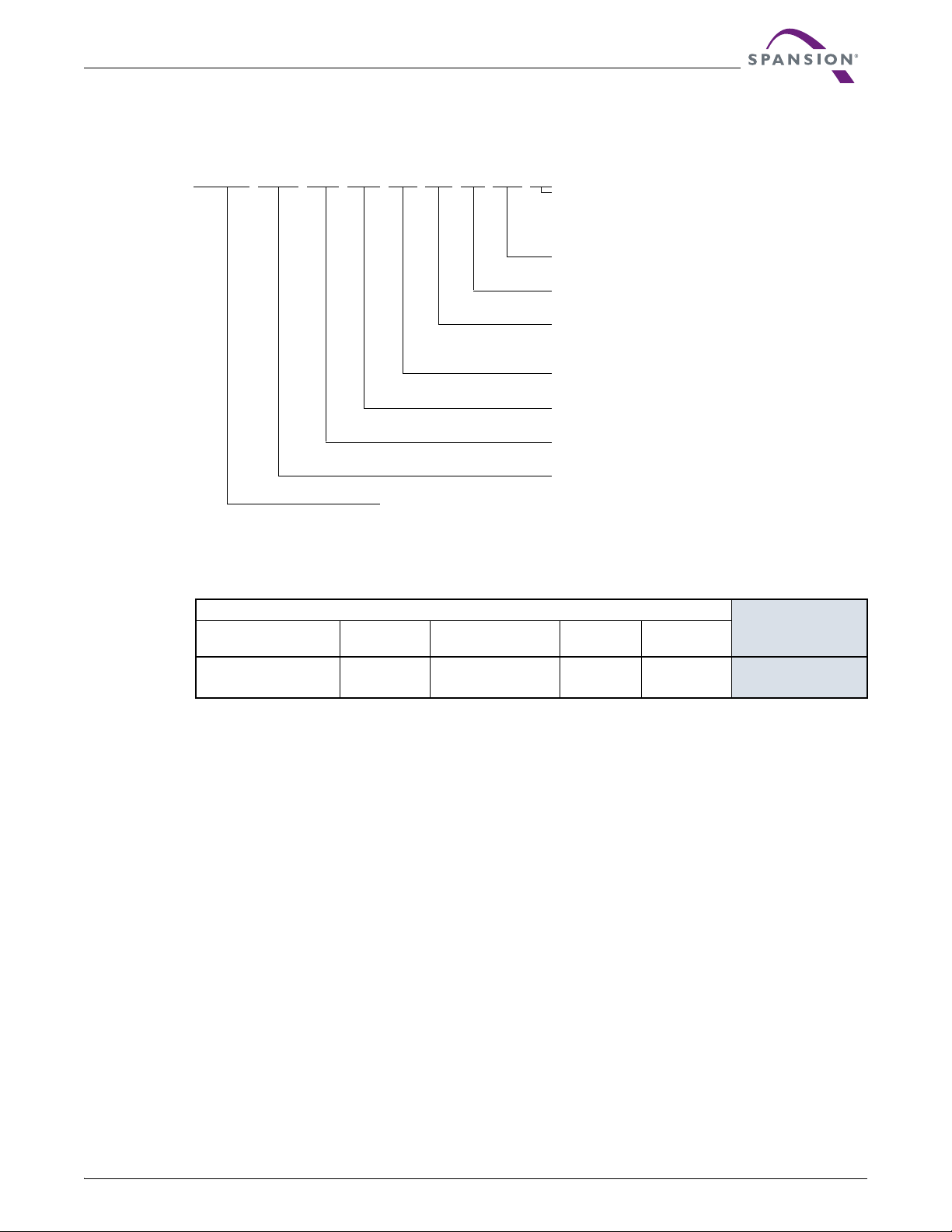
The ordering part number is formed by a valid combination of the following:
Data Sheet
S25FL 032 A 0L M A I 00 1
DEVICE FAMILY
S25FL
Spansion
TM
Memory 3.0 Volt-only, Serial Peripheral Interface (SPI) Flash Memory
PACKING TYPE (Note 1)
0 = Tray
1 = Tube
3 = 13” Tape and Reel
MODEL NUMBER (Additional Ordering Options)
00 = No additional ordering options
TEMPERATURE RANGE
I = Industrial (–40°C to + 85°C)
PACKAGE MATERIALS
A = Standard
F = Lead (Pb)-free
PACKAGE TYPE
M = 16-pin SO package
SPEED
0L = 50 MHz
DEVICE TECHNOLOGY
A = 0.20 µm MirrorBit
DENSITY
032 = 32 Mbit
Table 5.1 S25FL032A Valid Combinations Table
S25FL032A Valid Combinations
Base Ordering
Part Number Speed Option
S25FL032A 0L MAI, MFI 00 1, 3 (Note 1)
Notes
1. Contact your local sales office for availability.
2. Package marking omits leading “S25” and speed, package, and model number form.
3. A for standard package (non-Pb free); F for Pb-free package.
Packag e &
Temperature
Model
Number Packing Type
®
Process Technology
Package Marking
FL032A + (Temp) +
(Note 2)
(Note 3)
5.1 Valid Combinations
Table 5.1 lists the valid combinations configurations planned to be supported in volume for this device.
July 2, 2007 S25FL032A_00_C2 S25FL032A 9
Page 10
6. Spansion SPI Modes
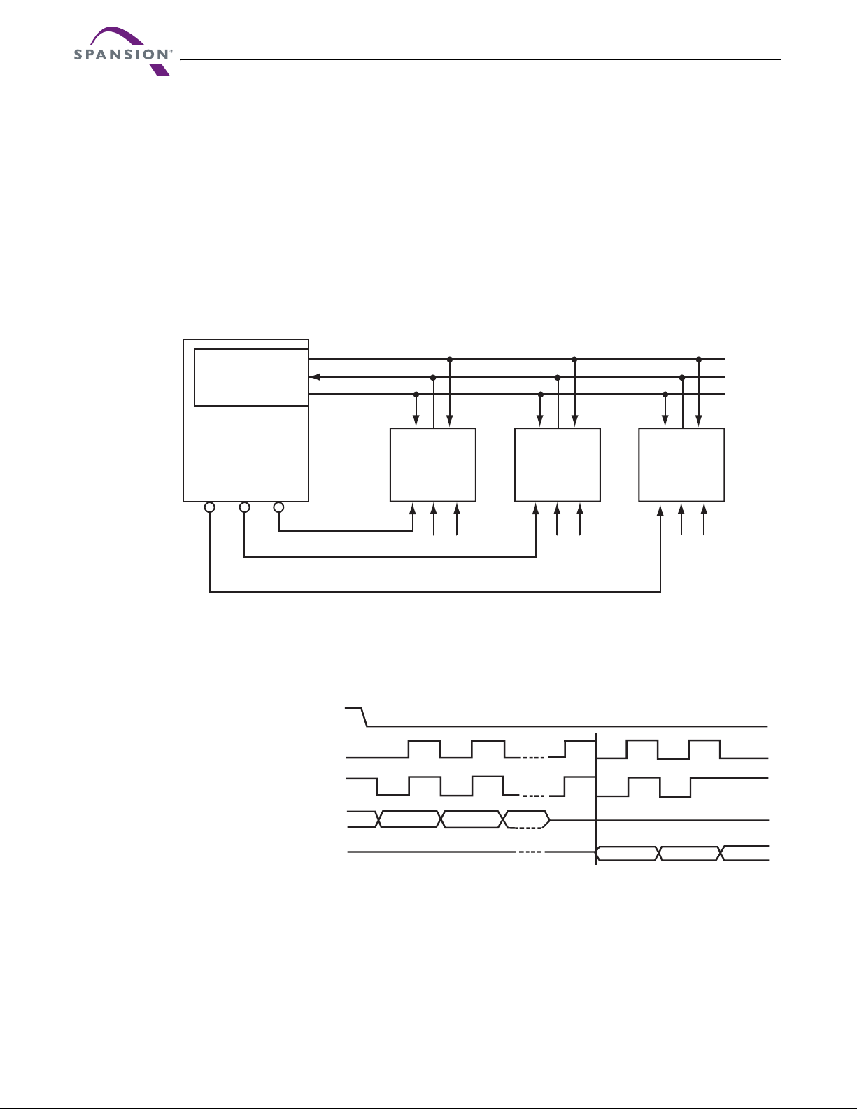
A microcontroller can use either of its two SPI modes to control Spansion SPI Flash memory devices:
CPOL = 0, CPHA = 0 (Mode 0)
CPOL = 1, CPHA = 1 (Mode 3)
Input data is latched in on the rising edge of SCK, and output data is available from the falling edge of SCK for
both modes.
When the bus master is in standby mode, SCK is as shown in Figure 6.2 for each of the two modes:
SCK remains at 0 for (CPOL = 0, CPHA = 0 Mode 0)
SCK remains at 1 for (CPOL = 1, CPHA = 1 Mode 3)
Data Sheet
Figure 6.1 Bus Master and Memory Devices on the SPI Bus
SPI Interface with
(CPOL, CPHA) =
(0, 0) or (1, 1)
Bus Master
CS3 CS2CS1
Note
The Write Protect (W#) and Hold (HOLD#) signals should be driven high (logic level 1) or low (logic level 0) as appropriate.
SO
SI
SCK
SCK SO SI SCK SO SI SCK SO SI
SPI Memory
Device
SPI Memory
Device
SPI Memory
Device
CS# W# HOLD#CS# W# HOLD#CS# W# HOLD#
Figure 6.2 SPI Modes Supported
CS#
CPHACPOL
Mode 0
00
SCK
Mode 3
10 S25FL032A S25FL032A_00_C2 July 2, 2007
11
SCK
SI
SO
MSB
MSB
Page 11

Data Sheet
7. Device Operations
All Spansion SPI devices (S25FL-A) accept and output data in bytes (8 bits at a time).
7.1 Byte or Page Programming
Programming data requires two commands: Write Enable (WREN), which is one byte, and a Page Program
(PP) sequence, which consists of four bytes plus data. The Page Program sequence accepts from 1 byte up
to 256 consecutive bytes of data (which is the size of one page) to be programmed in one operation.
Programming means that bits can either be left at 0, or programmed from 1 to 0. Changing bits from 0 to 1
requires an erase operation. Before this can be applied, the bytes of the memory need to be first erased to all
1’s (FFh) before any programming.
7.2 Sector Erase / Bulk Erase
The Sector Erase (SE) and Bulk Erase (BE) commands set all the bits in a sector or the entire memory array
to 1. While bits can be individually programmed from a 1 to 0, erasing bits from 0 to 1 must be done on a
sector-wide (SE) or array-wide (BE) level.
7.3 Monitoring Write Operations Using the Status Register
The host system can determine when a Write Status Register, program, or erase operation is complete by
monitoring the Write in Progress (WIP) bit in the Status Register. The Read from Status Register command
provides the state of the WIP bit.
7.4 Active Power and Standby Power Modes
The device is enabled and in the Active Power mode when Chip Select (CS#) is Low. When CS# is high, the
device is disabled, but may still be in the Active Power mode until all program, erase, and Write Status
Register operations have completed. The device then goes into the Standby Power mode, and power
consumption drops to I
inadvertent signals. After writing the DP command, the device ignores any further program or erase
commands, and reduces its power consumption to I
. The Deep Power Down (DP) command provides additional data protection against
SB
DP
7.5 Status Register
The Status Register contains the status and control bits that can be read or set by specific commands
(Table 9.2, S25FL032A Status Register on page 20):
Write In Progress (WIP): Indicates whether the device is performing a Write Status Register, program or
erase operation.
Write Enable Latch (WEL): Indicates the status of the internal Write Enable Latch.
Block Protect (BP2, BP1, BP0): Non-volatile bits that define memory area to be software-protected
against program and erase commands.
Status Register Write Disable (SRWD): Places the device in the Hardware Protected mode when this bit
is set to 1 and the W# input is driven low. In this mode, the non-volatile bits of the Status Register (SRWD,
BP2, BP1, BP0) become read-only bits.
.
July 2, 2007 S25FL032A_00_C2 S25FL032A 11
Page 12
7.6 Data Protection Modes
Spansion SPI Flash memory devices provide the following data protection methods:
The Write Enable (WREN) command: Must be written prior to any command that modifies data. The
WREN command sets the Write Enable Latch (WEL) bit. The WEL bit resets (disables writes) on power-up
or after the device completes the following commands:
– Page Program (PP)
– Sector Erase (SE)
– Bulk Erase (BE)
– Write Disable (WRDI)
– Write Status Register (WRSR)
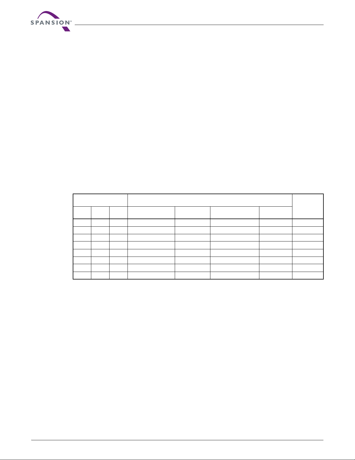
Software Protected Mode (SPM): The Block Protect (BP2, BP1, BP0) bits define the section of the
memory array that can be read but not programmed or erased. Table 7.1 shows the sizes and address
ranges of protected areas that are defined by Status Register bits BP2:BP0.
Hardware Protected Mode (HPM): The Write Protect (W#) input and the Status Register Write Disable
(SRWD) bit together provide write protection.
Clock Pulse Count: The device verifies that all program, erase, and Write Status Register commands
consist of a clock pulse count that is a multiple of eight before executing them.
Data Sheet
Table 7.1 S25FL032A Protected Area Sizes
Status Register
Block Protect Bits Memory Array
Protected
Address Range
0 0 0 None (0) 000000h–3FFFFFh SA63:SA0 0
0 0 1 3F0000h–3FFFFFh (1) SA63 000000h–3EFFFFh SA62:SA0 1/64
0 1 0 3E0000h–3FFFFFh (2) SA63:SA62 000000h–3DFFFFh SA61:SA0 1/32
0 1 1 3C0000h–3FFFFFh (4) SA63:SA60 000000h–3BFFFFh SA59:SA0 1/16
1 0 0 380000h–3FFFFFh (8) SA63:SA56 000000h–37FFFFh SA55:SA0 1/8
1 0 1 300000h–3FFFFFh (16) SA63:SA48 000000h–2FFFFFh SA47:SA0 1/4
1 1 0 200000h–3FFFFFh (32) SA63:SA32 000000h–1FFFFFh SA31:SA0 1/2
1 1 1 000000h–3FFFFFh (64) SA63:SA0 None None All
Protected
Sectors
Unprotected
Address Range
Unprotected
Sectors
Protected
Portion of
Total Memory
AreaBP2 BP1 BP0
12 S25FL032A S25FL032A_00_C2 July 2, 2007
Page 13
7.7 Hold Mode (HOLD#)
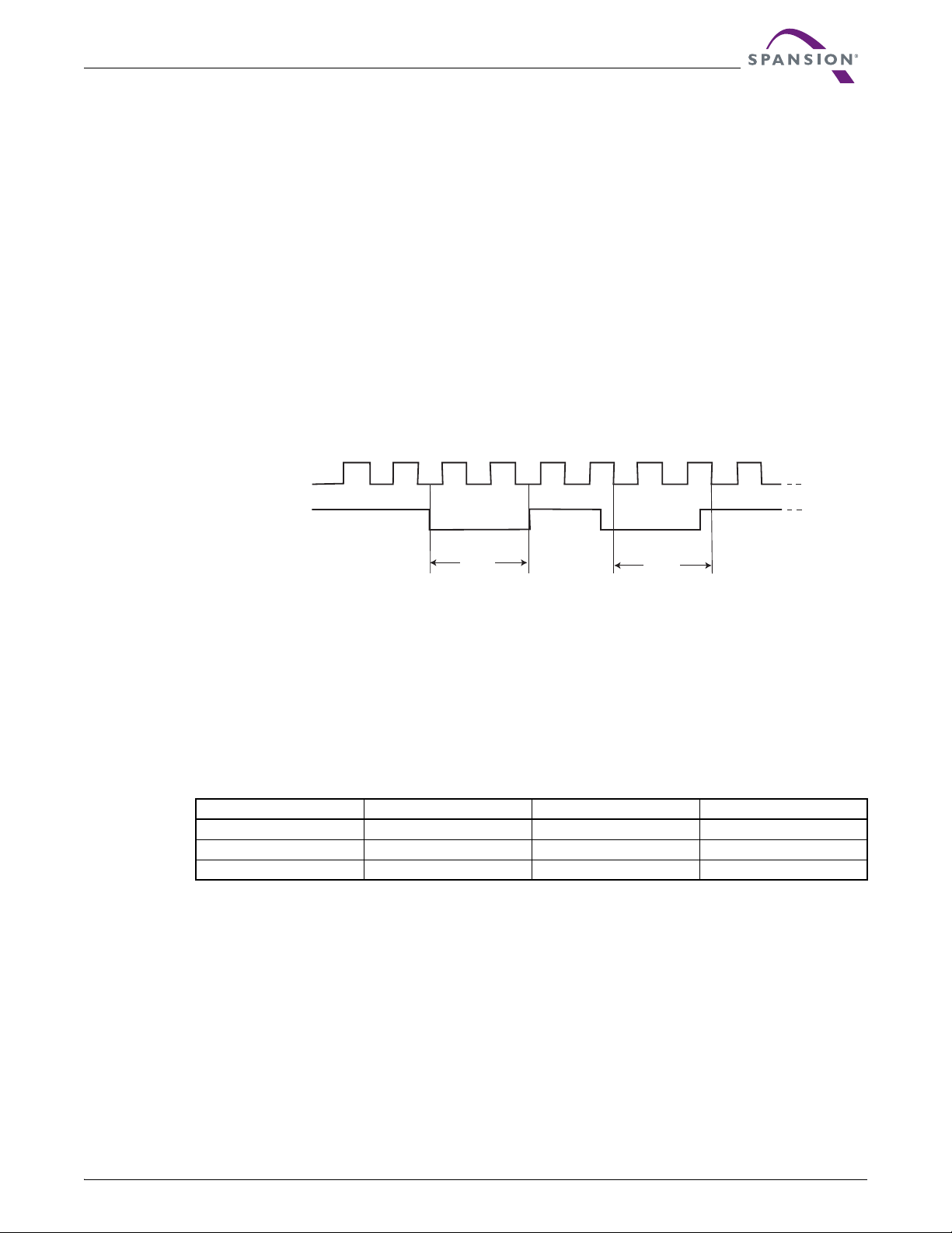
The Hold input (HOLD#) stops any serial communication with the device, but does not terminate any Write
Status Register, program or erase operation that is currently in progress.
The Hold mode starts on the falling edge of HOLD# if SCK is also low (see Figure 7.1, standard use). If the
falling edge of HOLD# does not occur while SCK is low, the Hold mode begins after the next falling edge of
SCK (non-standard use).
The Hold mode ends on the rising edge of HOLD# signal (standard use) if SCK is also low. If the rising edge
of HOLD# does not occur while SCK is low, the Hold mode ends on the next falling edge of CLK (nonstandard use) See Figure 7.1.
The SO output is high impedance, and the SI and SCK inputs are ignored (don’t care) for the duration of the
Hold mode.
CS# must remain low for the entire duration of the Hold mode to ensure that the device internal logic remains
unchanged. If CS# goes high while the device is in the Hold mode, the internal logic is reset. To prevent the
device from reverting to the Hold mode when device communication is resumed, HOLD# must be held high,
followed by driving CS# low.
SCK
Data Sheet
Figure 7.1 Hold Mode Operation
HOLD#
8. Sector Address Table
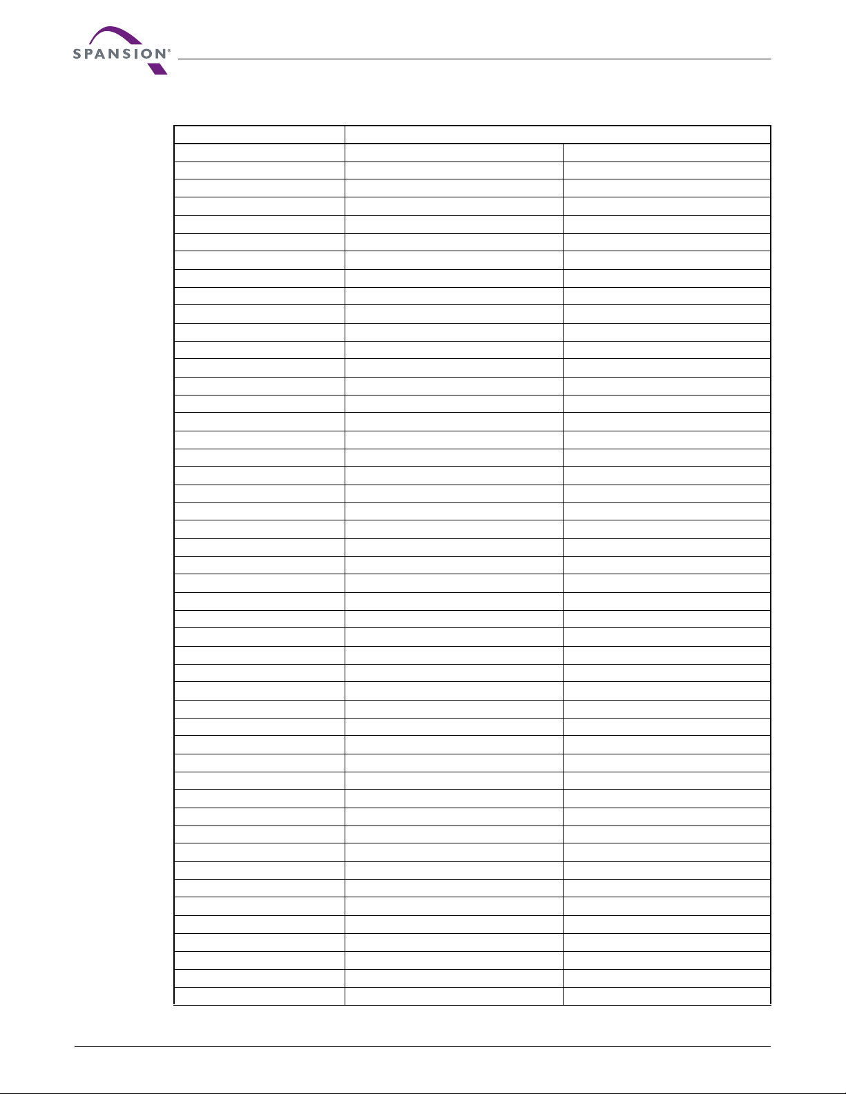
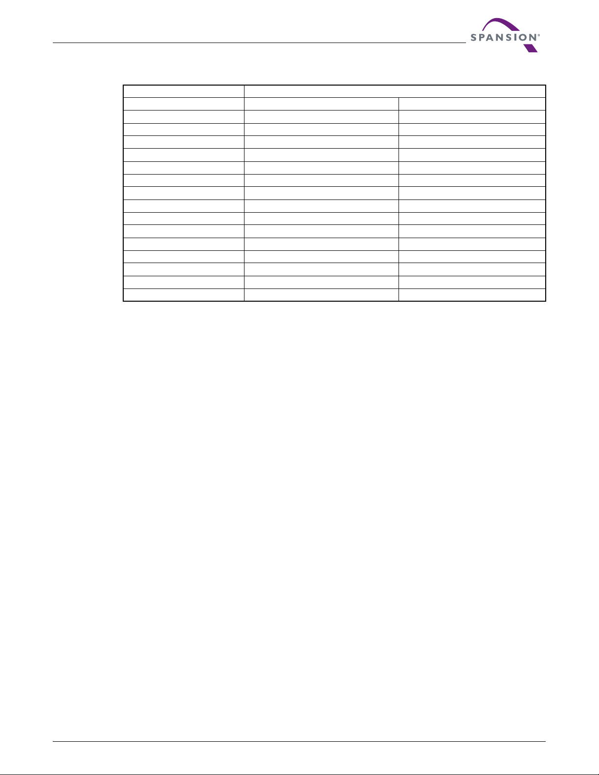
Table 8.1 shows the size of the memory array, sectors, and pages. The device uses pages to cache the
program data before the data is programmed into the memory array. Each page or byte can be individually
programmed (bits are changed from 1 to 0). The data is erased (bits are changed from 0 to 1) on a sector- or
device-wide basis using the SE or BE commands. Table 8.2 shows the starting and ending address for each
sector. The complete set of sectors comprises the memory array of the Flash device.
Each Device has Each Sector has Each Page has
4,194,304 65,536 256 bytes
16,384 256 — pages
64 — — sectors
Hold
Condition
(standard use)
Hold
Condition
(non-standard use)
Table 8.1 S25FL032A Device Organization
July 2, 2007 S25FL032A_00_C2 S25FL032A 13
Page 14
Data Sheet
Table 8.2 S25FL032A Sector Address Table (Sheet 1 of 2)
Sector Address Range
SA63 3F0000h 3FFFFFh
SA62 3E0000h 3EFFFFh
SA61 3D0000h 3DFFFFh
SA60 3C0000h 3CFFFFh
SA59 3B0000h 3BFFFFh
SA58 3A0000h 3AFFFFh
SA57 390000h 39FFFFh
SA56 380000h 38FFFFh
SA55 370000h 37FFFFh
SA54 360000h 36FFFFh
SA53 350000h 35FFFFh
SA52 340000h 34FFFFh
SA51 330000h 33FFFFh
SA50 320000h 32FFFFh
SA49 310000h 31FFFFh
SA48 300000h 30FFFFh
SA47 2F0000h 2FFFFFh
SA46 2E0000h 2EFFFFh
SA45 2D0000h 2DFFFFh
SA44 2C0000h 2CFFFFh
SA43 2B0000h 2BFFFFh
SA42 2A0000h 2AFFFFh
SA41 290000h 29FFFFh
SA40 280000h 28FFFFh
SA39 270000h 27FFFFh
SA38 260000h 26FFFFh
SA37 250000h 25FFFFh
SA36 240000h 24FFFFh
SA35 230000h 23FFFFh
SA34 220000h 22FFFFh
SA33 210000h 21FFFFh
SA32 200000h 20FFFFh
SA31 1F0000h 1FFFFFh
SA30 1E0000h 1EFFFFh
SA29 1D0000h 1DFFFFh
SA28 1C0000h 1CFFFFh
SA27 1B0000h 1BFFFFh
SA26 1A0000h 1AFFFFh
SA25 190000h 19FFFFh
SA24 180000h 18FFFFh
SA23 170000h 17FFFFh
SA22 160000h 16FFFFh
SA21 150000h 15FFFFh
SA20 140000h 14FFFFh
SA19 130000h 13FFFFh
SA18 120000h 12FFFFh
SA17 110000h 11FFFFh
SA16 100000h 10FFFFh
14 S25FL032A S25FL032A_00_C2 July 2, 2007
Page 15
Data Sheet
Table 8.2 S25FL032A Sector Address Table (Sheet 2 of 2)
Sector Address Range
SA15 0F0000h 0FFFFFh
SA14 0E0000h 0EFFFFh
SA13 0D0000h 0DFFFFh
SA12 0C0000h 0CFFFFh
SA11 0B0000h 0BFFFFh
SA10 0A0000h 0AFFFFh
SA9 090000h 09FFFFh
SA8 080000h 08FFFFh
SA7 070000h 07FFFFh
SA6 060000h 06FFFFh
SA5 050000h 05FFFFh
SA4 040000h 04FFFFh
SA3 030000h 03FFFFh
SA2 020000h 02FFFFh
SA1 010000h 01FFFFh
SA0 000000h 00FFFFh
9. Command Definitions
The host system must shift all commands, addresses, and data in and out of the device, beginning with the
most significant bit. On the first rising edge of SCK after CS# is driven low, the device accepts the one-byte
command on SI (all commands are one byte long), most significant bit first. Each successive bit is latched on
the rising edge of SCK. Table 9.4 on page 26 lists the complete set of commands.
Every command sequence begins with a one-byte command code. The command may be followed by
address, data, both, or nothing, depending on the command. CS# must be driven high after the last bit of the
command sequence has been written.
The Read Data Bytes (READ), Read Status Register (RDSR), Read Data Bytes at Higher Speed
(FAST_READ) and Read Identification (RDID) command sequences are followed by a data output sequence
on SO. CS# can be driven high after any bit of the sequence is output to terminate the operation.
The Page Program (PP), Sector Erase (SE), Bulk Erase (BE), Write Status Register (WRSR), Write Enable
(WREN), or Write Disable (WRDI) commands require that CS# be driven high at a byte boundary, otherwise
the command is not executed. Since a byte is composed of eight bits, CS# must therefore be driven high
when the number of clock pulses after CS# is driven low is an exact multiple of eight.
The device ignores any attempt to access the memory array during a Write Status Register, program, or
erase operation, and continues the operation uninterrupted.
July 2, 2007 S25FL032A_00_C2 S25FL032A 15
Page 16
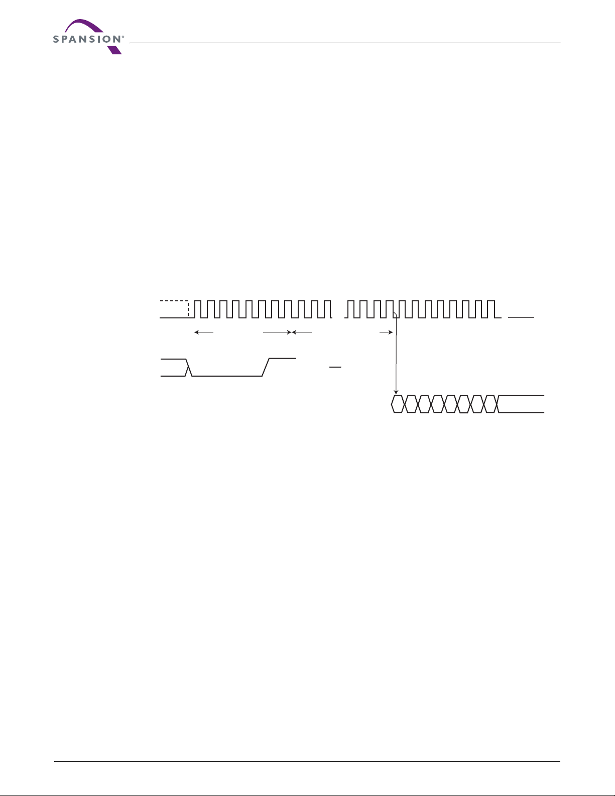
9.1 Read Data Bytes (READ)
The Read Data Bytes (READ) command reads data from the memory array at the frequency (f
at the SCK input, with a maximum speed of 33 MHz. The host system must first select the device by driving
CS# low. The READ command is then written to SI, followed by a 3-byte address (A23-A0). Each bit is
latched on the rising edge of SCK. The memory array data, at that address, are output serially on SO at a
frequency f
Figure 9.1 and Table 9.4 on page 26 detail the READ command sequence. The first byte specified can be at
any location. The device automatically increments to the next higher address after each byte of data is output.
The entire memory array can therefore be read with a single READ command. When the highest address is
reached, the address counter reverts to 00000h, allowing the read sequence to continue indefinitely.
The READ command is terminated by driving CS# high at any time during data output. The device rejects any
READ command issued while it is executing a program, erase, or Write Status Register operation, and
continues the operation uninterrupted.
, on the falling edge of SCK.
SCK
Figure 9.1 Read Data Bytes (READ) Command Sequence
Data Sheet
) presented
SCK
Hi-Z
Command 24-Bit Address
MSB
Data Out 1 Data Out 2
MSB
16 S25FL032A S25FL032A_00_C2 July 2, 2007
Page 17
Data Sheet
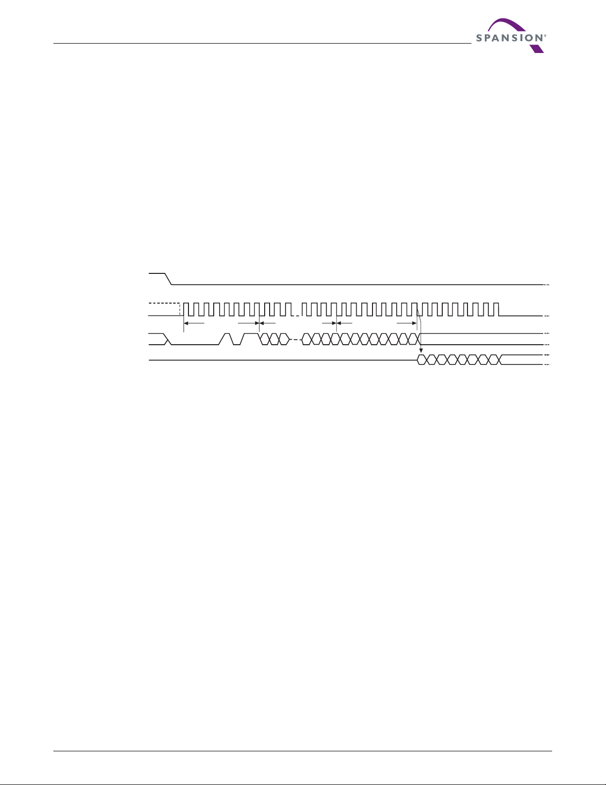
9.2 Read Data Bytes at Higher Speed (FAST_READ)
The FAST_READ command reads data from the memory array at the frequency (f
input, with a maximum speed of 50 MHz. The host system must first select the device by driving CS# low. The
FAST_READ command is then written to SI, followed by a 3-byte address (A23-A0) and a dummy byte. Each
bit is latched on the rising edge of SCK. The memory array data, at that address, are output serially on SO at
a frequency f
The FAST_READ command sequence is shown in Figure 9.2 and Table 9.4 on page 26. The first byte
specified can be at any location. The device automatically increments to the next higher address after each
byte of data is output. The entire memory array can therefore be read with a single FAST_READ command.
When the highest address is reached, the address counter reverts to 00000h, allowing the read sequence to
continue indefinitely.
The FAST_READ command is terminated by driving CS# high at any time during data output. The device
rejects any FAST_READ command issued while it is executing a program, erase, or Write Status Register
operation, and continues the operation uninterrupted.
CS#
, on the falling edge of SCK.
SCK
Figure 9.2 Read Data Bytes at Higher Speed (FAST_READ) Command Sequence
) presented at the SCK
SCK
SCK
SI
SO
Mode 3
Mode 0
Hi-Z
01 2
3 4
Command
5678
9
24-Bit Address
23
22 21
10
29 303132
28
3
2
33
35 36 37
34
38 394041
42 43
444546
47
Dummy Byte
0
1
654
7
3
210
MSB
6
7
43210
5
DATA OUT 1
MSB
7
DATA OUT 2
July 2, 2007 S25FL032A_00_C2 S25FL032A 17
Page 18
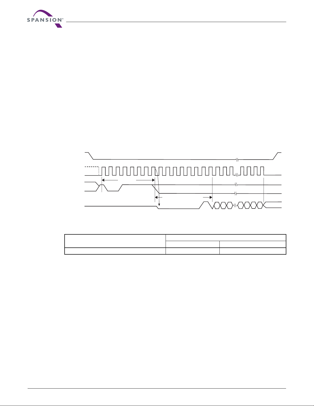
9.3 Read Identification (RDID)
The Read Identification (RDID) command outputs the one-byte manufacturer identification, followed by the
two-byte device identification, to the host system.
JEDEC assigns the manufacturer identification byte; for Spansion devices it is 01h. The device manufacturer
assigns the device identification: the first byte provides the memory type; the second byte indicates the
memory capacity. See Table 9.1 or Table 9.4 on page 26 for device ID data.
The host system must first select the device by driving CS# low. The RDID command is then written to SI,
and each bit is latched on the rising edge of SCK. The 24-bit device identification data is output from the
memory array on SO at a frequency f
The RDID command sequence is shown in Figure 9.3 and Table 9.4 on page 26.
Driving CS# high after the device identification data has been read at least once terminates the READ_ID
command. Driving CS# high at any time during data output also terminates the RDID operation.
The device rejects any RDID command issued while it is executing a program, erase, or Write Status Register
operation, and continues the operation uninterrupted.
Figure 9.3 Read Identification (RDID) Command Sequence and Data-Out Sequence
CS#
Data Sheet
, on the falling edge of SCK.
SCK
SCK
SI
SO
1
Mode 3
Mode 0
Hi-Z
2
0
Table 9.1 Read Identification (RDID) Data-Out Sequence
Manufacturer Identification
01h 02h 15h
3
Command
456
7
9
10
8
Manufacturer Identification
MSB
30
28
29
11
Memory Type Memory Capacity
14 15 16
13
12
Device Identification
18
17
Device Identification
14
13
15
3
31
0
1
2
18 S25FL032A S25FL032A_00_C2 July 2, 2007
Page 19
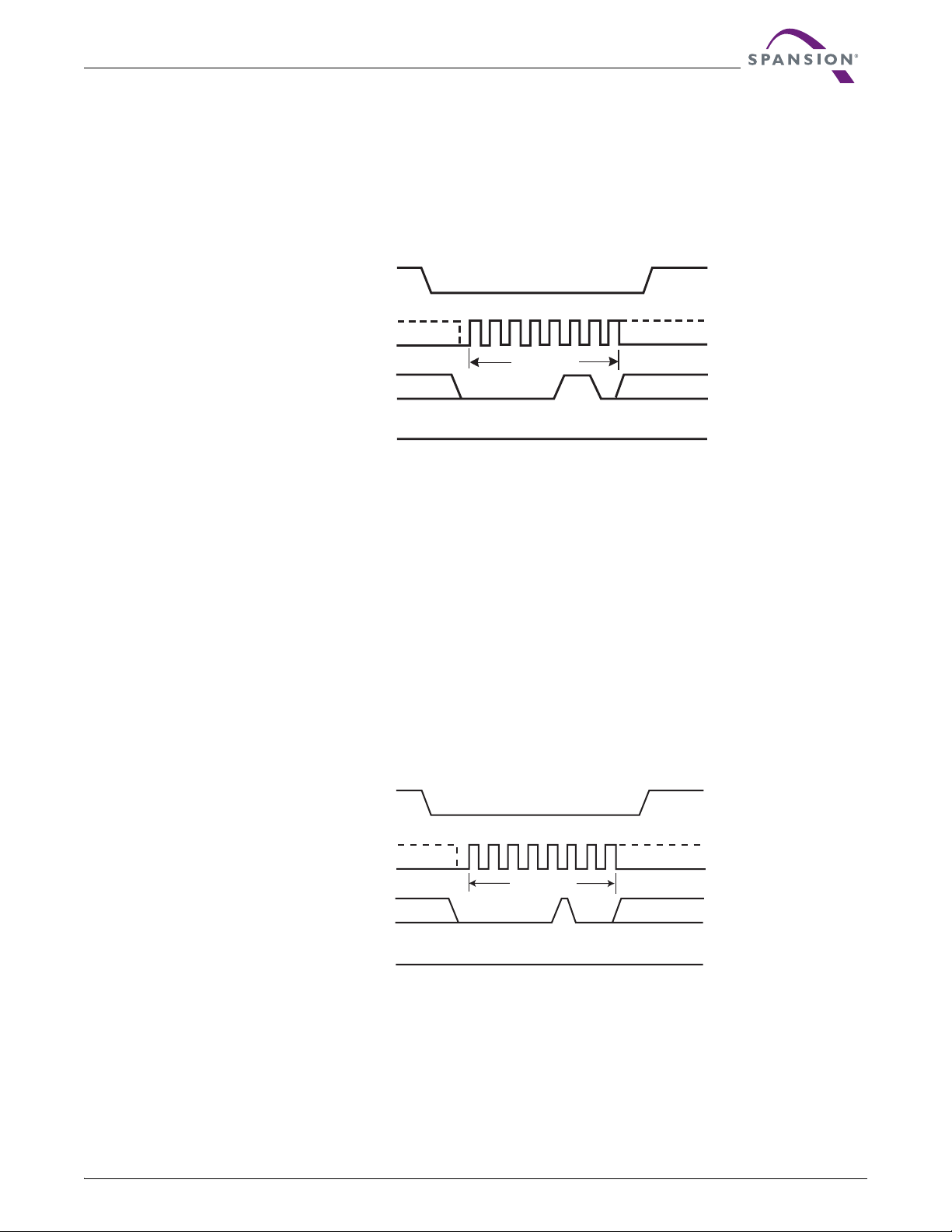
9.4 Write Enable (WREN)
The Write Enable (WREN) command (see Figure 9.4) sets the Write Enable Latch (WEL) bit to a 1, which
enables the device to accept a Write Status Register, program, or erase command. The WEL bit must be set
prior to every Page Program (PP), Erase (SE or BE) and Write Status Register (WRSR) command.
The host system must first drive CS# low, write the WREN command, and then drive CS# high.
Data Sheet
Figure 9.4 Write Enable (WREN) Command Sequence
CS#
9.5 Write Disable (WRDI)
The Write Disable (WRDI) command (see Figure 9.5) resets the Write Enable Latch (WEL) bit to a 0, which
disables the device from accepting a Write Status Register, program, or erase command. The host system
must first drive CS# low, write the WRDI command, and then drive CS# high.
Any of following conditions resets the WEL bit:
Power-up
Write Disable (WRDI) command completion
Write Status Register (WRSR) command completion
Page Program (PP) command completion
Sector Erase (SE) command completion
Bulk Erase (BE) command completion
SCK
SI
SO
Mode 3
Mode 0
Hi-Z
01 23 45
Command
67
Figure 9.5 Write Disable (WRDI) Command Sequence
CS#
7
6
5
SCK
Mode 3
Mode 0
0
3 4
1
2
Command
SI
Hi-Z
SO
July 2, 2007 S25FL032A_00_C2 S25FL032A 19
Page 20
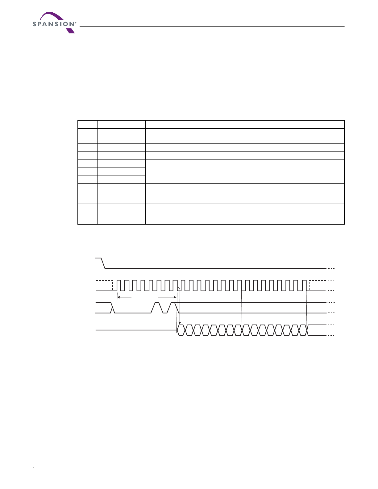
9.6 Read Status Register (RDSR)
The Read Status Register (RDSR) command outputs the state of the Status Register bits. Table 9.2 shows
the status register bits and their functions.
The RDSR command may be written at any time, even while a program, erase, or Write Status Register
operation is in progress. The host system should check the Write In Progress (WIP) bit before sending a new
command to the device if an operation is already in progress. Figure 9.6 shows the RDSR command
sequence, which also shows that it is possible to read the Status Register continuously until CS# is driven
high.
Table 9.2 S25FL032A Status Register
Bit Status Register Bit Bit Function Description
7 SRWD Status Register Write Disable
6 — — Not used
5 — — Not used
4BP2
3BP1
2BP0
1 WEL Write Enable Latch
0 WIP Write in Progress
Block Protect
Data Sheet
1 = Protects when W# is low
0 = No protection, even when W# is low
000–111 = Protects upper half of address range in 5 sizes. See
Table 7.1 on page 12.
1 = Device accepts Write Status Register, program, or erase
commands
0 = Ignores Write Status Register, program, or erase commands
1 = Device Busy. A Write Status Register, program, or erase
operation is in progress
0 = Ready. Device is in standby mode and can accept commands.
Figure 9.6 Read Status Register (RDSR) Command Sequence
CS#
SCK
Mode 3
Mode 0
0
1
432
7
6
5
8
11
9
10
12
13
14
15
Command
SI
Hi-Z
SO
6
4
2
7
MSB
Status Register Out Status Register Out
3
5
10
7
MSB
6
5
4
2
3
7
0
1
The following describes the status and control bits of the Status Register.
Write In Progress (WIP) bit: Indicates whether the device is busy performing a Write Status Register,
program, or erase operation. This bit is read-only, and is controlled internally by the device. If WIP is 1, one of
these operations is in progress; if WIP is 0, no such operation is in progress.
Write Enable Latch (WEL) bit: Determines whether the device will accept and execute a Write Status
Register, program, or erase command. When set to 1, the device accepts these commands; when set to 0,
the device rejects the commands. This bit is set to 1 by writing the WREN command, and set to 0 by the
WRDI command, and is also automatically reset to 0 after the completion of a Write Status Register, program,
or erase operation. WEL cannot be directly set by the WRSR command.
Block Protect (BP2, BP1, BP0) bits: Define the portion of the memory area that will be protected against
any changes to the stored data. The Write Status Register (WRSR) command controls these bits, which are
non-volatile. When one or more of these bits is set to 1, the corresponding memory area (see Table 7.1
20 S25FL032A S25FL032A_00_C2 July 2, 2007
Page 21

Data Sheet
on page 12) is protected against Page Program (PP) and Sector Erase (SE) commands. If the Hardware
Protected mode is enabled, BP2:BP0 cannot be changed. The Bulk Erase (BE) command is executed only if
all Block Protect (BP2, BP1, BP0) bits are 0.
Status Register Write Disable (SRWD) bit: Provides data protection when used together with the Write
Protect (W#) signal. When SRWD is set to 1 and W# is driven low, the device enters the Hardware Protected
mode. The non-volatile bits of the Status Register (SRWD, BP2, BP1, BP0) become read-only bits and the
device ignores any Write Status Register (WRSR) command.
9.7 Write Status Register (WRSR)
The Write Status Register (WRSR) command changes the bits in the Status Register. A Write Enable
(WREN) command, which itself sets the Write Enable Latch (WEL) in the Status Register, is required prior to
writing the WRSR command. Table 9.2, S25FL032A Status Register on page 20 shows the status register
bits and their functions.
The host system must drive CS# low, write the WRSR command, and the appropriate data byte on SI
(Figure 9.7).
The WRSR command cannot change the state of the Write Enable Latch (bit 1). The WREN command must
be used for that purpose. Bit 0 is a status bit controlled internally by the Flash device. Bits 6 and 5 are always
read as 0 and have no user significance.
The WRSR command also controls the value of the Status Register Write Disable (SRWD) bit. The SRWD bit
and W# together place the device in the Hardware Protected Mode (HPM). The device ignores all WRSR
commands once it enters the Hardware Protected Mode (HPM). Table 9.3 shows that W# must be driven low
and the SRWD bit must be 1 for this to occur.
Figure 9.7 Write Status Register (WRSR) Command Sequence
Table 9.3 Protection Modes
W#
Signal
Note
As defined by the values in the Block Protect (BP2, BP1, BP0) bits of the Status Register, as shown in Table 7.1 on page 12.
SRWD
Bit Mode Write Protection of the Status Register
11
10
00
01
Software
Protected
(SPM)
Hardware
Protected
(HPM)
Status Register is writable (if the WREN
command has set the WEL bit). The values in
the SRWD, BP2, BP1 and BP0 bits can be
changed.
Protected Area
(See Note)
Protected against
program and erase
commands
Unprotected Area
(See Note)
Ready to accept Page
Program and Sector
Erase commands
Table 9.3 shows that neither W# or SRWD bit by themselves can enable HPM. The device can enter HPM
either by setting the SRWD bit after driving W# low, or by driving W# low after setting the SRWD bit.
However, the device disables HPM only when W# is driven high.
Note that HPM only protects against changes to the status register. Since BP2:BP0 cannot be changed in
HPM, the size of the protected area of the memory array cannot be changed. Note that HPM provides no
protection to the memory array area outside that specified by BP2:BP0 (Software Protected Mode, or SPM).
July 2, 2007 S25FL032A_00_C2 S25FL032A 21
Page 22
If W# is permanently tied high, HPM can never be activated, and only the SPM (BP2:BP0 bits of the Status
Register) can be used.
9.8 Page Program (PP)
The Page Program (PP) command changes specified bytes in the memory array (from 1 to 0 only). A WREN
command is required prior to writing the PP command.
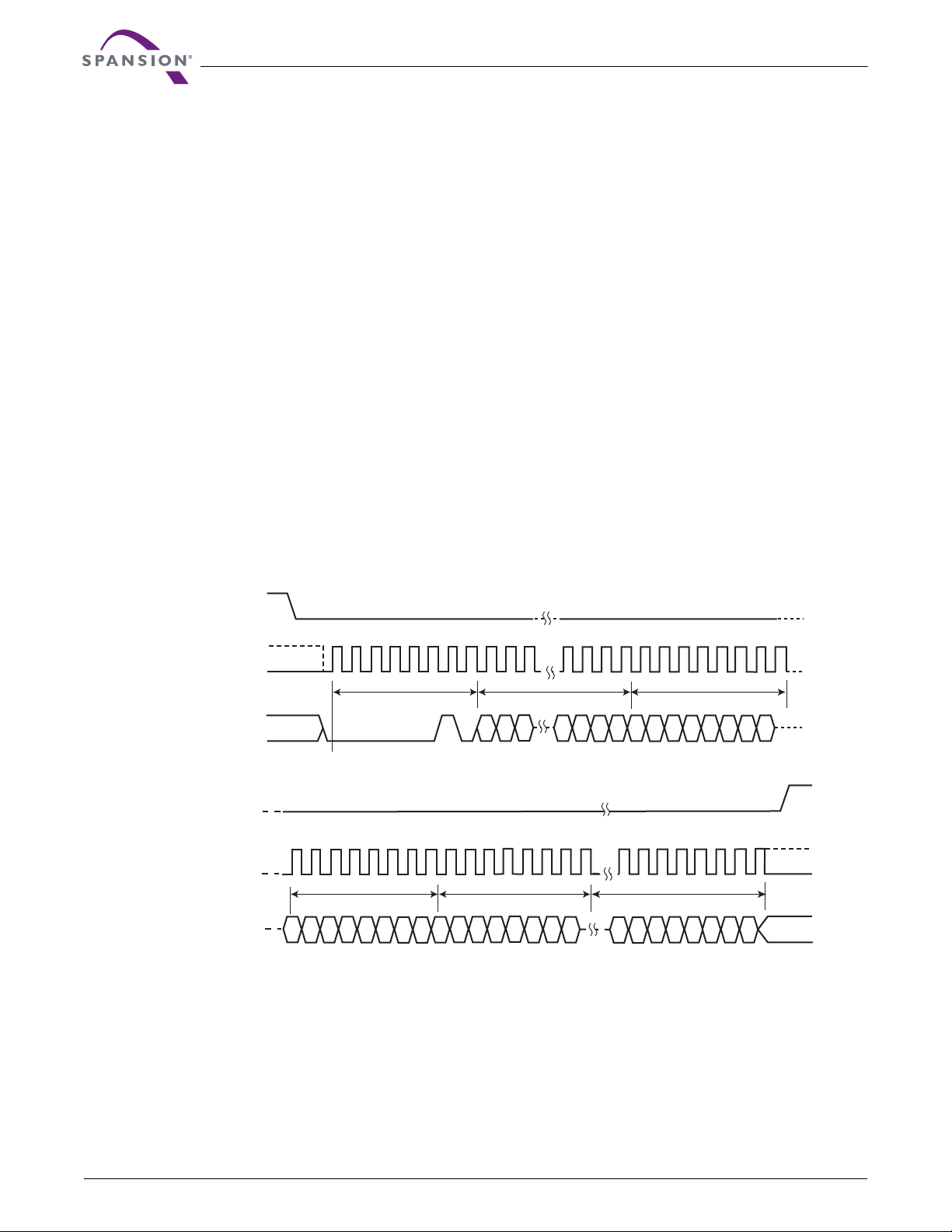
The host system must drive CS# low, and then write the PP command, three address bytes, and at least one
data byte on SI. CS# must be driven low for the entire duration of the PP sequence. The command sequence
is shown in Figure 9.8 and Table 9.4 on page 26.
The device programs only the last 256 data bytes sent to the device. If the number of data bytes exceeds this
limit, the bytes sent before the last 256 bytes are discarded, and the device begins programming the last 256
bytes sent at the starting address of the specified page. This may result in data being programmed into
different addresses within the same page than expected. If fewer than 256 data bytes are sent to device, they
are correctly programmed at the requested addresses.
The host system must drive CS# high after the device has latched the 8th bit of the data byte, otherwise the
device does not execute the PP command. The PP operation begins as soon as CS# is driven high. The
device internally controls the timing of the operation, which requires a period of t
be read to check the value of the Write In Progress (WIP) bit while the PP operation is in progress. The WIP
bit is 1 during the PP operation, and is 0 when the operation is completed. The device internally resets the
Write Enable Latch to 0 before the operation completes (the exact timing is not specified).
The device does not execute a Page Program (PP) command that specifies a page that is protected by the
Block Protect bits (BP2:BP0) (see Table 7.1 on page 12).
Data Sheet
. The Status Register may
PP
CS#
SCK
SI
CS#
SCK
SI
Mode 3
Mode 0
MSB
Figure 9.8 Page Program (PP) Command Sequence
5
4
2
0
1
3
Command
46
40
Data Byte 2 Data Byte 3
7
65
434241
432
4544
47 48
76
0
1
MSB
8
76
22
23
MSB
49 50 51
54
10
9
24-Bit Address
21
53 54 55
52
3 21
28
3
0
21
3332
313029
0765
MSB
2072
2073
Data Byte 256
7
5
6
MSB
35 36
2076
37 38 39
2
2077
34
Data Byte 1
4 3
2075
2074
4 3 210
1
0
2078
2079
22 S25FL032A S25FL032A_00_C2 July 2, 2007
Page 23
9.9 Sector Erase (SE)
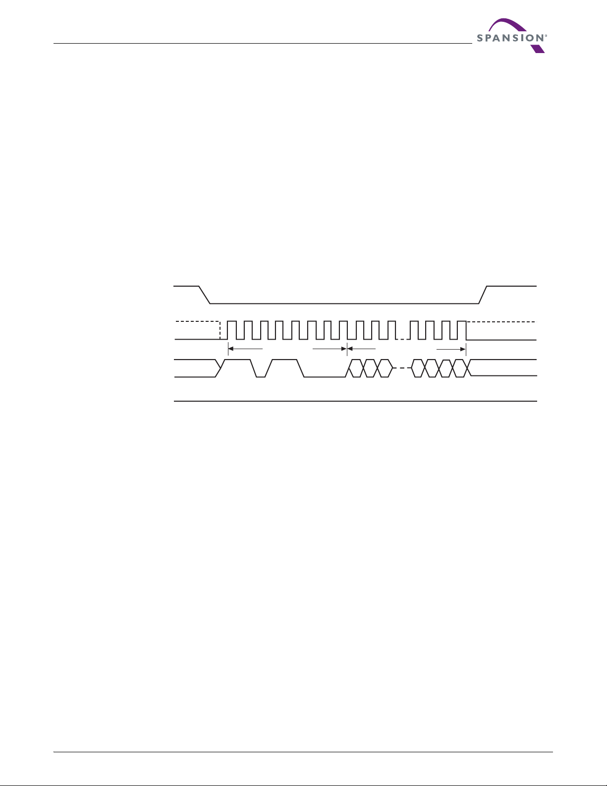
The Sector Erase (SE) command sets all bits at all addresses within a specified sector to a logic 1. A WREN
command is required prior to writing the PP command.
The host system must drive CS# low, and then write the SE command plus three address bytes on SI. Any
address within the sector (see Table 7.1 on page 12) is a valid address for the SE command. CS# must be
driven low for the entire duration of the SE sequence. The command sequence is shown in Figure 9.9 and
Table 9.4 on page 26.
The host system must drive CS# high after the device has latched the 8th bit of the SE command, otherwise
the device does not execute the command. The SE operation begins as soon as CS# is driven high. The
device internally controls the timing of the operation, which requires a period of t
be read to check the value of the Write In Progress (WIP) bit while the SE operation is in progress. The WIP
bit is 1 during the SE operation, and is 0 when the operation is completed. The device internally resets the
Write Enable Latch to 0 before the operation completes (the exact timing is not specified).
The device does not execute an SE command that specifies a sector that is protected by the Block Protect
bits (BP2:BP0) (see Table 7.1 on page 12).
CS#
Data Sheet
Figure 9.9 Sector Erase (SE) Command Sequence
. The Status Register may
SE
Mode 3
SCK
Mode 0
SI
Hi-Z
SO
9.10 Bulk Erase (BE)
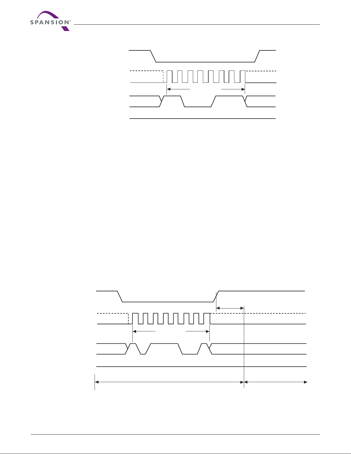
The Bulk Erase (BE) command sets all the bits within the entire memory array to logic 1s. A WREN command
is required prior to writing the PP command.
The host system must drive CS# low, and then write the BE command on SI. CS# must be driven low for the
entire duration of the BE sequence. The command sequence is shown in Figure 9.10 and Table 9.4
on page 26.
The host system must drive CS# high after the device has latched the 8th bit of the CE command, otherwise
the device does not execute the command. The BE operation begins as soon as CS# is driven high. The
device internally controls the timing of the operation, which requires a period of t
be read to check the value of the Write In Progress (WIP) bit while the BE operation is in progress. The WIP
bit is 1 during the BE operation, and is 0 when the operation is completed. The device internally resets the
Write Enable Latch to 0 before the operation completes (the exact timing is not specified).
The device only executes a BE command if all Block Protect bits (BP2:BP0) are 0 (see Table 7.1
on page 12). Otherwise, the device ignores the command.
01
2 3 45 678 910 28 29 30 31
Command 24-bit Address
23 22 21 3 2
MSB
1
. The Status Register may
BE
0
July 2, 2007 S25FL032A_00_C2 S25FL032A 23
Page 24
CS#
Data Sheet
Figure 9.10 Bulk Erase (BE) Command Sequence
Mode 3
SCK
Mode 0
SI
Hi-Z
SO
9.11 Deep Power Down (DP)
The Deep Power Down (DP) command provides the lowest power consumption mode of the device. It is
intended for periods when the device is not in active use, and ignores all commands except for the Release
from Deep Power Down (RES) command. The DP mode therefore provides the maximum data protection
against unintended write operations. The standard standby mode, which the device goes into automatically
when CS# is high (and all operations in progress are complete), should generally be used for the lowest
power consumption when the quickest return to device activity is required.
The host system must drive CS# low, and then write the DP command on SI. CS# must be driven low for the
entire duration of the DP sequence. The command sequence is shown in Figure 9.11 and Table 9.4
on page 26.
The host system must drive CS# high after the device has latched the 8th bit of the DP command, otherwise
the device does not execute the command. After a delay of t
reduces from I
Once the device has entered the DP mode, all commands are ignored except the RES command (which
releases the device from the DP mode). The RES command also provides the Electronic Signature of the
device to be output on SO, if desired (see Section 9.12 and 9.12.1).
DP mode automatically terminates when power is removed, and the device always powers up in the standard
standby mode. The device rejects any DP command issued while it is executing a program, erase, or Write
Status Register operation, and continues the operation uninterrupted.
to IDP (see Table 14.1 on page 29).
SB
012 456 7
3
Command
DP,
the device enters the DP mode and current
Figure 9.11 Deep Power Down (DP) Command Sequence
CS#
t
DP
0
1
2 3 4567
Command
SCK
Mode 3
Mode 0
SI
Hi-Z
SO
Standby Mode Deep Power-down Mode
24 S25FL032A S25FL032A_00_C2 July 2, 2007
Page 25
Data Sheet
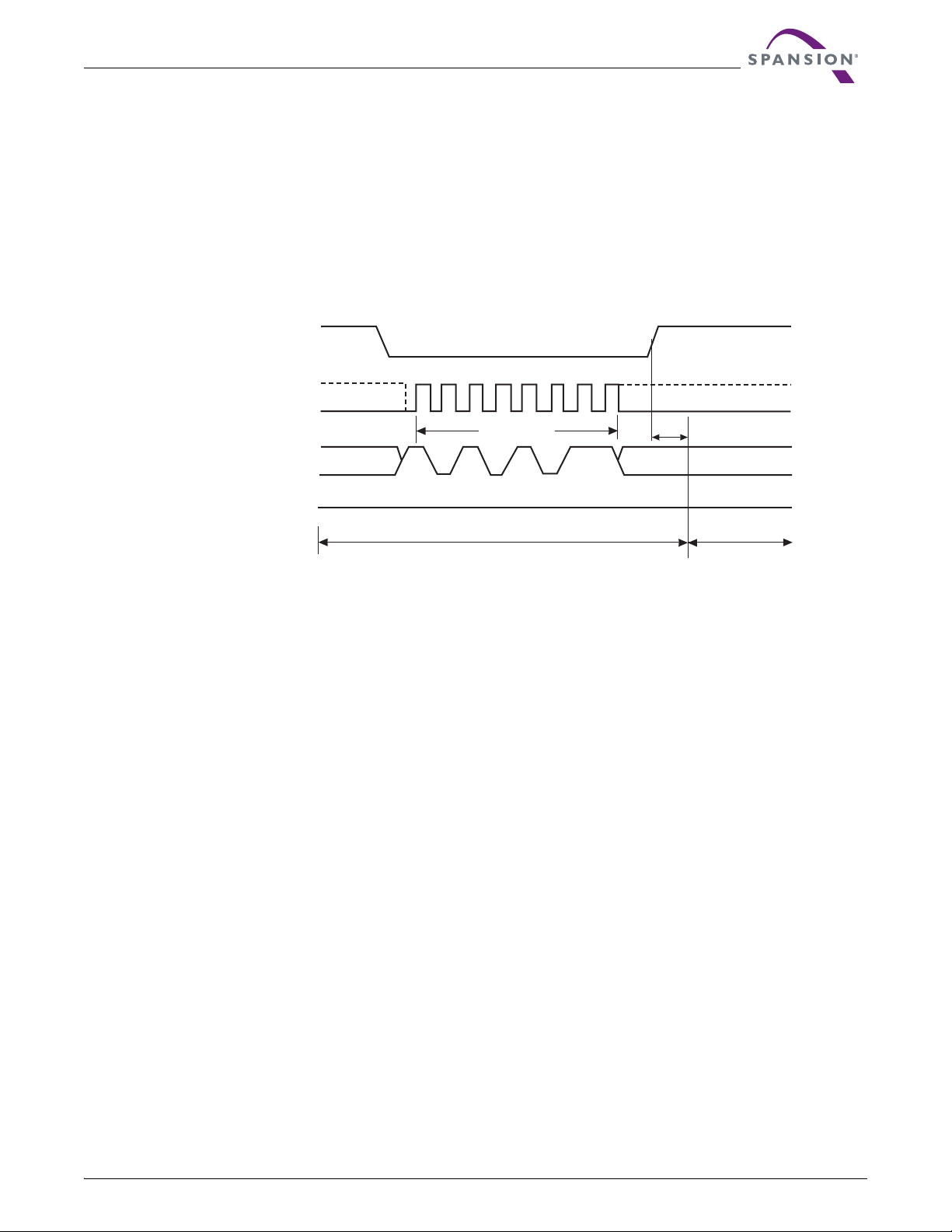
9.12 Release from Deep Power Down (RES)
The device requires the Release from Deep Power Down (RES) command to exit the Deep Power Down
mode. When the device is in the Deep Power Down mode, all commands except RES are ignored.
The host system must drive CS# low and write the RES command to SI. CS# must be driven low for the entire
duration of the sequence. The command sequence is shown in Figure 9.12 and Table 9.4 on page 26.
The host system must drive CS# high t
RES(max)
from DP mode to the standby mode after a delay of t
the device can execute any read or write command.
Figure 9.12 Release from Deep Power Down (RES) Command Sequence
CS#
after the 8-bit RES command byte. The device transitions
(see Table 16.1 on page 30). In the standby mode,
RES
7
6
t
RES
SCK
Mode 3
Mode 0
0
2 3
1
Command
5
4
SI
Hi-Z
SO
Deep Power-down Mode
Standby Mode
9.12.1 Release from Deep Power Down and Read Electronic Signature (RES)
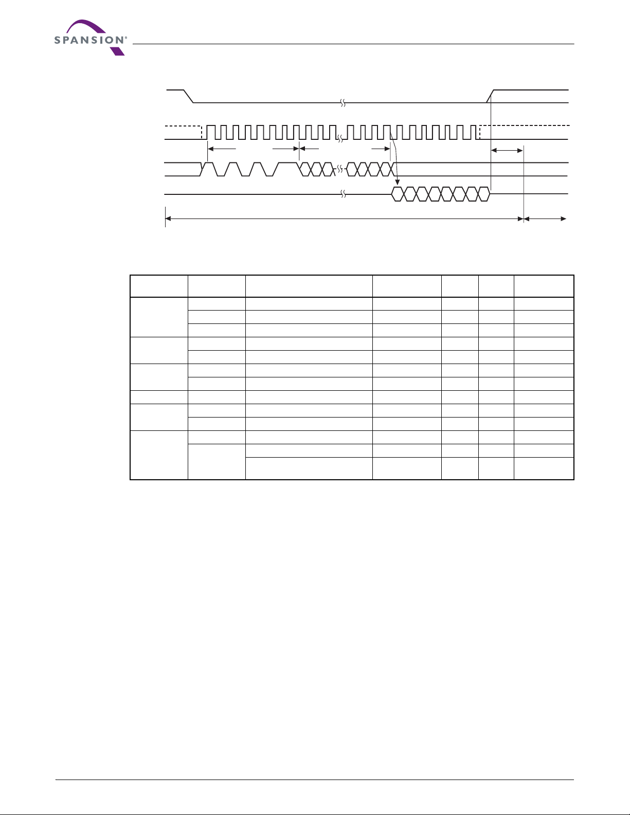
The device features an 8-bit Electronic Signature, which can be read using the RES command. See
Figure 9.13 and Table 9.4 on page 26 for the command sequence and signature value. The Electronic
Signature is not to be confused with the identification data obtained using the RDID command. The device
offers the Electronic Signature so that it can be used with previous devices that offered it; however, the
Electronic Signature should not be used for new designs, which should read the RDID data instead.
After the host system drives CS# low, it must write the RES command followed by 3 dummy bytes to SI (each
bit is latched on SI during the rising edge of SCK). The Electronic Signature is then output on SO; each bit is
shifted out on the falling edge of SCK. The RES operation is terminated by driving CS# high after the
Electronic Signature is read at least once. Additional clock cycles on SCK with CS# low cause the device to
output the Electronic Signature repeatedly.
When CS# is driven high, the device transitions from DP mode to the standby mode after a delay of t
previously described. The RES command always provides access to the Electronic Signature of the device
and can be applied even if DP mode has not been entered.
Any RES command issued while an erase, program, or WRSR operation is in progress not executed, and the
operation continues uninterrupted.
RES,
as
July 2, 2007 S25FL032A_00_C2 S25FL032A 25
Page 26
Data Sheet
Figure 9.13 Release from Deep Power Down and Read Electronic Signature (RES) Command Sequence
CS#
2
1
0
3 456 7
8
28 29 30
9
10
31 32 33 343536 37
38
SCK
t
RES
0
Standby Mode
SI
SO
Hi-Z
Command
23 22
MSB
3 Dummy Bytes
3210
21
Deep Power-down Mode
MSB
7
65
Electronic ID out
4
3 2
1
Table 9.4 Command Definitions
Operation Command Description
READ Read Data Bytes 03H (0000 0011) 3 0 1 to ∞
Read
Write Control
Erase
Program PP Page Program 02H (0000 0010) 3 0 1 to 256
Status Register
Powe r Savi ng
Notes
1. The S25FL032A has a manufacturer ID of 01h, and a device ID consisting of the memory type (02h) and the memory capacity (15h).
2. The S25FL032A has an Electronic Signature ID of 15h.
FAST_READ Read Data Bytes at Higher Speed 0BH (0000 1011) 3 1 1 to ∞
RDID Read Identification (Note 1) 9FH (1001 1111) 0 0 1 to 3
WREN Write Enable 06H (0000 0110) 0 0 0
WRDI Write Disable 04H (0000 0100) 0 0 0
SE Sector Erase D8H (1101 1000) 3 0 0
BE Bulk (Chip) Erase C7H (1100 0111) 0 0 0
RDSR Read from Status Register 05H (0000 0101) 0 0 1 to ∞
WRSR Write to Status Register 01H (0000 0001) 0 0 1
DP Deep Power Down B9H (1011 1001) 0 0 0
Release from Deep Power Down ABH (1010 1011) 0 0 0
RES
Release from Deep Power Down and
Read Electronic Signature (Note 2)
One-Byte
Command Code
ABH (1010 1011) 0 3 1 to ∞
Address
Bytes
Dummy
Byte Data Bytes
10. Power-up and Power-down
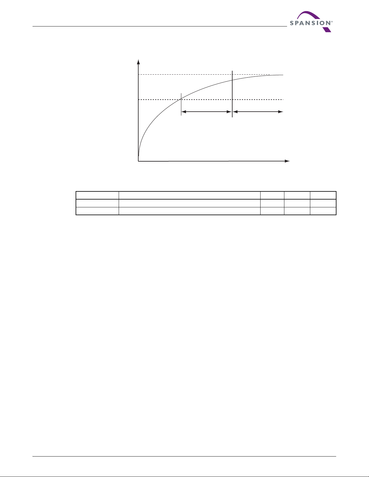
During power-up and power-down, certain conditions must be observed. CS# must follow the voltage applied
, and must not be driven low to select the device until VCC reaches the allowable values as follows
on V
CC
(see Figure 10.1 and Table 10.1 on page 27):
At power-up, VCC (min) plus a period of t
At power-down, V
SS
A pull-up resistor on Chip Select (CS#) typically meets proper power-up and power-down requirements.
No Write Status Register, program, or erase command should be sent to the device until VCC rises to the VCC
min, plus a delay of tPU. At power-up, the device is in standby mode (not Deep Power Down mode) and the
WEL bit is reset (0).
Each device in the host system should have the VCC rail decoupled by a suitable capacitor close to the
package pins (this capacitor is generally of the order of 0.1 µF), as a precaution to stabilizing the VCC feed.
When VCC drops from the operating voltage to below the minimum VCC threshold at power-down, all
operations are disabled and the device does not respond to any commands. Note that data corruption may
result if a power-down occurs while a Write Register, program, or erase operation is in progress.
26 S25FL032A S25FL032A_00_C2 July 2, 2007
PU
Page 27
Data Sheet
Vcc
(max)
V
cc
(min)
V
cc
Figure 10.1 Power-Up Timing Diagram
Symbol Parameter Min Max Unit
V
CC(min)
t
PU
11. Initial Delivery State
The device is delivered with all bits set to 1 (each byte contains FFh) upon initial factory shipment. The Status
Register contains 00h (all Status Register bits are 0).
t
PU
Full Device Access
Time
Table 10.1 Power-Up Timing Characteristics
V
(minimum) 2.7 V
CC
VCC (min) to device operation 10 ms
July 2, 2007 S25FL032A_00_C2 S25FL032A 27
Page 28
12. Absolute Maximum Ratings
Do not stress the device beyond the ratings listed in this section, or serious, permanent damage to the device
may result. These are stress ratings only and device operation at these or any other conditions beyond those
indicated in this section and in the Operating Ranges section of this document is not implied. Device
operation for extended periods at the limits listed in this section may affect device reliability.
Description Rating
Ambient Storage Temperature –65°C to +150°C
Voltage with Respect to Ground: All Inputs and I/Os –0.5 V to V
Notes
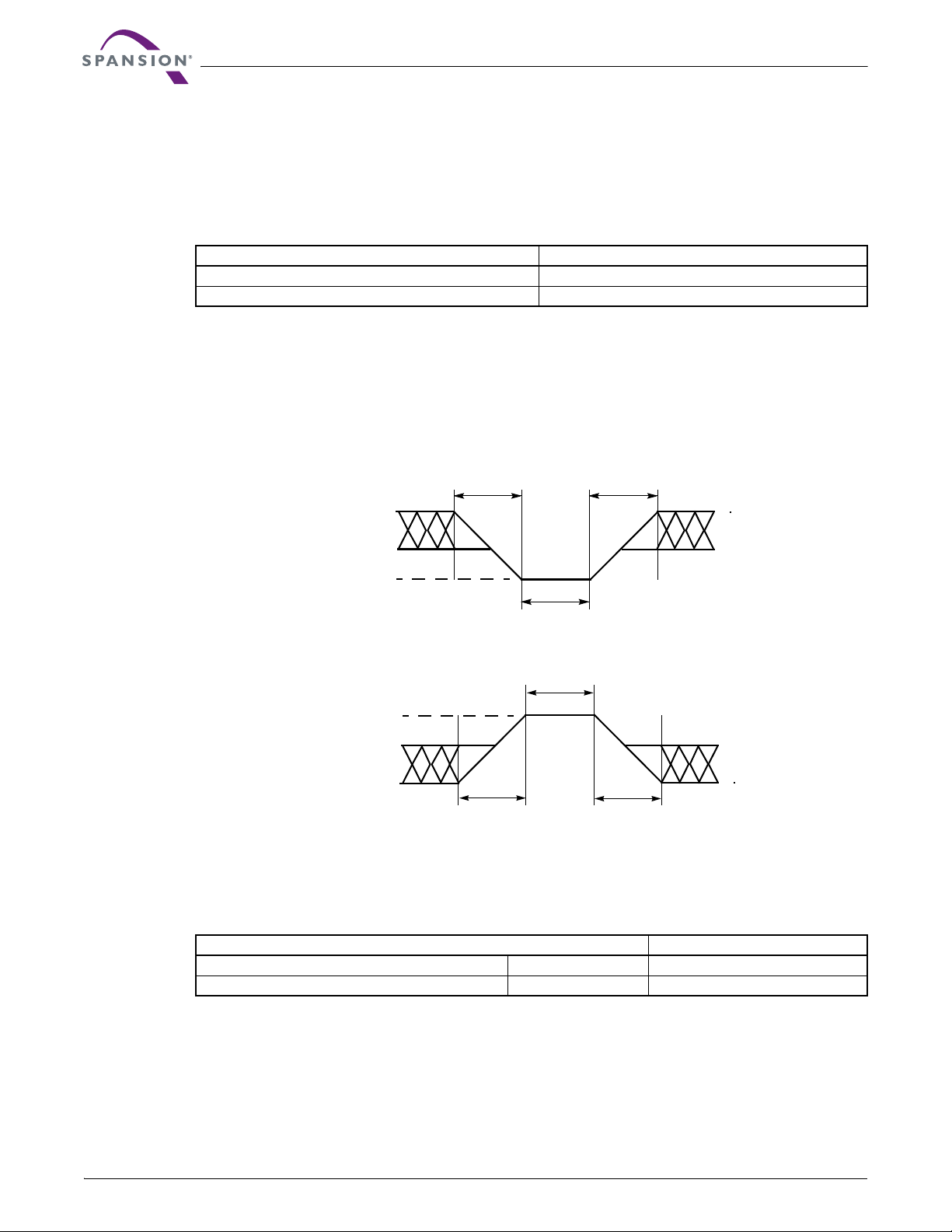
1. Minimum DC voltage on input or I/O pins is –0.5 V. During voltage transitions, inputs or I/O pins may overshoot V
of up to 20 ns. See Figure 12.1. Maximum DC voltage on output and I/O pins is 3.6 V. During voltage transitions outputs may overshoot to
V
+ 2.0 V for periods up to 20 ns. See Figure 12.2.
CC
2. No more than one output may be shorted to ground at a time. Duration of the short circuit should not be greater than one second.
3. Stresses above those listed under Absolute Maximum Ratings may cause permanent damage to the device. This is a stress rating only;
functional operation of the device at these or any other conditions above those indicated in the operational sections of this data sheet is not
implied. Exposure of the device to absolute maximum rating conditions for extended periods may affect device reliability.
Figure 12.1 Maximum Negative Overshoot Waveform
Data Sheet
Table 12.1 Absolute Maximum Ratings
20 ns
20 ns
CC
+0.5 V
to –2.0 V for periods
SS
13. Operating Ranges
Ambient Operating Temperature (T
Positive Power Supply Voltage Range 2.7 V to 3.6 V
Note
Operating ranges define those limits between which functionality of the device is guaranteed.
+0.8 V
–0.5 V
–2.0 V
20 ns
Figure 12.2 Maximum Positive Overshoot Waveform
20 ns
V
CC
+2.0 V
V
CC
+0.5 V
2.0 V
20 ns
20 ns
Table 13.1 Operating Ranges
Description Rating
) Industrial –40°C to +85°C
A
28 S25FL032A S25FL032A_00_C2 July 2, 2007
Page 29
14. DC Characteristics
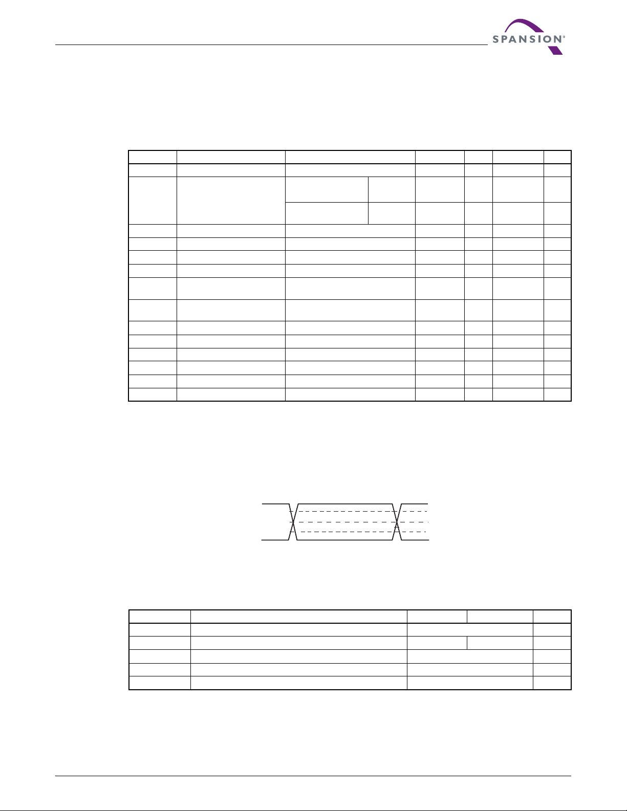
This section summarizes the DC Characteristics of the device. Designers should check that the operating
conditions in their circuit match the measurement conditions specified in the Test Specifications in Table 15.1
on page 29, when relying on the quoted parameters.
Parameter Description Test Conditions (See Note) Min Typ. Max Unit
V
I
CC1
I
CC2
I
CC3
I
CC4
I
CC5
I
I
I
V
V
V
V
Note
Typical values are at T
Supply Voltage 2.7 3 3.6 V
CC
Active Read Current
Active Page Program Current CS# = V
Active WRSR Current CS# = V
Active Sector Erase Current CS# = V
Active Bulk Erase Current CS# = V
Standby Current
SB
Deep Power Down Current
DP
Input Leakage Current VIN = GND to V
I
LI
Output Leakage Current VIN = GND to V
LO
Input Low Voltage –0.3 0.3 V
IL
Input High Voltage 0.7 V
IH
Output Low Voltage I
OL
Output High Voltage IOH = –0.1 mA V
OH
= 25°C and 3.0 V.
A
Data Sheet
Table 14.1 DC Characteristics (CMOS Compatible)
SCK = 0.1 V
SCK = 0.1 V
/0.9V
CC
CC
/0.9V
CC
CC
V
= 3.0 V
CC
CS# = V
V
= 3.0 V
CC
CS# = V
= 1.6 mA, VCC = VCC
OL
CC
CC
CC
CC
CC
CC
CC
CC
33 MHz
VCC = 3.0V
50 MHz
0.4 V
min
12 mA
19 mA
19.5 28 mA
24 mA
24 mA
24 mA
20 50 µA
1.5 5 µA
1µA
1µA
CC
CC
– 0.2 V
CC
VCC + 0.5 V
V
15. Test Conditions
Symbol Parameter Min Max Unit
C
L
0.8 V
Input Levels
0.2 V
Figure 15.1 AC Measurements I/O Waveform
CC
CC
0.7 V
0.5 V
0.3 V
CC
CC
CC
Input and Output
Timing Reference levels
Table 15.1 Test Specifications
Load Capacitance 30 pF
Input Rise and Fall Times 5 ns
Input Pulse Voltage 0.2 V
Input Timing Reference Voltage 0.3 V
Output Timing Reference Voltage 0.5 V
to 0.8 V
CC
to 0.7 V
CC
CC
CC
CC
V
V
V
July 2, 2007 S25FL032A_00_C2 S25FL032A 29
Page 30

30 S25FL032A S25FL032A_00_C2 July 2, 2007
Page 31
CS#
Data Sheet
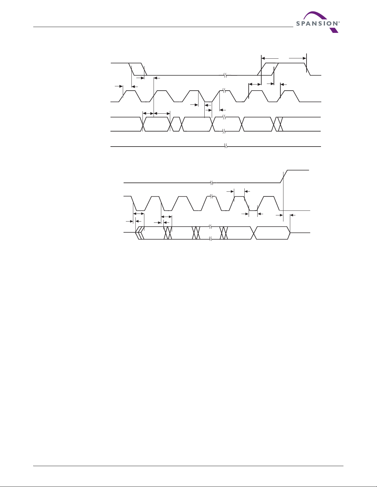
Figure 16.2 SPI Mode 0 (0,0) Input Timing
t
CS
SCK
SI
SO
Hi-Z
CS#
SCK
SO
t
CSH
t
t
SU:DAT
CSS
t
HD:DAT
MSB IN
t
CRT
t
CFT
t
CSH
LSB IN
t
CSS
Figure 16.3 SPI Mode 0 (0,0) Output Timing
t
WH
t
V
t
HO
t
V
t
HO
t
WL
LSB OUT
t
DIS
July 2, 2007 S25FL032A_00_C2 S25FL032A 31
Page 32
CS#
Data Sheet
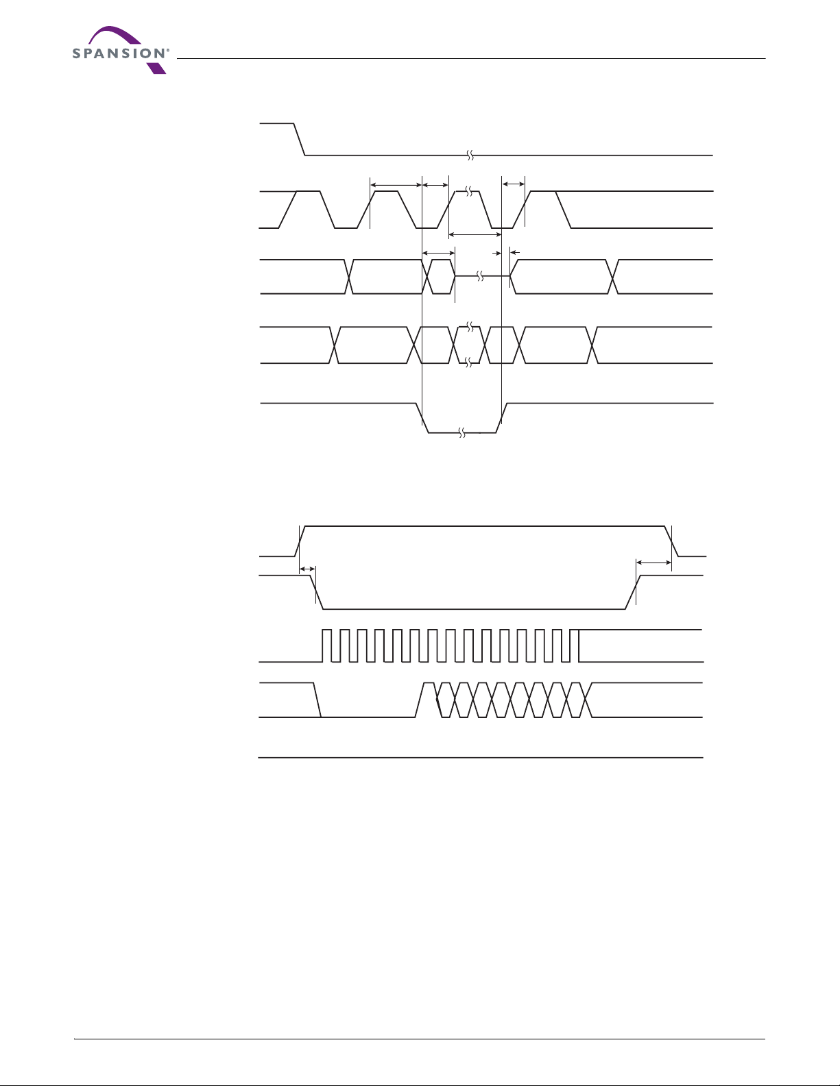
Figure 16.4 HOLD# Timing
t
HC
t
CD
t
LZ
SCK
t
t
HD
CH
t
HZ
SO
SI
HOLD#
Figure 16.5 Write Protect Setup and Hold Timing during WRSR when SRWD=1
W#
t
WPS
t
WPH
CS#
SCK
SI
SO
Hi-Z
32 S25FL032A S25FL032A_00_C2 July 2, 2007
Page 33
Data Sheet
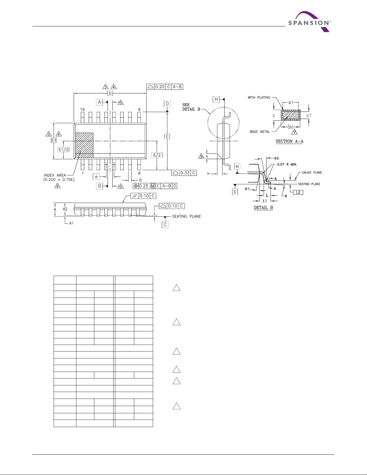
17. Physical Dimensions
17.1 SO3 016—16-pin Wide Plastic Small Outline Package (300-mil Body Width)
PACKAGE SO3 016 (inches) SO3 016 (mm)
JEDEC MS-013(D)AA MS-013(D)AA
SYMBOL MIN MAX MIN MAX
A 0.093 0.104 2.35 2.65
A1 0.004 0.012 0.10 0.30
A2 0.081 0.104 2.05 2.55
b 0.012 0.020 0.31 0.51
b1 0.011 0.019 0.27 0.48
c 0.008 0.013 0.20 0.33
c1 0.008 0.012 0.20 0.30
D 0.406 BSC 10.30 BSC
E 0.406 BSC 10.30 BSC
E1 0.295 BSC 7.50 BSC
e .050 BSC 1.27 BSC
L 0.016 0.050 0.40 1.27
L1 .055 REF 1.40 REF
L2 .010 BSC 0.25 BSC
N 16 16
h 0.10 0.30 0.25 0.75
θ 0˚ 8˚ 0˚ 8˚
θ1 5˚ 15˚ 5˚ 15˚
θ2 0˚ 0˚
NOTES:
1. ALL DIMENSIONS ARE IN BOTH INCHES AND MILLMETERS.
2. DIMENSIONING AND TOLERANCING PER ASME Y14.5M - 1994.
3. DIMENSION D DOES NOT INCLUDE MOLD FLASH,
PROTRUSIONS OR GATE BURRS. MOLD FLASH,
PROTRUSIONS OR GATE BURRS SHALL NOT EXCEED 0.15 mm
.
PER END. DIMENSION E1 DOES NOT INCLUDE INTERLEAD
FLASH OR PROTRUSION INTERLEAD FLASH OR PROTRUSION
SHALL NOT EXCEED 0.25 mm PER SIDE. D AND E1
DIMENSIONS ARE DETERMINED AT DATUM H.
4. THE PACKAGE TOP MAY BE SMALLER THAN THE PACKAGE
BOTTOM. DIMENSIONS D AND E1 ARE DETERMINED AT THE
OUTMOST EXTREMES OF THE PLASTIC BODY EXCLUSIVE OF
MOLD FLASH, TIE BAR BURRS, GATE BURRS AND INTERLEAD
FLASH. BUT INCLUDING ANY MISMATCH BETWEEN THE TOP
AND BOTTOM OF THE PLASTIC BODY.
5. DATUMS A AND B TO BE DETERMINED AT DATUM H.
6. "N" IS THE MAXIMUM NUMBER OF TERMINAL POSITIONS FOR
THE SPECIFIED PACKAGE LENGTH.
7. THE DIMENSIONS APPLY TO THE FLAT SECTION OF THE LEAD
BETWEEN 0.10 TO 0.25 mm FROM THE LEAD TIP.
8. DIMENSION "b" DOES NOT INCLUDE DAMBAR PROTRUSION.
ALLOWABLE DAMBAR PROTRUSION SHALL BE 0.10 mm TOTAL
IN EXCESS OF THE "b" DIMENSION AT MAXIMUM MATERIAL
CONDITION. THE DAMBAR CANNOT BE LOCATED ON THE
LOWER RADIUS OF THE LEAD FOOT.
9. THIS CHAMFER FEATURE IS OPTIONAL. IF IT IS NOT PRESENT,
THEN A PIN 1 IDENTIFIER MUST BE LOCATED WITHIN THE INDEX
AREA INDICATED.
10. LEAD COPLANARITY SHALL BE WITHIN 0.10 mm AS MEASURED
FROM THE SEATING PLANE.
3601 \ 16-038.03 \ 8.31.6
July 2, 2007 S25FL032A_00_C2 S25FL032A 33
Page 34

34 S25FL032A S25FL032A_00_C2 July 2, 2007
Page 35

Data Sheet
Colophon
The products described in this document are designed, developed and manufactured as contemplated for general use, including without
limitation, ordinary industrial use, general office use, personal use, and household use, but are not designed, developed and manufactured as
contemplated (1) foy i03 -1.p417 75cny use that includes3 -1.pfay itay il risks or dangers that, unless extremely high safety is secured, could have a serious3 -1.peffect to the
public, and could lead directly to death, personal injury, severe physical damage or other loss (i.e., nuclear reac in nuclear fcility,
aircraft flight control, air traffic control, mass transport control, medical life support system, missile launch control in weapon system), or (2) for
any use where chance of failure is intolerable (i.e., submersible repeater and artificial satellite). Please note that Spansion will not be liable to
you and/or any third party for any claims or damag17 75ces3arising in17 75c connection with above-mentioned uses of the products. Any semiconductor
devices hav an inherent chance of failure. You must protect agains t injury, damage or loss from such failures by incorporating safety design
measures into your facility and equipment such as redundancy, fire protection, and prevvvls and other abnormal
operating conditions. If any products described in this -1.pdocument represent -1.pgoods or technologies subject to certain restrictions on export under
the Foreign Exchange and Foreign Trade Law of Japan, the US Export Administration Regulations or the applicable laws of any other country,
the prior authorization by the respective government entity will be required for export of those products.
Trademarks and Notice
The contents of this document are subject to change without notice. This document may contain information on a Spansion product under
development by Spansion. Spansion reservthe right to change or discontinue work on any product without notice. The information in this ]TJ-57.4887 -1.2556 TD0.0003 Tc-0.0302 Tw[(document is pro)14.9(v)-3.5(ide)-7.6(d)-0.1( )7.5(as is without w)15.5(a)-0.1(rr)10(an)]TJ18.4211 0 TD[(ty or guar)10(a)-7.6(n)-0.1(tee of )7.5(an)7.4(y kind as )7.5(to)-7.6( )7.5(its )7.5(accur)10(a)-0.1(cy)94.3(, completeness)11.6(,)0.1( )7.5(o)-7.6(per)10(ability)101.8(, fitn)-7.6(ess f)30.2(o)-0.1(r)]TJ35.9248 0 TD-0.0003 Tc-0.0296 Tw[( par)-43.2(ticular pur)-28.2(p)-8.2(o)-0.7(se)14.3(, )]TJ-54.3459 -1.2481 TD0.0005 Tc-0.0379 Tw[(merchantability)94.5(, non-inf)-7.2(r)-12.4(in)-7.4(gement )-7.5(of third-par)-42.4(ty )-7.5(r)-12.4(i)-3.1(ghts)11.8(,)0.3( or an)15.1(y )-7.5(other)]TJ29.0451 0 TD0.0006 Tc-0.0305 Tw[( w)15.8(a)0.2(rr)10.3(anty)102.1(,)0.4( e)30.3(x)4.4(p)-7.3(r)2.8(ess)19.4c, implied, or statutory. Spansion assumes no liability for any
damages of any kind arising out of the use of the information in this document.
Copyright © 2005-2007 Spansion Inc. All rights reserved. Spansion
®
, the Spansion Logo, MirrorBit®, MirrorBit® Eclipse™, ORNAND™, HD-SIM™
and combinations thereof, are trademarks of Spansion LLC in the US and other countries. Other names used are for informational
July 2, 2007 S25FL032A_00_C2 S25FL032A 35
 Loading...