

Page 1

RTL8111B-GR
INTEGRATED GIGABIT ETHERNET CONTROLLER
FOR PCI EXPRESS™ APPLICATIONS
DATASHEET
Rev. 1.4
02 December 2005
Track ID: JATR-1076-21
Realtek Semiconductor Corp.
No. 2, Innovation Road II, Hsinchu Science Park, Hsinchu 300, Taiwan
Tel.: +886-3-578-0211. Fax: +886-3-577-6047
www.realtek.com.tw
Page 2

RTL8111B-GR
Datasheet
COPYRIGHT
©2005 Realtek Semiconductor Corp. All rights reserved. No part of this document may be reproduced,
transmitted, transcribed, stored in a retrieval system, or translated into any language in any form or by any
means without the written permission of Realtek Semiconductor Corp.
DISCLAIMER
Realtek provides this document “as is”, without warranty of any kind, neither expressed nor implied,
including, but not limited to, the particular purpose. Realtek may make improvements and/or changes in
this document or in the product described in this document at any time. This document could include
technical inaccuracies or typographical errors.
TRADEMARKS
Realtek is a trademark of Realtek Semiconductor Corporation. Other names mentioned in this document
are trademarks/registered trademarks of their respective owners.
USING THIS DOCUMENT
This document is intended for the software engineer’s reference and provides detailed programming
information.
Though every effort has been made to ensure that this document is current and accurate, more information
may have become available subsequent to the production of this guide. In that event, please contact your
Realtek representative for additional information that may help in the development process.
REVISION HISTORY
Revision Release Date
1.0 2005/01/17 First release.
1.1 2005/03/24 Changed Table 8, Power & Ground, page 6.
1.2 2005/06/14 Changed Figure 1, Pin Assignments, Page 3.
1.3 2005/08/17 Added ‘Exposed pad size’ information on page 24.
1.4 2005/12/02 Changed Table 5, Clock, page 5.
Summary
Added package identification information on page 3 and on page 24.
Table 4, Transceiver Interface, Page 5.
Table 11, Absolute Maximum Ratings, Page 16.
Table 12, Recommended Operating Conditions, Page 16.
Table 15, DC Characteristics, Page 17.
Removed SPI flash related items.
Removed Lead-free package information.
Added ‘Green package’ information on page 3 and on page 24.
Changed Figure 1, Pin Assignments, Page 3.
Changed Table 21 Ordering Information, page 24.
Changed Table 12, Recommended Operating Conditions, Page 16.
Changed Table 15, DC Characteristics, Page 17.
Integrated Gigabit Ethernet Controller for PCI Express ii Track ID: JATR-1076-21 Rev. 1.4
Page 3

RTL8111B-GR
Datasheet
Table of Contents
1. General Description .................................................................................................... 1
2. Features ........................................................................................................................2
3. System Applications .................................................................................................... 2
4. Pin Assignments........................................................................................................... 3
4.1. PACKAGE IDENTIFICATION ...............................................................................................................3
5. Pin Descriptions........................................................................................................... 4
5.1. POWER MANAGEMENT/ISOLATION...................................................................................................4
5.2. PCI
5.3. EEPROM.........................................................................................................................................4
5.4. T
5.5. CLOCK..............................................................................................................................................5
5.6. REGULATOR & REFERENCE..............................................................................................................5
5.7. LEDS ...............................................................................................................................................5
5.8. POWER & GROUND...........................................................................................................................6
5.9. NC (NOT CONNECTED) PINS ............................................................................................................6
EXPRESS INTERFACE .................................................................................................................4
RANSCEIVER INTERFACE ................................................................................................................5
6. Functional Description................................................................................................ 7
6.1. PCI EXPRESS BUS INTERFACE ..........................................................................................................7
6.1.1. PCI Express Transmitter.........................................................................................................................................7
6.1.2. PCI Express Receiver .............................................................................................................................................7
6.2. LED FUNCTIONS ..............................................................................................................................7
6.2.1. Link Monitor...........................................................................................................................................................7
6.2.2. Rx LED...................................................................................................................................................................8
6.2.3. Tx LED ...................................................................................................................................................................8
6.2.4. Tx/Rx LED..............................................................................................................................................................9
6.2.5. LINK/ACT LED ....................................................................................................................................................10
6.3. PHY TRANSCEIVER ........................................................................................................................11
6.3.1. PHY Transmitter ................................................................................................................................................... 11
6.3.2. PHY Receiver........................................................................................................................................................11
6.4. N
6.5. EEPROM
6.6. P
6.7. V
EXT PAGE ....................................................................................................................................12
INTERFACE ....................................................................................................................12
OWER MANAGEMENT ...................................................................................................................13
ITAL PRODUCT DATA (VPD) .......................................................................................................15
7. Characteristics ........................................................................................................... 16
7.1. ABSOLUTE MAXIMUM RATINGS .....................................................................................................16
7.2. RECOMMENDED OPERATING CONDITIONS......................................................................................16
7.3. CRYSTAL REQUIREMENTS ..............................................................................................................16
7.4. T
7.5. DC
7.6. AC CHARACTERISTICS ...................................................................................................................18
HERMAL CHARACTERISTICS .........................................................................................................17
CHARACTERISTICS ...................................................................................................................17
Integrated Gigabit Ethernet Controller for PCI Express iii Track ID: JATR-1076-21 Rev. 1.4
Page 4

RTL8111B-GR
Datasheet
7.6.1. Serial EEPROM Interface Timing ........................................................................................................................18
7.7. PCI EXPRESS BUS PARAMETERS ....................................................................................................20
7.7.1. Differential Transmitter Parameters.....................................................................................................................20
7.7.2. Differential Receiver Parameters.........................................................................................................................21
7.7.3. REFCLK Parameters............................................................................................................................................21
7.7.4. Auxiliary Signal Timing Parameters ....................................................................................................................23
8. Mechanical Dimensions ............................................................................................ 24
9. Ordering Information ............................................................................................... 24
List of Tables
Table 1. Power Management/Isolation .....................................................................................................4
Table 2. PCI Express Interface .................................................................................................................4
Table 3. EEPROM ....................................................................................................................................4
Table 4. Transceiver Interface ..................................................................................................................5
Table 5. Clock...........................................................................................................................................5
Table 6. Regulator & Reference ...............................................................................................................5
Table 7. LEDs ...........................................................................................................................................5
Table 8. Power & Ground.........................................................................................................................6
Table 9. NC (Not Connected) Pins ...........................................................................................................6
Table 10. EEPROM Interface...................................................................................................................12
Table 11. Absolute Maximum Ratings.....................................................................................................16
Table 12. Recommended Operating Conditions.......................................................................................16
Table 13. Crystal Requirements ...............................................................................................................16
Table 14. Thermal Characteristics............................................................................................................17
Table 15. DC Characteristics....................................................................................................................17
Table 16. EEPROM Access Timing Parameters ......................................................................................19
Table 17. Differential Transmitter Parameters .........................................................................................20
Table 18. Differential Receiver Parameters..............................................................................................21
Table 19. REFCLK Parameters ................................................................................................................21
Table 20. Auxiliary Signal Timing Parameters ........................................................................................23
Table 21. Ordering Information................................................................................................................24
Integrated Gigabit Ethernet Controller for PCI Express iv Track ID: JATR-1076-21 Rev. 1.4
Page 5

RTL8111B-GR
Datasheet
List of Figures
Figure 1. Pin Assignments........................................................................................................................3
Figure 2. Rx LED .....................................................................................................................................8
Figure 3. Tx LED......................................................................................................................................8
Figure 4. Tx/Rx LED................................................................................................................................9
Figure 5. LINK/ACT LED .....................................................................................................................10
Figure 6. Serial EEPROM Interface Timing ..........................................................................................18
Figure 7. REFCLK Single-Ended Measurement Points for T
Figure 8. REFCLK Single-Ended Measurement Points for V
Figure 9. REFCLK Differential Measurement Points for T
Figure 10. REFCLK V
Range .............................................................................................................23
cross
Figure 11. Auxiliary Signal Timing..........................................................................................................23
and T
rise
, V
ovs
, Duty Cycle, and Jitter .......................22
period
..............................................22
fall
and Vrb......................................22
uds,
Integrated Gigabit Ethernet Controller for PCI Express v Track ID: JATR-1076-21 Rev. 1.4
Page 6

RTL8111B-GR
Datasheet
1. General Description
The Realtek RTL8111B-GR Gigabit Ethernet controller combines a triple-speed IEEE 802.3 compliant
Media Access Controller (MAC) with a triple-speed Ethernet transceiver, PCI Express bus controller, and
embedded memory. With state-of-the-art DSP technology and mixed-mode signal technology, the
RTL8111B-GR offers high-speed transmission over CAT 5 UTP cable or CAT 3 UTP (10Mbps only)
cable. Functions such as Crossover Detection & Auto-Correction, polarity correction, adaptive
equalization, cross-talk cancellation, echo cancellation, timing recovery, and error correction are
implemented to provide robust transmission and reception capability at high speeds.
The device supports the PCI Express 1.0a bus interface for host communications with power management
and is compliant with the IEEE 802.3u specification for 10/100Mbps Ethernet and the IEEE 802.3ab
specification for 1000Mbps Ethernet. It also supports an auxiliary power auto-detect function, and will
auto-configure related bits of the PCI power management registers in PCI configuration space.
Advanced Configuration Power management Interface (ACPI)—power management for modern
operating systems that are capable of Operating System-directed Power Management (OSPM)—is
supported to achieve the most efficient power management possible. PCI Message Signaled Interrupt
(MSI) is also supported.
In addition to the ACPI feature, remote wake-up (including AMD Magic Packet™, Re-LinkOk, and
Microsoft® Wake-up frame) is supported in both ACPI and APM (Advanced Power Management)
environments. To support WOL from a deep power down state (e.g., D3cold, i.e. main power is off and
only auxiliary exists), the auxiliary power source must be able to provide the needed power for the
RTL8111B-GR.
The RTL8111B-GR is fully compliant with Microsoft® NDIS5 (IP, TCP, UDP) Checksum and
Segmentation Task-offload features, and supports IEEE 802 IP Layer 2 priority encoding and
IEEE 802.1Q Virtual bridged Local Area Network (VLAN). The above features contribute to lowering
CPU utilization, especially benefiting performance when in operation on a network server.
The device also features next-generation inter-connect PCI Express technology. PCI Express is a
high-bandwidth, low pin count, serial, interconnect technology that offers significant improvements in
performance over conventional PCI and also maintains software compatibility with existing PCI
infrastructure.
The RTL8111B-GR is suitable for multiple market segments and emerging applications, such as desktop,
mobile, workstation, server, communications platforms, and embedded applications.
Integrated Gigabit Ethernet Controller for PCI Express 1 Track ID: JATR-1076-21 Rev. 1.4
Page 7

2. Features
RTL8111B-GR
Datasheet
Integrated 10/100/1000 transceiver
Auto-Negotiation with Next Page
capability
Supports PCI Express™ 1.0a
Supports pair swap/polarity/skew
correction
Crossover Detection & Auto-Correction
Wake-on-LAN and remote wake-up
support
Microsoft
®
NDIS5 Checksum Offload
(IP, TCP, UDP) and Largesend Offload
support
Supports Full Duplex flow control
(IEEE 802.3x)
Fully compliant with IEEE 802.3,
IEEE 802.3u, IEEE 802.3ab
Supports IEEE 802.1P Layer 2 Priority
Encoding
Supports IEEE 802.1Q VLAN tagging
Serial EEPROM
Transmit/Receive on-chip buffer
(48KB) support
Supports power down/link down power
saving
Supports PCI Message Signaled
Interrupt (MSI)
64-pin QFN package (Green package)
3. System Applications
PCI Express™ Gigabit Ethernet on Motherboard, Notebook, or Embedded system
Integrated Gigabit Ethernet Controller for PCI Express 2 Track ID: JATR-1076-21 Rev. 1.4
Page 8
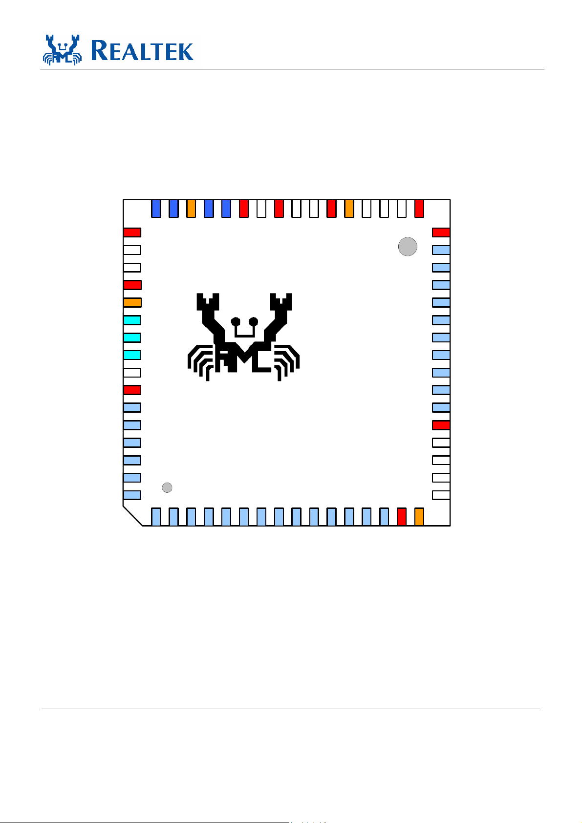
4. Pin Assignments
RTL8111B-GR
Datasheet
VDD15
NC
NC
VDD15
VDD33
LED3
LED2
LED1
LED0
VDD15
AVDD33
CKTAL1
CKTAL2
GVDD
EEDI/AUX
VDD33
EEDO
LLLLLLL TXXXV
EESK
48 47 46 45 44 43 42 41 40 39 38 37 36 35 34 33
49
50
51
52
53
54
55
56
57
58
59
60
61
62
EECS
VDD15
VDD15
NCNCNC
VDD15
RTL8111B
VDD33
ISOLATEB
NC
NC
VDD15
3
31
30
29
28
27
26
25
24
23
22
21
20
19
2
VDD15
EGND
HSON
HSOP
EVDD18
REFCLK_N
REFCLK_P
EGND
HSIN
HSIP
EVDD18
VDD15
PERSTB
LANW AKEB
VCTRL15
RSET
63
64
123456789
MDIP0
AVDD33
VCTRL18
MDIN0
MDIP1
AVDD18
Figure 1. Pin Assignments
MDIN1
10 11 12 13 14 15 16
AVDD18
MDIP2
MDIN2
MDIP3
AVDD18
18
7
1
VDD33
AVDD18
VDD15
MDIN3
NC
NC
4.1. Package Identification
‘Green’ package is indicated by a ‘G’ in the location marked ‘T’ in Figure 1.
Integrated Gigabit Ethernet Controller for PCI Express 3 Track ID: JATR-1076-21 Rev. 1.4
Page 9
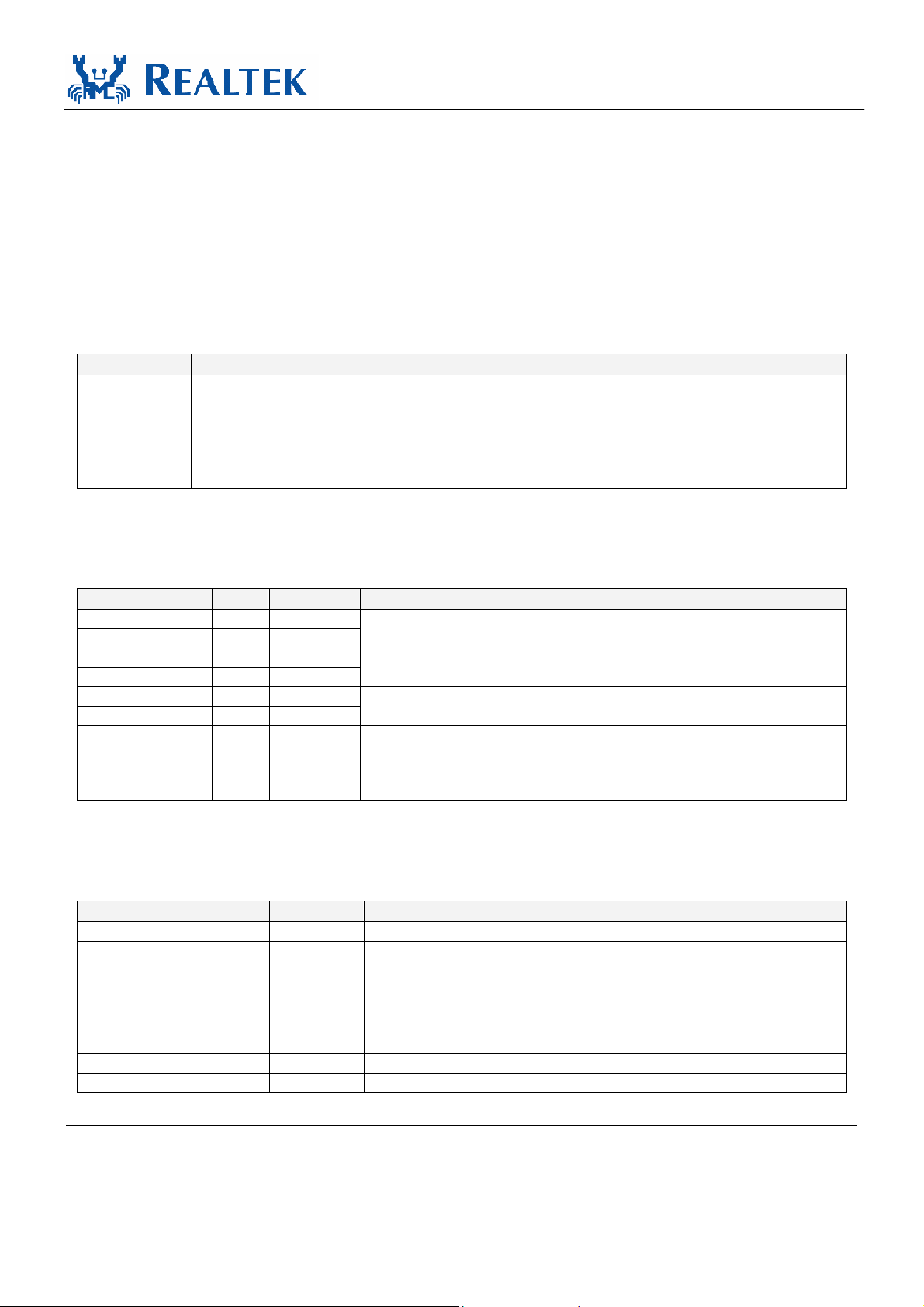
5. Pin Descriptions
The signal type codes below are used in the following tables:
I: Input S/T/S: Sustained Tri-State
O: Output O/D: Open Drain
T/S: Tri-State bi-directional input/output pin
5.1. Power Management/Isolation
Table 1. Power Management/Isolation
Symbol Type Pin No Description
LANWAKEB O/D 19
ISOLATEB I 36
Power Management Event: Open drain, active low.
Used to reactivate the PCI Express slot’s main power rails and reference clocks.
Isolate Pin: Active low.
Used to isolate the RTL8111B-GR from the PCI Express bus. The RTL8111B-GR
will not drive its PCI Express outputs (excluding LANWAKEB) and will not
sample its PCI Express input as long as the Isolate pin is asserted.
RTL8111B-GR
Datasheet
5.2. PCI Express Interface
Table 2. PCI Express Interface
Symbol Type Pin No Description
REFCLK_P I 26
REFCLK_N I 27
HSOP O 29
HSON O 30
HSIP I 23
HSIN I 24
PERSTB I 20
PCI Express Differential Reference Clock Source: 100MHz ± 300ppm.
PCI Express Transmit Differential Pair.
PCI Express Receive Differential Pair.
PCI Express Reset Signal: Active low.
When the PERSTB is asserted at power-on state, the RTL8111B-GR returns
to a pre-defined reset state and is ready for initialization and configuration
after the de-assertion of the PERSTB.
5.3. EEPROM
Table 3. EEPROM
Symbol Type Pin No Description
EESK O 48 Serial data clock.
EEDI: Output to serial data input pin of EEPROM.
AUX: Input pin to detect if Aux. Power exists or not on initial power-on.
EEDI/AUX O/I 47
EEDO I 45 Input from serial data output pin of EEPROM.
EECS O 44 EECS: EEPROM chip select.
This pin should be connected to EEPROM. To support wakeup from ACPI
D3cold or APM power-down, this pin must be pulled high to Aux. Power
via a resistor. If this pin is not pulled high to Aux. Power, the
RTL8111B-GR assumes that no Aux. Power exists.
Integrated Gigabit Ethernet Controller for PCI Express 4 Track ID: JATR-1076-21 Rev. 1.4
Page 10
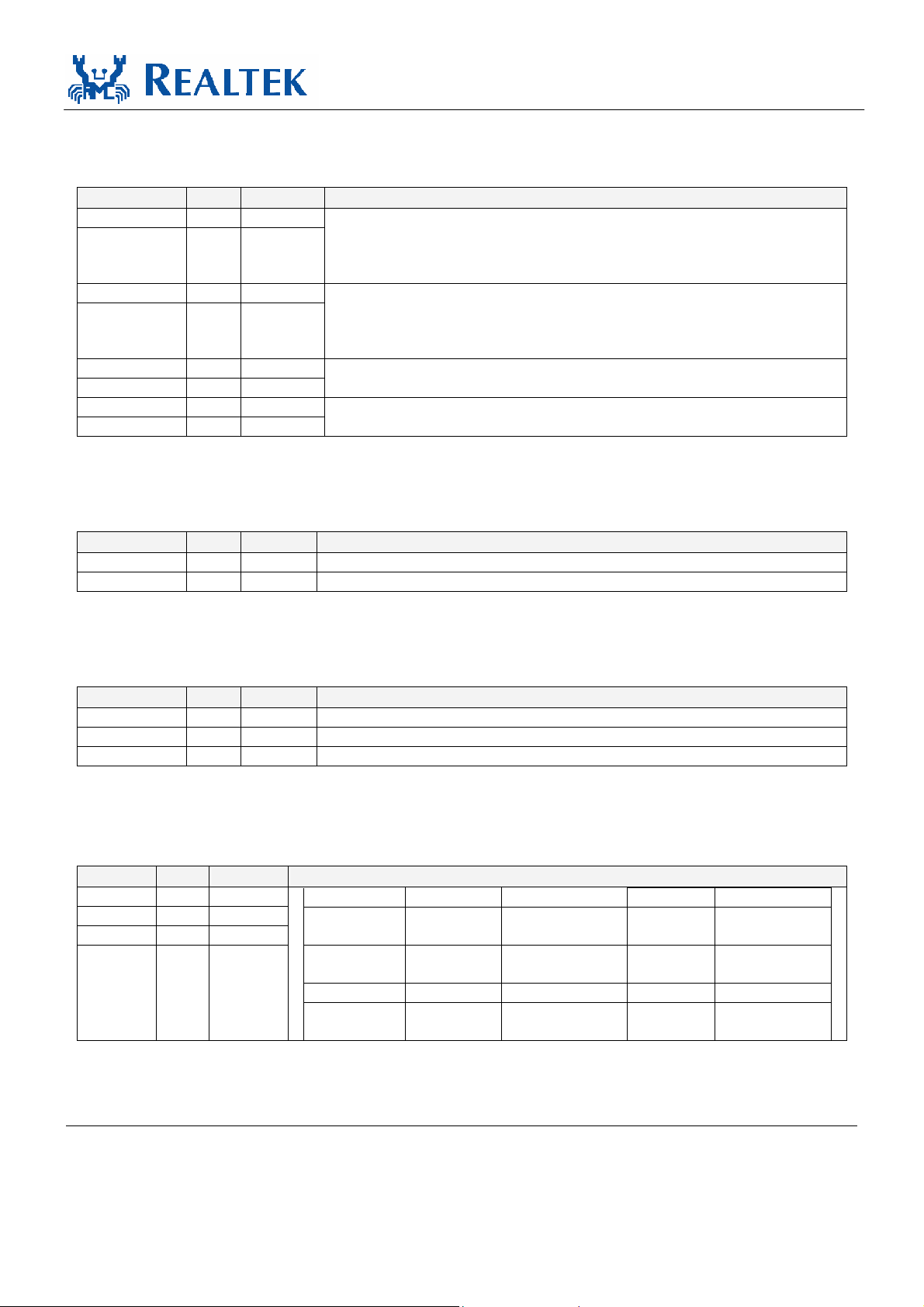
5.4. Transceiver Interface
Table 4. Transceiver Interface
Symbol Type Pin No Description
MDIP0 I/O 3
4
MDIN0 I/O
MDIP1 I/O 6
7
MDIN1 I/O
MDIP2 I/O 9
MDIN2 I/O 10
MDIP3 I/O 12
MDIN3 I/O 13
In MDI mode, this is the first pair in 1000Base-T, i.e. the BI_DA+/- pair, and is
the transmit pair in 10Base-T and 100Base-TX.
In MDI crossover mode, this pair acts as the BI_DB+/- pair, and is the receive
pair in 10Base-T and 100Base-TX.
In MDI mode, this is the second pair in 1000Base-T, i.e. the BI_DB+/- pair, and
is the transmit pair in 10Base-T and 100Base-TX.
In MDI crossover mode, this pair acts as the BI_DA+/- pair, and is the transmit
pair in 10Base-T and 100Base-TX.
In MDI mode, this is the third pair in 1000Base-T, i.e. the BI_DC+/- pair.
In MDI crossover mode, this pair acts as the BI_DD+/- pair.
In MDI mode, this is the fourth pair in 1000Base-T, i.e. the BI_DD+/- pair.
In MDI crossover mode, this pair acts as the BI_DC+/- pair.
5.5. Clock
RTL8111B-GR
Datasheet
Table 5. Clock
Symbol Type Pin No Description
CKTAL1 I 60 Input of 25MHz clock reference.
CKTAL2 O 61 Output of 25MHz clock reference.
5.6. Regulator & Reference
Table 6. Regulator & Reference
Symbol Type Pin No Description
VCTRL15 O 63 Regulator Control. Voltage control to external 1.5V power transistor.
VCTRL18 O 1 Regulator Control. Voltage control to external 1.8V power transistor.
RSET I 64 Reference. External resistor reference.
5.7. LEDs
Table 7. LEDs
Symbol Type Pin No Description
LED0 O 57
LED1 O 56
LED2 O 55
LED3 O 54
Note 1: During power down mode, the LED signals are logic high.
Note 2: LEDS1-0’s initial value comes from the 93C46. If there is no 93C46, the
default value of the (LEDS1, LEDS0) = (1, 1).
LEDS1-0 00 01 10 11
LED0 Tx/Rx
LED1 LINK100
LED2 LINK10 FULL Rx FULL
LED3 LINK1000 LINK1000 FULL
LINK10/1000/
ACT
LINK100/1000/
ACT
Tx LINK10/ACT
LINK
LINK100/
ACT
LINK1000/
ACT
Integrated Gigabit Ethernet Controller for PCI Express 5 Track ID: JATR-1076-21 Rev. 1.4
Page 11
RTL8111B-GR
Datasheet
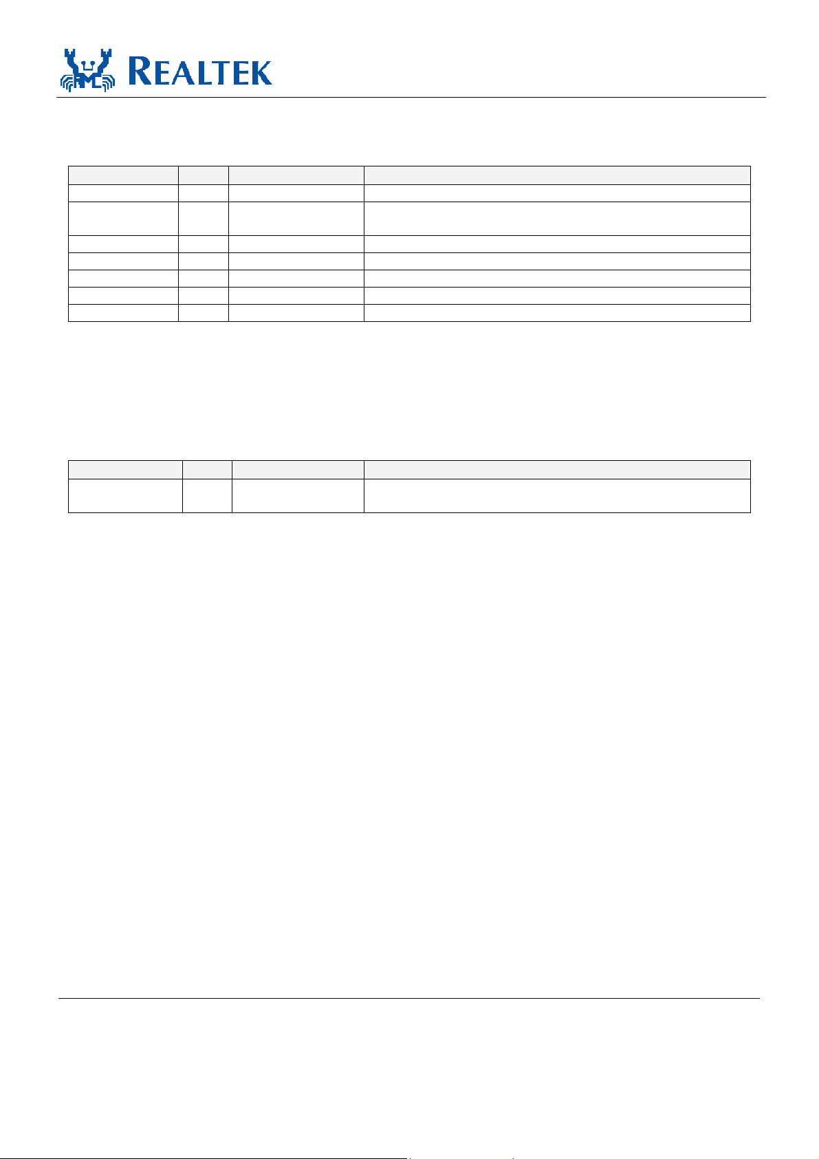
5.8. Power & Ground
Table 8. Power & Ground
Symbol Type Pin No Description
VDD33 Power 16, 37, 46, 53 Digital 3.3V power supply.
VDD15 Power
AVDD18 Power 5, 8, 11, 14 Analog 1.8V power supply.
EVDD18 Power 22, 28 Analog 1.8V power supply.
GVDD O 62 Output 1.5V.
AVDD33 Power 2, 59 Analog 3.3V power supply.
EGND Power 25, 31 Analog Ground.
Note 1: GVDD is tied to the internal 1.5V power supply. Do not connect this pin to any other power supply. Connect only
to two capacitors.
Note 2: Refer to the most updated schematic circuit for correct configuration.
15, 21, 32, 33, 38, 41,
43, 49, 52, 58
Digital 1.5V power supply.
5.9. NC (Not Connected) Pins
Table 9. NC (Not Connected) Pins
Symbol Type Pin No Description
NC
17, 18, 34, 35, 39, 40,
42, 50, 51
Not Connected.
Integrated Gigabit Ethernet Controller for PCI Express 6 Track ID: JATR-1076-21 Rev. 1.4
Page 12

RTL8111B-GR
Datasheet
6. Functional Description
6.1. PCI Express Bus Interface
The RTL8111B-GR is compliant with PCI Express Base Specification Revision 1.0a, and runs at a
2.5GHz signaling rate with X1 link width, i.e., one transmit and one receive differential pair. The
RTL8111B-GR supports four types of PCI Express messages: interrupt messages, error messages, power
management messages, and hot-plug messages. To ease PCB layout constraints, PCI Express lane
polarity reversal and link reversal are also supported.
6.1.1. PCI Express Transmitter
The RTL8111B-GR’s PCI Express block receives digital data from the Ethernet interface and performs
data scrambling with Linear Feedback Shift Register (LFSR) and 8B/10B coding technology into 10-bit
code groups. Data scrambling is used to reduce the possibility of electrical resonance on the link, and
8B/10B coding technology is used to benefit embedded clocking, error detection, and DC balance by
adding an overhead to the system through the addition of 2 extra bits. The data code groups are passed
through its serializer for packet framing. The generated 2.5Gbps serial data is transmitted onto the PCB
trace to its upstream device via a differential driver.
6.1.2. PCI Express Receiver
The RTL8111B-GR’s PCI Express block receives 2.5Gbps serial data from its upstream device to
generate parallel data. The receiver’s PLL circuits are re-synchronized to maintain bit and symbol lock.
Through 8B/10B decoding technology and data de-scrambling, the original digital data is recovered and
passed to the RTL8111B-GR’s internal Ethernet MAC to be transmitted onto the Ethernet media.
6.2. LED Functions
The RTL8111B-GR supports four LED signals in four different configurable operation modes. The
following sections describe the various LED actions.
6.2.1. Link Monitor
The Link Monitor senses link integrity, such as LINK10, LINK100, LINK1000, LINK10/100/1000,
LINK10/ACT, LINK100/ACT, or LINK1000/ACT. Whenever link status is established, the specific link
LED pin is driven low. Once a cable is disconnected, the link LED pin is driven high, indicating that no
network connection exists.
Integrated Gigabit Ethernet Controller for PCI Express 7 Track ID: JATR-1076-21 Rev. 1.4
Page 13
RTL8111B-GR
Datasheet
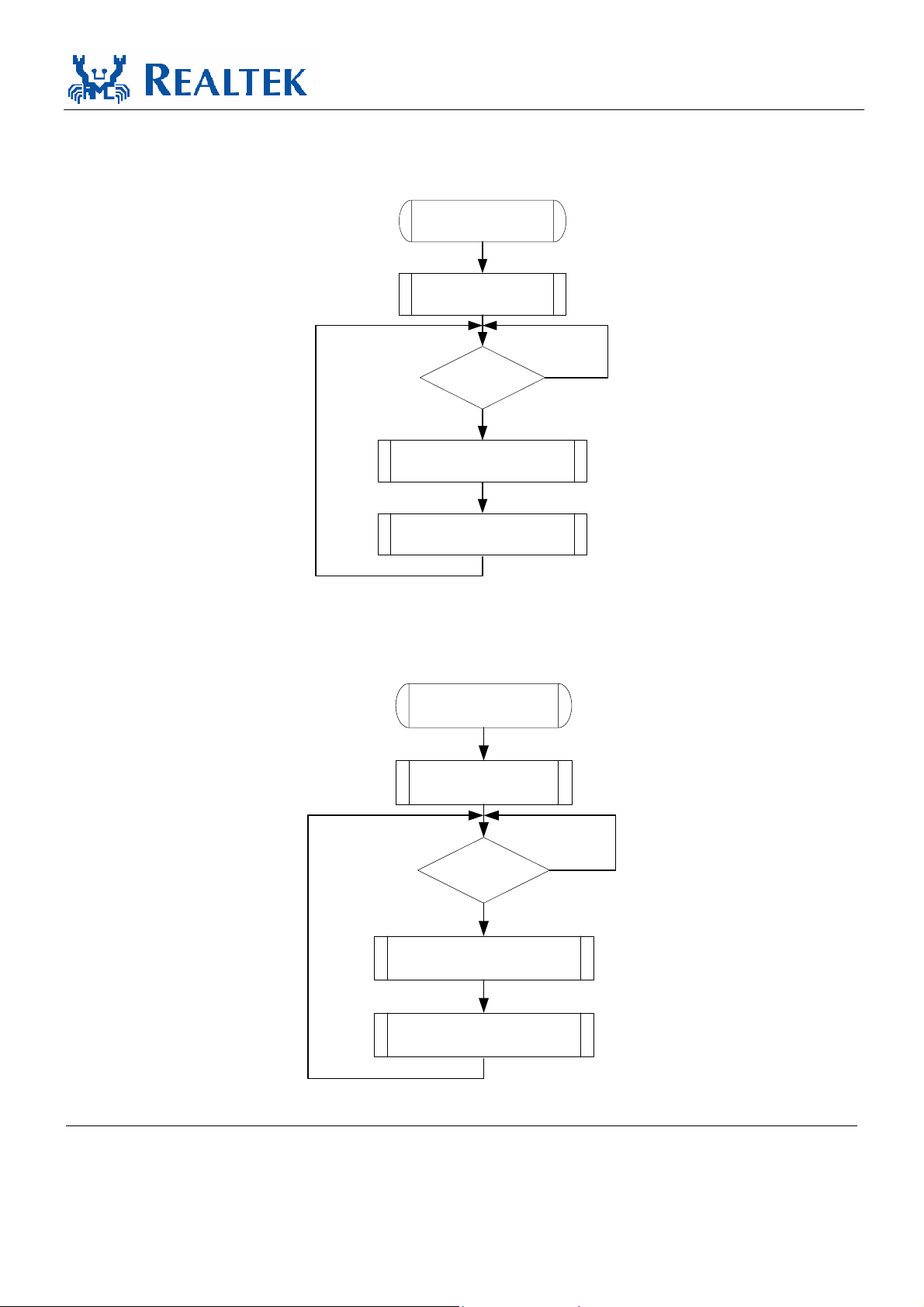
6.2.2. Rx LED
In 10/100/1000Mbps mode, blinking of the Rx LED indicates that receive activity is occurring.
Power On
LED = High
Receiving
Packet?
Yes
LED = High for 40 ms
LED = Low for 40 ms
No
Figure 2. Rx LED
6.2.3. Tx LED
In 10/100/1000Mbps mode, blinking of the Tx LED indicates that transmit activity is occurring.
Power On
LED = High
Transmitting
Packet?
Yes
LED = High for 40 ms
LED = Low for 40 ms
No
Figure 3. Tx LED
Integrated Gigabit Ethernet Controller for PCI Express 8 Track ID: JATR-1076-21 Rev. 1.4
Page 14
RTL8111B-GR
Datasheet
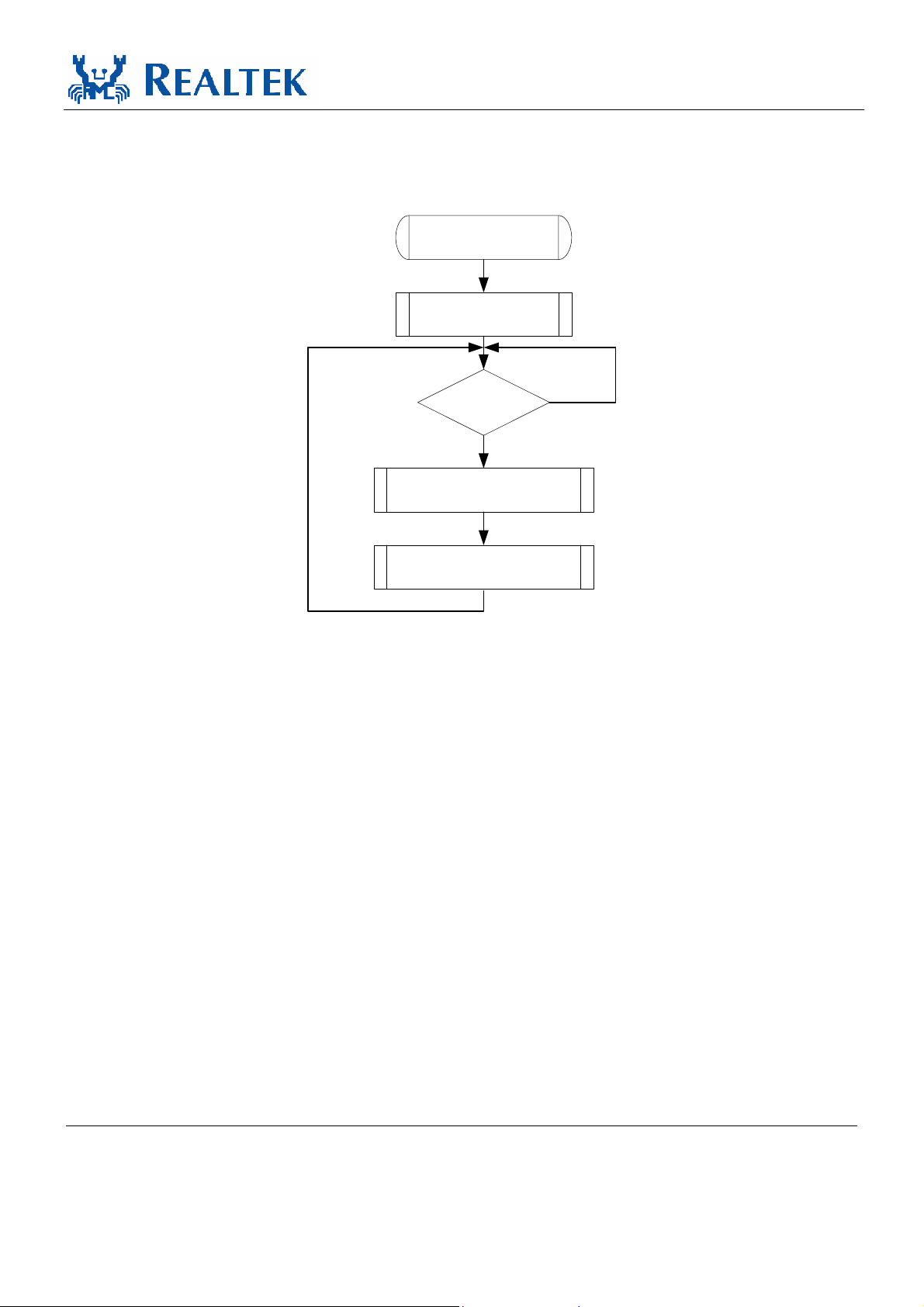
6.2.4. Tx/Rx LED
In 10/100/1000Mbps mode, blinking of the Tx/Rx LED indicates that both transmit and receive activity is
occurring.
Power On
LED = High
Tx/Rx Packet?
Yes
LED = High for 40 ms
LED = Low for 40 ms
Figure 4. Tx/Rx LED
No
Integrated Gigabit Ethernet Controller for PCI Express 9 Track ID: JATR-1076-21 Rev. 1.4
Page 15
RTL8111B-GR
Datasheet
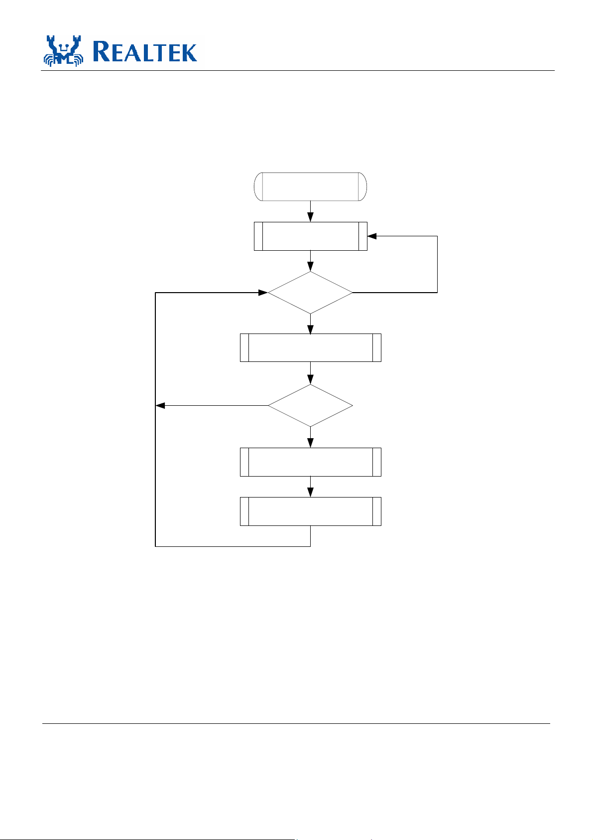
6.2.5. LINK/ACT LED
In 10/100/1000Mbps mode, blinking of the LINK/ACT LED indicates that the RTL8111B-GR is linked
and operating properly. When this LED is high for extended periods, it indicates that a link problem
exists.
Power On
LED = High
Link?
Yes
LED = Low
No
Figure 5. LINK/ACT LED
Tx/Rx
Packet?
Yes
LED = High for 40 ms
LED = Low for 40 ms
No
Integrated Gigabit Ethernet Controller for PCI Express 10 Track ID: JATR-1076-21 Rev. 1.4
Page 16

RTL8111B-GR
Datasheet
6.3. PHY Transceiver
6.3.1. PHY Transmitter
Based on state-of-the-art DSP technology and mixed-mode signal processing technology, the
RTL8111B-GR operates at 10/100/1000Mbps over standard CAT.5 UTP cable (100/1000Mbps), and
CAT.3 UTP cable (10Mbps).
GMII (1000Mbps) Mode
The RTL8111B-GR’s PCS layer receives data bytes from the MAC through the GMII interface and
performs the generation of continuous code-groups through 4D-PAM5 coding technology. These code
groups are passed through a waveform-shaping filter to minimize EMI effect, and are transmitted onto the
4-pair CAT5 cable at 125MBaud/s through a D/A converter.
MII (100Mbps) Mode
The transmitted 4-bit nibbles (TXD[3:0]) from the MAC, clocked at 25MHz (TXC), are converted into
5B symbol code through 4B/5B coding technology, then through scrambling and serializing, are
converted to 125Mhz NRZ and NRZI signals. After that, the NRZI signals are passed to the MLT3
encoder, then to the D/A converter and transmitted onto the media.
MII (10Mbps) Mode
The transmitted 4-bit nibbles (TXD[3:0]) from the MAC, clocked at 2.5MHz (TXC), are serialized into
10Mbps serial data. The 10Mbps serial data is converted into a Manchester-encoded data stream and is
transmitted onto the media by the D/A converter.
6.3.2. PHY Receiver
GMII (1000Mbps) Mode
Input signals from the media pass through the sophisticated on-chip hybrid circuit to subtract the
transmitted signal from the input signal for effective reduction of near-end echo. Afterwards, the received
signal is processed with state-of-the-art technology, e.g., adaptive equalization, BLW (Baseline Wander)
correction, cross-talk cancellation, echo cancellation, timing recovery, error correction, and 4D-PAM5
decoding. Then, the 8-bit-wide data is recovered and is sent to the GMII interface at a clock speed of
125MHz. The Rx MAC retrieves the packet data from the receive MII/GMII interface and sends it to the
Rx Buffer Manager.
MII (100Mbps) Mode
The MLT3 signal is processed with an ADC, equalizer, BLW (Baseline Wander) correction, timing
recovery, MLT3 and NRZI decoder, descrambler, 4B/5B decoder, and is then presented to the MII
interface in 4-bit-wide nibbles at a clock speed of 25MHz.
MII (10Mbps) Mode
The received differential signal is converted into a Manchester-encoded stream first. Next, the stream is
processed with a Manchester decoder and is de-serialized into 4-bit-wide nibbles. The 4-bit nibbles are
presented to the MII interface at a clock speed of 2.5MHz.
Integrated Gigabit Ethernet Controller for PCI Express 11 Track ID: JATR-1076-21 Rev. 1.4
Page 17

RTL8111B-GR
Datasheet
6.4. Next Page
If 1000Base-T mode is advertised, three additional Next Pages are automatically exchanged between the
two link partners. Users can set PHY Reg4.15 to 1 to manually exchange extra Next Pages via Reg7 and
Reg8 as defined in IEEE 802.3ab.
6.5. EEPROM Interface
The RTL8111B-GR requires the attachment of an external EEPROM. The 93C46/93C56 is a
1K-bit/2K-bit EEPROM. The EEPROM interface permits the RTL8111B-GR to read from, and write
data to, an external serial EEPROM device.
Values in the external EEPROM allow default fields in PCI configuration space and I/O space to be
overridden following a power-on or software EEPROM auto-load command. The RTL8111B-GR will
auto-load values from the EEPROM. If the EEPROM is not present, the RTL8111B-GR initialization
uses default values for the appropriate Configuration and Operational Registers. Software can read and
write to the EEPROM using bit-bang accesses via the 9346CR Register, or using PCI VPD (Vital Product
Data). The interface consists of EESK, EECS, EEDO, and EEDI.
The correct EEPROM (i.e. 93C46/93C56) must be used in order to ensure proper LAN function.
Table 10. EEPROM Interface
EEPROM Description
EECS 93C46/93C56 chip select.
EESK EEPROM serial data clock.
Input data bus/Input pin to detect whether Aux. Power exists on initial power-on.
EEDI/Aux
EEDO Output data bus.
This pin should be connected to EEPROM. To support wakeup from ACPI D3cold or
APM power-down, this pin must be pulled high to Aux. Power via a resistor. If this pin is
not pulled high to Aux. Power, the RTL8111B-GR assumes that no Aux. Power exists.
Integrated Gigabit Ethernet Controller for PCI Express 12 Track ID: JATR-1076-21 Rev. 1.4
Page 18

RTL8111B-GR
Datasheet
6.6. Power Management
The RTL8111B-GR is compliant with ACPI (Rev 1.0, 1.0b, 2.0), PCI Power Management (Rev 1.1), PCI
Express Active State Power Management (ASPM), and Network Device Class Power Management
Reference Specification (V1.0a), such as to support an Operating System-directed Power Management
(OSPM) environment.
The RTL8111B-GR can monitor the network for a Wakeup Frame, a Magic Packet, or a Re-LinkOk, and
notify the system via a PCI Express Power Management Event (PME) Message, Beacon, or
LANWAKEB pin when such a packet or event occurs. Then the system can be restored to a normal state
to process incoming jobs.
When the RTL8111B-GR is in power down mode (D1 ~ D3):
• The Rx state machine is stopped. The RTL8111B-GR monitors the network for wakeup events such as
a Magic Packet, Wakeup Frame, and/or Re-LinkOk, in order to wake up the system. When in power
down mode, the RTL8111B-GR will not reflect the status of any incoming packets in the ISR register
and will not receive any packets into the Rx on-chip buffer.
• The on-chip buffer status and packets that have already been received into the Rx on-chip buffer
before entering power down mode are held by the RTL8111B-GR.
• Transmission is stopped. PCI Express transactions are stopped. The Tx on-chip buffer is held.
• After being restored to D0 state, the RTL8111B-GR transmits data that was not moved into the Tx
on-chip buffer during power down mode. Packets that were not transmitted completely last time are
re-transmitted.
The D3cold_support_PME bit (bit15, PMC register) and the Aux_I_b2:0 bits (bit8:6, PMC register) in
PCI configuration space depend on the existence of Aux power (bit15, PMC) = 1.
If EEPROM D3cold_support_PME bit (bit15, PMC) = 0, the above 4 bits are all 0’s.
Example:
If EEPROM D3c_support_PME = 1:
• If aux. power exists, then PMC in PCI config space is the same as EEPROM PMC
(if EEPROM PMC = C2 F7, then PCI PMC = C2 F7)
• If aux. power is absent, then PMC in PCI config space is the same as EEPROM PMC except the
above 4 bits are all 0’s (if EEPROM PMC = C2 F7, then PCI PMC = 02 76)
In the above case, if wakeup support is desired when main power is off, it is suggested that the EEPROM
PMC be set to C2 F7 (Realtek EEPROM default value).
If EEPROM D3c_support_PME = 0:
• If aux. power exists, then PMC in PCI config space is the same as EEPROM PMC
(if EEPROM PMC = C2 77, then PCI PMC = C2 77)
• If aux. power is absent, then PMC in PCI config space is the same as EEPROM PMC except the
above 4 bits are all 0’s (if EEPROM PMC = C2 77, then PCI PMC = 02 76)
In the above case, if wakeup support is not desired when main power is off, it is suggested that the
EEPROM PMC be set to 02 76.
Integrated Gigabit Ethernet Controller for PCI Express 13 Track ID: JATR-1076-21 Rev. 1.4
Page 19

RTL8111B-GR
Datasheet
Link Wakeup occurs only when the following conditions are met:
• The LinkUp bit (CONFIG3#4) is set to 1, the PMEn bit (CONFIG1#0) is set to 1, and the
corresponding wake-up method (message, beacon, or LANWAKEB) can be asserted in the current
power state.
Magic Packet Wakeup occurs only when the following conditions are met:
• The destination address of the received Magic Packet is acceptable to the RTL8111B-GR, e.g., a
broadcast, multicast, or unicast packet addressed to the current RTL8111B-GR adapter.
• The received Magic Packet does not contain a CRC error.
• The Magic bit (CONFIG3#5) is set to 1, the PMEn bit (CONFIG1#0) is set to 1, and the
corresponding wake-up method (message, beacon, or LANWAKEB) can be asserted in the current
power state.
• The Magic Packet pattern matches, i.e. 6 * FFh + MISC (can be none) + 16 * DID (Destination ID) in
any part of a valid Ethernet packet.
A Wakeup Frame event occurs only when the following conditions are met:
• The destination address of the received Wakeup Frame is acceptable to the RTL8111B-GR, e.g., a
broadcast, multicast, or unicast address to the current RTL8111B-GR adapter.
• The received Wakeup Frame does not contain a CRC error.
• The PMEn bit (CONFIG1#0) is set to 1.
• The 16-bit CRCA of the received Wakeup Frame matches the 16-bit CRC of the sample Wakeup
Frame pattern given by the local machine’s OS. Or, the RTL8111B-GR is configured to allow direct
packet wakeup, e.g., a broadcast, multicast, or unicast network packet.
Note: 16-bit CRC: The RTL8111B-GR supports two normal wakeup frames (covering 64 mask bytes
from offset 0 to 63 of any incoming network packet) and three long wakeup frames (covering 128
mask bytes from offset 0 to 127 of any incoming network packet).
The corresponding wake-up method (message, beacon, or LANWAKEB) is asserted only when the
following conditions are met:
• The PMEn bit (bit0, CONFIG1) is set to 1.
• The PME_En bit (bit8, PMCSR) in PCI Configuration Space is set to 1.
• The RTL8111B-GR may assert the corresponding wake-up method (message, beacon, or
LANWAKEB) in the current power state or in isolation state, depending on the PME_Support
(bit15-11) setting of the PMC register in PCI Configuration Space.
• A Magic Packet, LinkUp, or Wakeup Frame has been received.
• Writing a 1 to the PME_Status (bit15) of the PMCSR register in the PCI Configuration Space clears
this bit and causes the RTL8111B-GR to stop asserting the corresponding wake-up method (message,
beacon, or LANWAKEB) (if enabled).
Integrated Gigabit Ethernet Controller for PCI Express 14 Track ID: JATR-1076-21 Rev. 1.4
Page 20

RTL8111B-GR
Datasheet
When the RTL8111B-GR is in power down mode, e.g., D1-D3, the IO and MEM accesses to the
RTL8111B-GR are disabled. After a PERSTB assertion, the device’s power state is restored to D0
automatically if the original power state was D3
power state transition. When in ACPI mode, the device does not support PME (Power Management
Enable) from D0 (this is the Realtek default setting of the PMC register auto-loaded from EEPROM). The
setting may be changed from the EEPROM, if required.
. There is almost no hardware delay at the device’s
cold
6.7. Vital Product Data (VPD)
Bit 31 of the Vital Product Data (VPD) capability structure in the RTL8111B-GR’s PCI Configuration
Space is used to issue VPD read/write commands and is also a flag used to indicate whether the transfer
of data between the VPD data register and the 93C46/93C56 has completed or not.
1. Write VPD register: (write data to the 93C46/93C56)
Set the flag bit to 1 at the same time the VPD address is written to write VPD data to EEPROM.
When the flag bit is reset to 0 by the RTL8111B-GR, the VPD data (4 bytes per VPD access)
has been transferred from the VPD data register to EEPROM.
2. Read VPD register: (read data from the 93C46/93C56)
Reset the flag bit to 0 at the same time the VPD address is written to retrieve VPD data from
EEPROM. When the flag bit is set to 1 by the RTL8111B-GR, the VPD data (4 bytes per VPD
access) has been transferred from EEPROM to the VPD data register.
Note1: Refer to the PCI 2.2 Specifications for further information.
Note2: The VPD address must be a DWORD-aligned address as defined in the PCI 2.2 Specifications.
VPD data is always consecutive 4-byte data starting from the VPD address specified.
Note3: Realtek reserves offset 40h to 7Fh in EEPROM mainly for VPD data to be stored.
Note4: The VPD function of the RTL8111B-GR is designed to be able to access the full range of the
93C46/93C56 EEPROM.
Integrated Gigabit Ethernet Controller for PCI Express 15 Track ID: JATR-1076-21 Rev. 1.4
Page 21
RTL8111B-GR
Datasheet
7. Characteristics
7.1. Absolute Maximum Ratings
WARNING: Absolute maximum ratings are limits beyond which permanent damage may be caused to
the device, or device reliability will be affected. All voltages are specified reference to GND unless
otherwise specified.
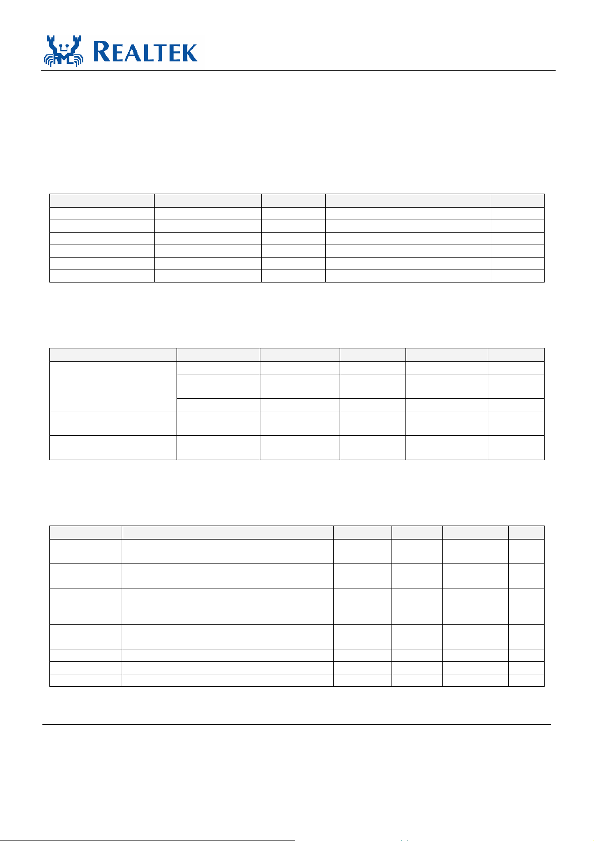
Table 11. Absolute Maximum Ratings
Symbol Description Minimum Maximum Unit
VDD33, AVDD33 Supply Voltage 3.3V -0.5 4.6 V
EVDD18,AVDD18 Supply Voltage 1.8V -0.5 2.1 V
VDD15 Supply Voltage 1.5V -0.5 2 V
DCinput Input Voltage -0.5 Corresponding Supply Voltage + 0.5 V
DCoutput Output Voltage -0.5 Corresponding Supply Voltage + 0.5 V
Storage Temperature -55 +125 °C
* Refer to the most updated schematic circuit for correct configuration.
7.2. Recommended Operating Conditions
Table 12. Recommended Operating Conditions
Description Pins Minimum Ty pical Maximum Unit
VDD33, AVDD33 3.0 3.3 3.6 V
Supply Voltage VDD
Ambient Operating
Temperature T
Maximum Junction
Temperature
* Refer to the most updated schematic circuit for correct configuration.
A
EVDD18,
AVDD18
VDD15 1.35 1.5 1.65 V
0 70 °C
125 °C
1.6 1.8 1.98 V
7.3. Crystal Requirements
Table 13. Crystal Requirements
Symbol Description/Condition Minimum Typical Maximum Unit
F
ref
F
Stability
ref
F
Tolerance
ref
F
ref
Duty Cycle
C
L
ESR Equivalent Series Resistance.
DL
Integrated Gigabit Ethernet Controller for PCI Express 16 Track ID: JATR-1076-21 Rev. 1.4
Parallel resonant crystal reference frequency,
fundamental mode, AT-cut type.
Parallel resonant crystal frequency stability,
fundamental mode, AT-cut type. T
Parallel resonant crystal frequency tolerance,
fundamental mode, AT-cut type.
T
=-20°C ~+70°C.
a
Reference clock input duty cycle. 40 60 %
Load Capacitance. pF
Drive Level. 0.5 mW
=25°C.
a
25 MHz
-50 +50 ppm
-30 +30 ppm
Page 22
RTL8111B-GR
Datasheet
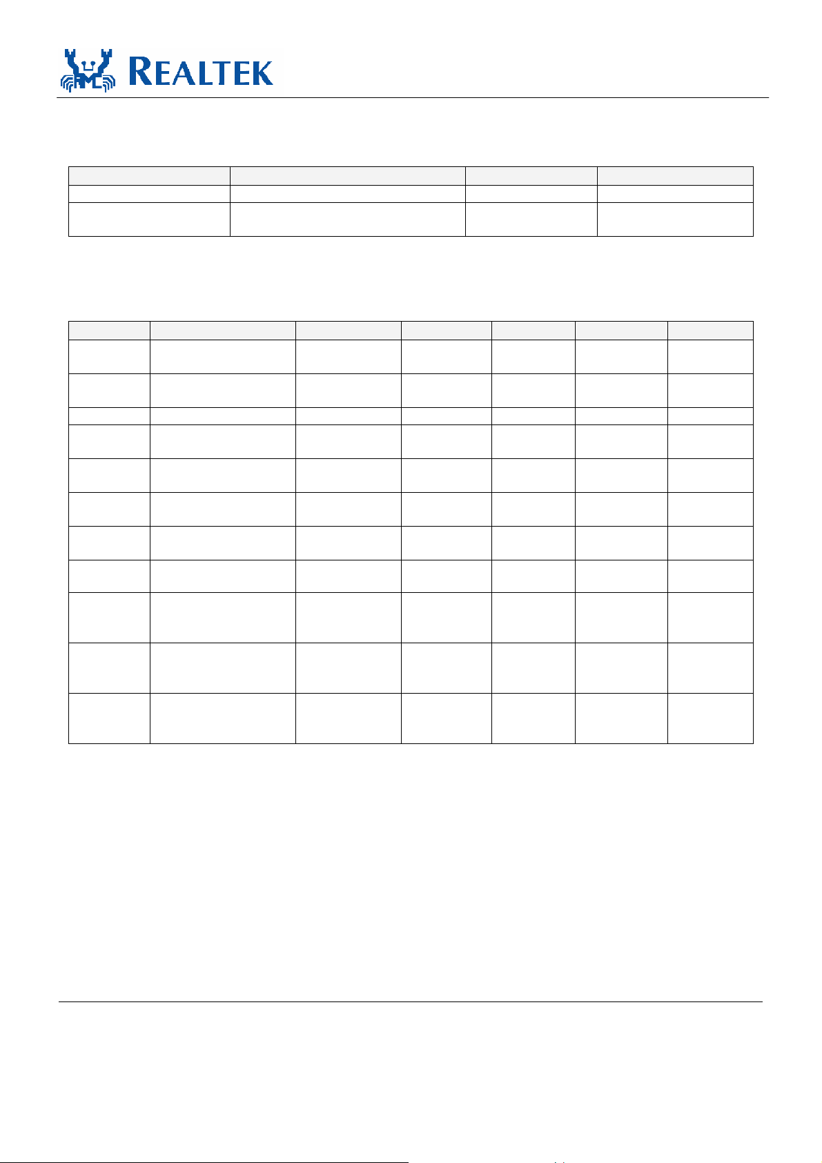
7.4. Thermal Characteristics
Table 14. Thermal Characteristics
Parameter Minimum Maximum Units
Storage Temperature -55 +125 °C
Ambient Operating
Temperature
0 70 °C
7.5. DC Characteristics
Table 15. DC Characteristics
Symbol Parameter Conditions Minimum Typi cal Maximum Units
VDD33,
AVDD33
EVDD18,
AVDD18
VDD15 1.5V Supply Voltage 1.35 1.5 1.65 V
Vo h
Vo l
Vih
Vil
Iin
Icc33
Icc18
Icc15
* Refer to the most updated schematic circuit for correct configuration.
3.3V Supply Voltage 3.0 3.3 3.6 V
1.8V Supply Voltage 1.6 1.8 1.98 V
Minimum High Level
Output Voltage
Maximum Low Level
Output Voltage
Minimum High Level
Input Voltage
Maximum Low Level
Input Voltage
Input Current
Average Operating
Supply Current from
3.3V
Average Operating
Supply Current from
1.8V
Average Operating
Supply Current from
1.5V
Ioh
= -8mA
Iol= 8mA
Vin = VDD33 or
GND
At 1Gbps with
heavy network
traffic
At 1Gbps with
heavy network
traffic
At 1Gbps with
heavy network
traffic
0.9 * VDD33 VDD33 V
0.1 * VDD33 V
0.5 * VDD33 VDD33+0.5 V
-0.5 0.3 * VDD33 V
-1.0 1.0 µA
103 mA
198 mA
367 mA
Integrated Gigabit Ethernet Controller for PCI Express 17 Track ID: JATR-1076-21 Rev. 1.4
Page 23
7.6. AC Characteristics
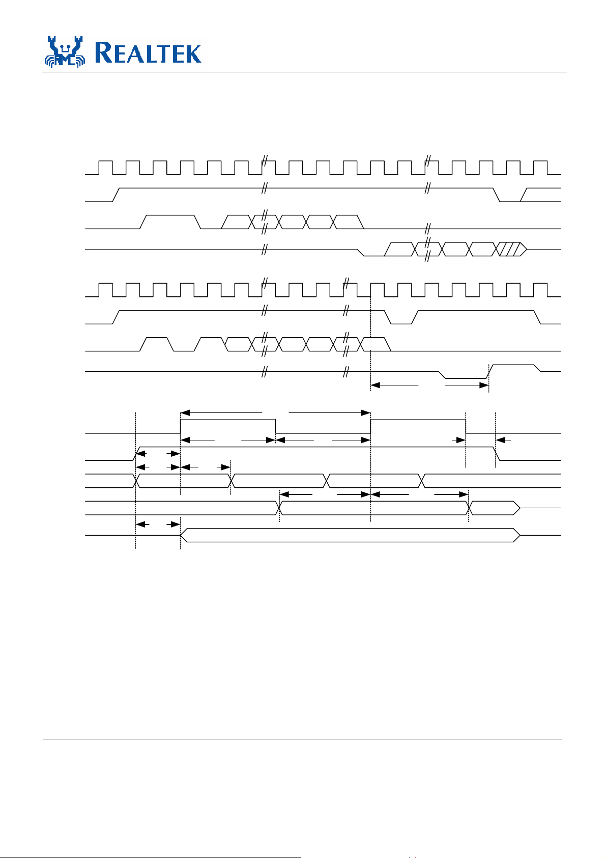
7.6.1. Serial EEPROM Interface Timing
93C46(64*16)/93C56(128*16)
EESK
RTL8111B-GR
Datasheet
EECS
EEDI
EEDO
EESK
EECS
EEDI
EEDO
EESK
EECS
EEDI
EEDO
EEDO
(Read)
(Read)
High Impedance
(Write)
(Write)
High Impedance
(Read)
(Program)
11
0
110
tcss
tdis tdih
tsv
Figure 6. Serial EEPROM Interface Timing
An A2 A0A1
...
An A0
tsk
tskh tskl
Dn
tdos tdoh
0
...
D0
STATUS VALID
tcs
Dn D1 D0
tcs
BUSY READY
twp
tcsh
Integrated Gigabit Ethernet Controller for PCI Express 18 Track ID: JATR-1076-21 Rev. 1.4
Page 24

RTL8111B-GR
Table 16. EEPROM Access Timing Parameters
Symbol Parameter EEPROM Type Min. Max. Unit
tcs Minimum CS Low Time 9346 1000 ns
twp Write Cycle Time 9346 10 ms
tsk SK Clock Cycle Time 9346 4 µs
tskh SK High Time 9346 1000 ns
tskl SK Low Time 9346 1000 ns
tcss CS Setup Time 9346 200 ns
tcsh CS Hold Time 9346 0 ns
tdis DI Setup Time 9346 400 ns
tdih DI Hold Time 9346 400 ns
tdos DO Setup Time 9346 2000 ns
tdoh DO Hold Time 9346 2000 ns
tsv CS to Status Valid 9346 1000 ns
Datasheet
Integrated Gigabit Ethernet Controller for PCI Express 19 Track ID: JATR-1076-21 Rev. 1.4
Page 25

RTL8111B-GR
Datasheet
7.7. PCI Express Bus Parameters
7.7.1. Differential Transmitter Parameters
Table 17. Differential Transmitter Parameters
Symbol Parameter Min Typical Max Units
UI
V
TX-DIFFp-p
V
TX-DE-RATIO
T
TX-EYE
T
TX-EYE-MEDIAN-
to-MAX-JITTER
T
V
V
IDLEDELTA
V
DELTA
V
V
, T
TX-RISE
TX-CM-ACp
TX-CM-DCACTIVE-
TX-FALL
TX-CM-DCLINE-
TX-IDLE-DIFFp
TX-RCV-DETECT
Electrical Idle Differential Peak Output Voltage 0 20 mV
Unit Interval
Differential Peak to Peak Output Voltage 0.800 1.2 V
De-Emphasized Differential Output Voltage (Ratio) -3.0 -3.5 -4.0 dB
Minimum Tx Eye Width 0.70 UI
Maximum time between the jitter median and
maximum deviation from the median
D+/D- Tx Output Rise/Fall Time 0.125 UI
RMS AC Peak Common Mode Output Voltage 20 mV
Absolute Delta of DC Common Mode Voltage During
L0 and Electrical Idle
Absolute Delta of DC Common Mode Voltage between
D+ and D-
The amount of voltage change allowed during
Receiver Detection
V
TX-DC-CM
I
TX-SHORT
T
TX-IDLE-MIN
T
TX-IDLE- SETTO-IDLE
The TX DC Common Mode Voltage 0 3.6 V
TX Short Circuit Current Limit 90 mA
Minimum time spent in Electrical Idle 50 UI
Maximum time to transition to a valid Electrical Idle
after sending an Electrical Idle ordered set
T
TX-IDLE-TOTO-
DIFF-DATA
RL
RL
Z
Z
L
Differential Return Loss 12 dB
TX-DIFF
Common Mode Return Loss 6 dB
TX-CM
TX-DIFF-DC
TX-DC
TX-SKEW
DC Differential TX Impedance 80 100 120
Transmitter DC Impedance 40
Lane-to-Lane Output Skew 500+2
Maximum time to transition to valid TX specifications
after leaving an Electrical Idle condition
CTX AC Coupling Capacitor 75 200 nF
T
Crosslink Random Timeout 0 1 ms
crosslink
Note1: Refer to PCI Express Base Specification, rev.1.0a, for correct measurement environment setting of each
parameter.
Note2: The data rate can be modulated with an SSC (Spread Spectrum Clock) from +0 to -0.5% of the nominal data rate
frequency, at a modulation rate in the range not exceeding 30 kHz – 33 kHz. The +/- 300 ppm requirement still holds,
which requires the two communicating ports be modulated such that they never exceed a total of 600 ppm difference.
2
399.88 400 400.12 ps
0.15 UI
0 100 mV
0 25 mV
600 mV
20 UI
20 UI
ps
UI
Integrated Gigabit Ethernet Controller for PCI Express 20 Track ID: JATR-1076-21 Rev. 1.4
Page 26
RTL8111B-GR
Datasheet
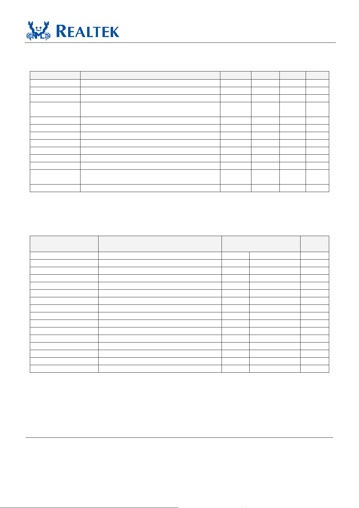
7.7.2. Differential Receiver Parameters
Table 18. Differential Receiver Parameters
Symbol Parameter Min. Typical Max. Units
UI Unit Interval 399.88 400 400.12 ps
V
RX-DIFFp-p
T
RX-EYE
T
RX-EYE-MEDIAN-to-
MAX-JITTER
V
RX-CM-ACp
RL
RL
Z
RX-DIFF-DC
Z
RX--DC
Z
RX-HIGH-IMP-DC
V
RX-IDLE-DET-DIFFp-p
T
RX-IDLE-DET-
DIFFENTERTIME
L
RX-SKEW
Differential Return Loss 15 dB
RX-DIFF
RX-CM
DC Differential Input Impedance 80 100 120
DC Input Impedance 40 50 60
Total Skew 20 ns
Note: Refer to PCI Express Base Specification, rev.1.0a, for correct measurement environment setting of each parameter.
Differential Input Peak to Peak Voltage 0.175 1.200 V
Minimum Receiver Eye Width 0.4 UI
Maximum time between the jitter median and
0.3 UI
maximum deviation from the median
AC Peak Common Mode Input Voltage 150 mV
Common Mode Return Loss 6 dB
Powered Down DC Input Impedance 200 k
Electrical Idle Detect Threshold 65 175 mV
Unexpected Electrical Idle Enter Detect Threshold
10 ms
Integration Time
7.7.3. REFCLK Parameters
Table 19. REFCLK Parameters
Symbol Parameter 100MHz Input
Min Max
T
Absolute min. DIF CLK Period 9.872 ns
absmin
T
rise
T
fall
h T
T
rise
fall
Rise Time 175 700 ps
Fall Time 175 700 ps
Rise Time Variation 125 ps
Fall Time Variation 125 ps
Rise/Fall Matching 20 %
V
high
V
Voltage Low (typical 0.0V) -150 mV
low
V
cross absolute
V
cross relative
Total V
T
ccjitter
Absolute Crossing Point Voltages 250 550 mV
Relative Crossing Point Voltages Note
Total Variation of V
cross
Cycle to Cycle Jitter 125 ps
Voltage High (typical 0.71V) 660 850 mV
2
over all edges 140 mV
cross
Note
2
Duty Cycle 45 55 %
V
Maximum Voltage (Overshoot) V
ovs
V
Minimum Voltage (Undershoot) -0.3 V
uds
+ 0.3 V
high_avg
Vrb Ringback Voltage 0.2 N/A V
Note1: Refer to PCI Express Base Specification, rev.1.0a, for correct measurement environment setting of each
parameter.
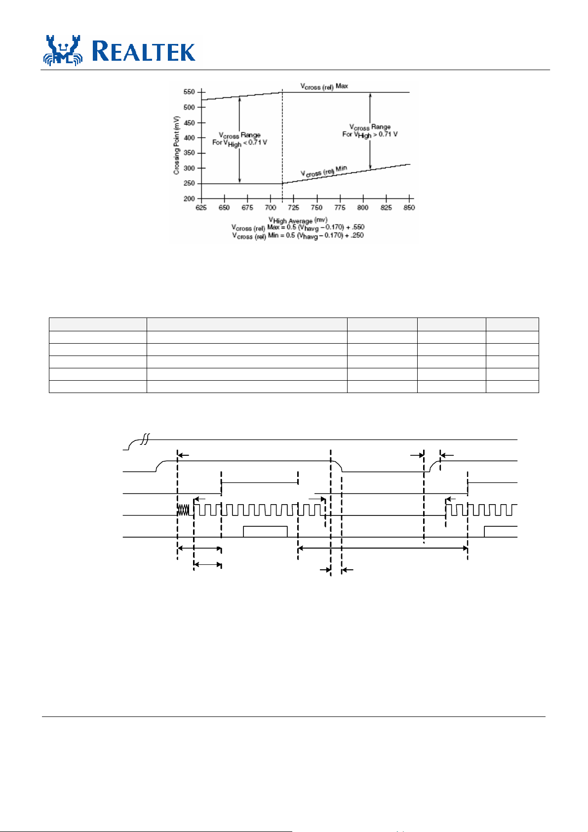
Note2: Vcross relative Min = 0.5(Vhigh_avg – 0.710) + 0.250, Vcross relative Max = 0.5(Vhigh_avg – 0.710) + 0.550.
The crossing point must meet the absolute and relative crossing point specifications simultaneously.
Note3: The nominal single-ended swing for each clock is 0 to 0.7V with a nominal frequency of 100MHz ±300 PPM.
Note4: The reference clocks may support spread spectrum clocking. The minimum clock period cannot be violated.
Units
V
Integrated Gigabit Ethernet Controller for PCI Express 21 Track ID: JATR-1076-21 Rev. 1.4
Page 27
RTL8111B-GR
Datasheet
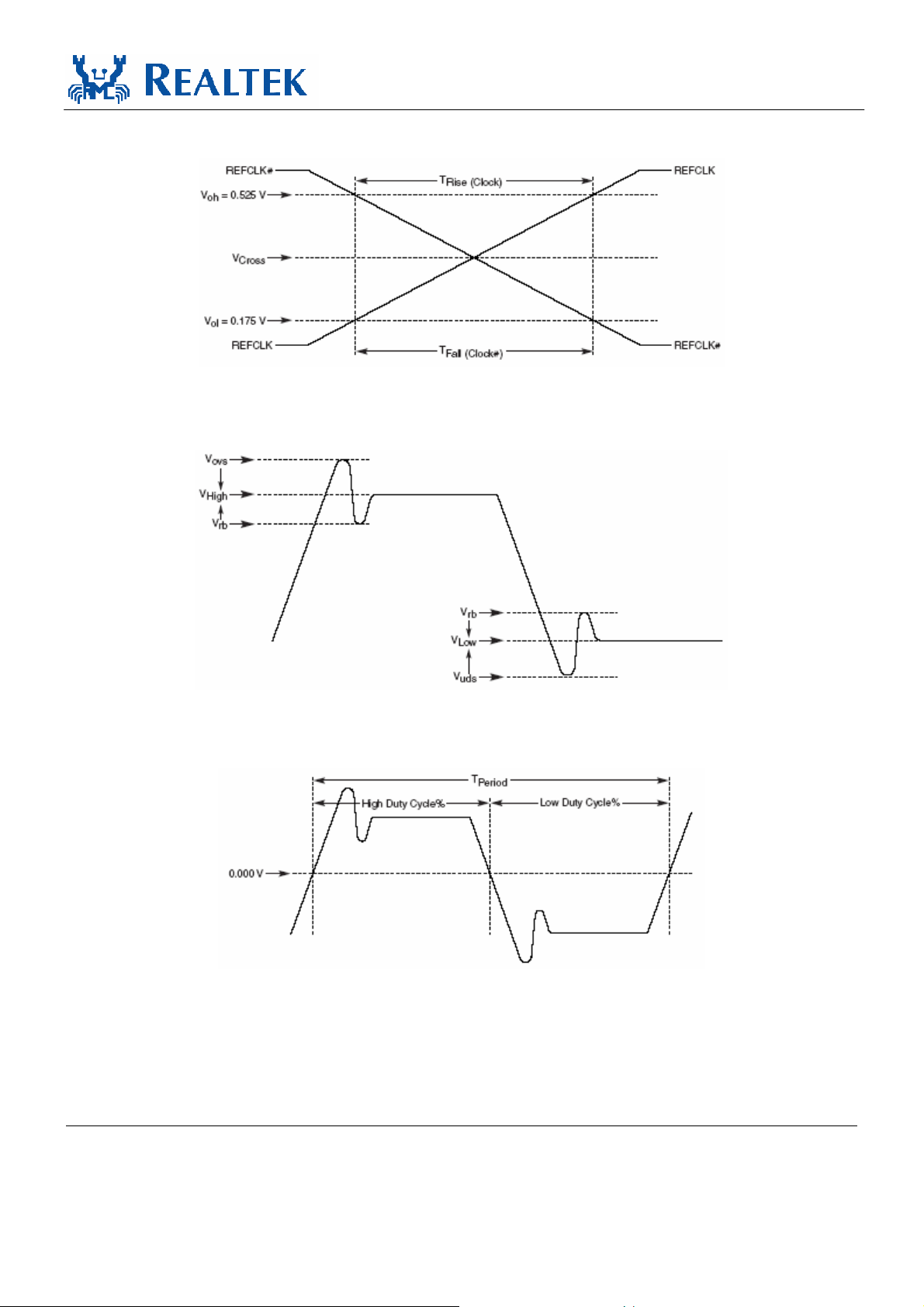
Figure 7. REFCLK Single-Ended Measurement Points for T
rise
and T
fall
Figure 8. REFCLK Single-Ended Measurement Points for V
ovs
, V
uds,
and V
rb
Figure 9. REFCLK Differential Measurement Points for T
, Duty Cycle, and Jitter
period
Integrated Gigabit Ethernet Controller for PCI Express 22 Track ID: JATR-1076-21 Rev. 1.4
Page 28
RTL8111B-GR
Datasheet
Figure 10. REFCLK V
cross
Range
7.7.4. Auxiliary Signal Timing Parameters
Table 20. Auxiliary Signal Timing Parameters
Symbol Parameter Min Max Units
T
Power stable to PERSTB inactive 100 ms
PVPERL
T
PERST-CLK
T
PERST
T
FAI L
T
WKRF
REFCLK stable before PERSTB inactive 100 µs
PERSTB active time 100 µs
Power level invalid to PWRGD inactive 500 ns
LANWAKEB rise – fall time 100 ns
3.3 Vaux
Power Stable
Wakeup Event
Power Stable
3.3/12V
PERSTB
Clock Stable Clock Stable
Clock not
Stable
REFCLK
PCI-E Link
Inactive
T
PVPERL
T
PERST-CLK
Active
T
FAIL
Inactive
T
PERST
Active
Figure 11. Auxiliary Signal Timing
Integrated Gigabit Ethernet Controller for PCI Express 23 Track ID: JATR-1076-21 Rev. 1.4
Page 29
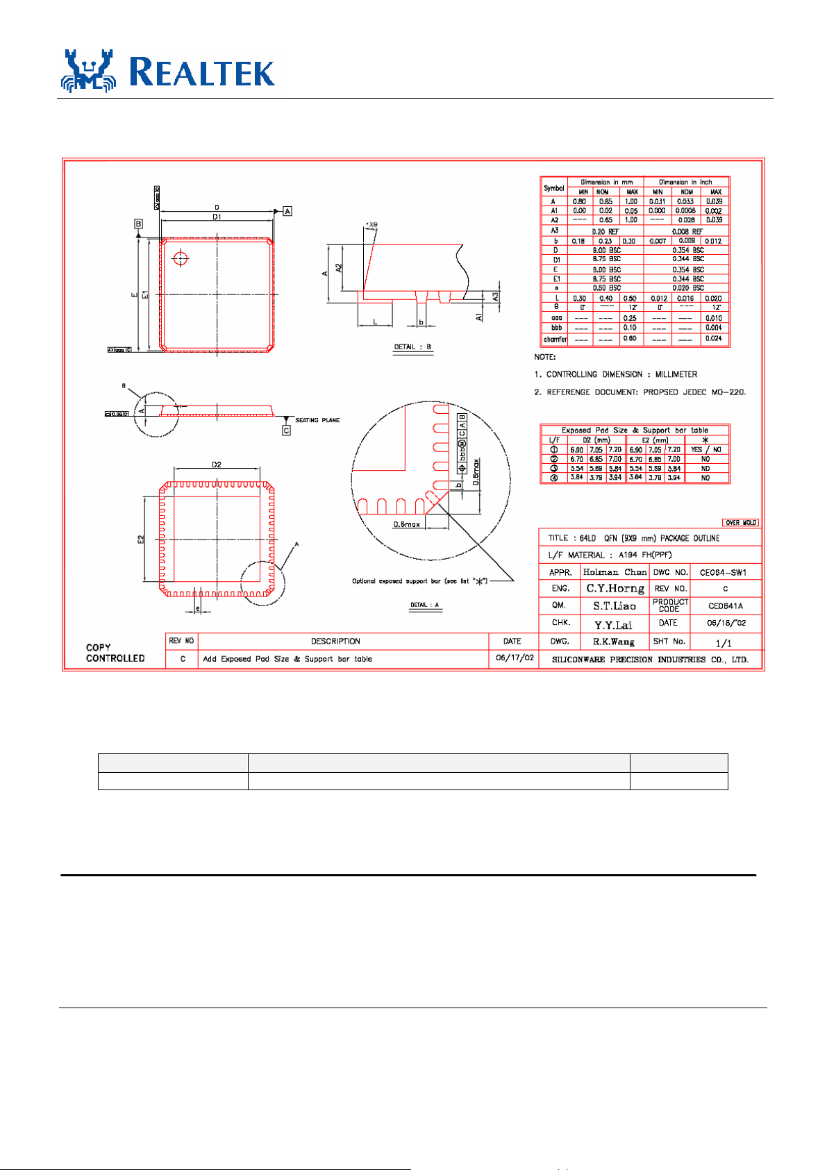
8. Mechanical Dimensions
RTL8111B-GR
Datasheet
9. Ordering Information
Table 21. Ordering Information
Part Number Package Status
RTL8111B-GR 64-Pin QFN ‘Green’ package
Note: See page 3 for package ID information.
Realtek Semiconductor Corp.
Headquarters
No. 2, Innovation Road II
Hsinchu Science Park, Hsinchu 300, Taiwan
Tel.: +886-3-578-0211. Fax: +886-3-577-6047
www.realtek.com.tw
NOTE: RTL8111B’s exposed pad size is L/F ○3
Integrated Gigabit Ethernet Controller for PCI Express 24 Track ID: JATR-1076-21 Rev. 1.4
 Loading...