

Page 1
Preliminary
RT9264
High Frequency, High Efficiency, Step-up DC/DC Converter
General Description
The RT9264 is a compact, high efficient, step-up
DC/DC converter with current mode PWM control
loop, providing stable and high efficient operations
without external compensation.
The RT9264 suitable for 1 to 4 battery cells as well
as USB power applications providing up to 400mA
output current. The high switching rate minimized
the size of external components.
A 300mA LDO is included in RT9264 to provide a
secondary low noise output as well as an output
current stop in the shutdown mode. RT9264 is
provided in SOP-8 packages.
Ordering Information
RT9264
Package type
S : SOP-8
Operating temperature range
C: Commercial standard
Features
z
400mA High Supply Capability
z
90% Efficiency
z
Switching Rate higher Than 1.4MHz
z
Providing Flexibility for Using Internal and
External Power Switches
z
Built-in 300mA LDO, also for the Zero-Output-
Current Shutdown Mode
z
Boost DC-DC Integrating LDO for Up-Down
Regulation
z
8-Pin SOP Package
Applications
Portable Instrument
z
ADSL Modem
z
USB Devices
z
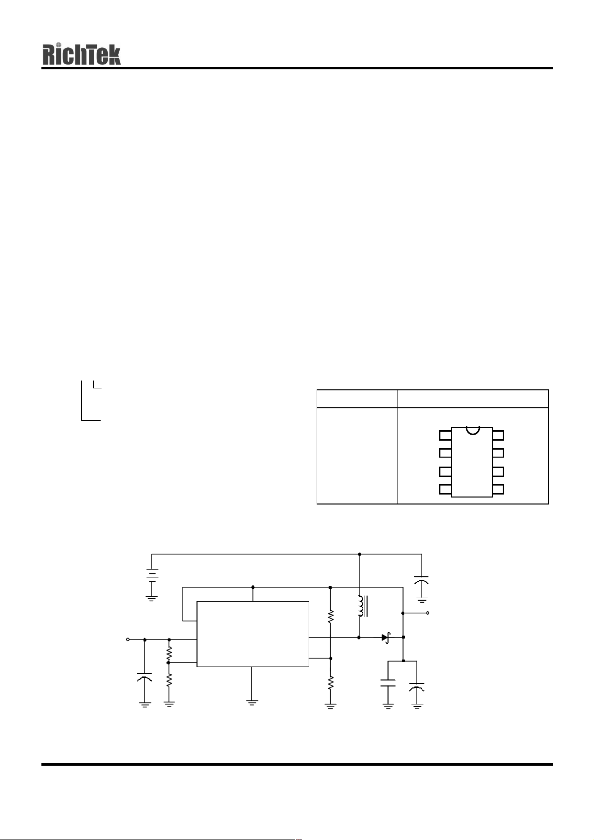
Pin Configurations
Part Number Pin Configurations
EXT
TOP VIEW
1
2
CE
8
LX
7
RT9264CS
(Plastic SOP-8)
GND
Typical Application Circuit
V
IN
CE
V
2.5V
OU T2
+
C3
10µF
Fig. 1 RT9264 Typical Application for Portable Instruments
LDOO LX
R4
42K
LFB GND FB
R3
22K
VDD
RT9264
EXT
R1
36K
R2
22K
L1
2.2µH
D1
1N5819
C2
1µF
LFB
LDOO
+
C1
47µF
3
4
47µF
3.3V
V
OU T1
6
VDD
5
FB
DS9264-00 December 2001 www.richtek-ic.com.tw
1
Page 2

RT9264
Preliminary
V
IN
47µF
Chip Ena bl e I nput
3.3V
V
OU T
+
C3
10µF
VDD
CE
LDOO LX
LFB GND FB
RT9264
EXT
36K
22K
R1
R2
L1
2.2µH
D1
1N5819
C2
1µF
+
C1
47µF
Fig. 2 Application Circuit with Zero-Output-Current Shutdown Mode Control
R5
100
Ω
+
VDD
RT9264
C5
22µF
EXT
L1
3.3µH
D1
1N5819
Q1
NMOS
R1
220K
R2
20K
C4
47µF
C2
1µF
V
OU T2
3.3V/5 V
2.5V
C3
10µF
V
IN
CE
LDOO LX
R4
42K
+
LFB GND FB
R3
22K
+
15V
V
C1
47µF
OU T1
Fig. 3 High Voltage Application
www.richtek-ic.com.tw DS9264-00 December 2001
2
Page 3

Pin Description
Preliminary
RT9264
Pin No. Pin Name
1GND
2EXT
Pin Function
Ground
Output pin for driving external NMOS or NPN
When driving an NPN, a resistor should be added for limiting base current.
3LFB
4LDOO
5FB
Feedback pin of the built-in LDO (Internal Vref = 0.86V)
Voltage output pin of the built-in LDO
Feedback input pin
Internal reference voltage for the error amplifier is 1.25V.
6VDD
7LX
8CE
Input positive power pin of RT9264
Pin for switching
Chip enable
RT9264 gets into shutdown mode when CE pin set to low.
Function Block Diagram
VDD
LDOO
LF B
FB
Q2
PMOS
VDD
VDD
1. 25 V
RT9264
_
1. 25 V
+
_
Loop Control Circuit
+
EXT
LX
Q1
NMOS
CE
R2
Q3
NMOS
Over Temp.
Detector
R1
Shut Down
GND
DS9264-00 December 2001 www.richtek-ic.com.tw
3
Page 4

RT9264
Preliminary
Absolute Maximum Ratings
z Supply Voltage -0.3V to 6V
z LX Pin Switch Voltage -0.3V to (VDD + 0.8V)
z LDO Output Voltage -0.3V to (VDD + 0.3V)
z Other I/O Pin Voltages -0.3V to (VDD + 0.3V)
z LX Pin Switch Current 2.5A
z EXT Pin Driver Current 30mA
z Power Dissipation, P
@ TA = 25°C
D
SOP-8 0.625W
• Package Thermal Resistance
SOP-8, θ
z Operating Junction Temperature 150°C
z Storage Temperature Range -65°C ~ +150°C
JA
160°C/W
Electrical Characteristics
(VIN = 3.3V, VDD set to 5V, Load Current = 0, TA = 25°C, unless otherwise specified)
Parameter Symbol Test Conditions Min Typ Max Units
Operating VDD Range V
No Load Current I (VIN)
Switch-off Current I (VDD) I
Shutdown Current I (VIN)
Feedback Reference Voltage
Feedback Reference Voltage for LDO
Switching Rate
Maximum Duty
LX ON Resistance
Current Limit Setting
EXT ON Resistance to VDD
EXT ON Resistance to GND
Line Regulation
Load Regulation
LDO PMOS ON Resistance
LDO Drop Out Voltage
CE Pin Trip Level
Temperature Stability for FB, LFB, LBI
Thermal Shutdown
Thermal Shutdown Hysterises
DD
I
NO LOAD
SWITCH OFF
I
OFF
V
REF
V
REF
F
S
D
MAX
I
LIMIT
∆V
LINE
∆V
LOAD
V
DROP
T
S
T
SD
∆T
SD
1--6 V
VIN = 3.3V, V
OUT
= 5V
VIN = 6V
CE Pin = 0V, VIN = 4.5V
Close Loop, VDD = 3.3V
Close Loop, VDD = 3.3V
VDD = 5V
VDD = 5V
VDD = 5V
VDD = 5V
VDD = 5V
VDD = 5V
VIN = 3 ~ 4V, IL = 1mA
VIN = 3.3V, IL = 1 ~ 50mA
VDD = 5V
VDD = 5V, IL = 100mA
VDD = 5V
-- 3 -- mA
-- 1 -- mA
-- 0.1 1
1.225 1.25 1.275 V
0.843 0.86 0.877 V
1.4 -- 2.8 MHz
-- 80 -- %
-- 0.25 --
-- 2 --
-- 30 --
-- 20 --
-- 20 --
-- 0.5 --
-- 1
1.5
-- 70 -- mV
0.2 0.8 1.4 V
Guaranteed by Design -- 50 --
Guaranteed by Design -- 165 --
Guaranteed by Design -- 10 --
µA
Ω
A
Ω
Ω
mV/V
mV/mA
Ω
ppm/
°C
°C
°C
www.richtek-ic.com.tw DS9264-00 December 2001
4
Page 5

Application Note
Preliminary
RT9264
Output Voltage Setting
Referring to application circuits Fig.1 to Fig.3, the
output voltage of the switching regulator (V
be set with Eq.1.
The LDO output voltage can be set with Eq.2.
1OUT ×+=
2OUT ×+=
1R
1(V
2R
4R
1(V
3R
V25.1)
V86.0)
OUT1
) can
Eq.1
Eq.2
Layout Guide
• A full GND plane without gap break.
• V
• V
• Minimized FB/LFB node copper area and keep far
• Minimized parasitic capacitance connecting to LX
• The following diagram is an example of 2-layer
to GND noise bypass – Short and wide
OUT1
connection for C2 to Pin1 and Pin6.
to GND noise bypass – Add a 100µF capacitor
IN
close to L1 inductor, when VIN is not an idea
voltage source.
away from noise sources.
and EXT nodes, which may cause additional
switching loss.
board layout for application circuits Fig.1 and
Fig.2.
First Layer
RT9264
Second Layer (Full GND Plane)
DS9264-00 December 2001 www.richtek-ic.com.tw
5
Page 6

RT9264
Package Information
B
J
Preliminary
H
A
M
F
C
D
Dimensions In Millimeters Dimensions In Inches
Symbol
Min Max Min Max
A 4.801 5.004 0.189 0.197
B 3.810 3.988 0.150 0.157
C 1.346 1.753 0.053 0.069
D 0.330 0.508 0.013 0.020
F 1.194 1.346 0.047 0.053
H 0.178 0.254 0.007 0.010
I 0.102 0.254 0.004 0.010
J 5.791 6.198 0.228 0.244
M 0.406 1.270 0.016 0.050
8–Lead SOP Plastic Package
I
www.richtek-ic.com.tw DS9264-00 December 2001
6
Page 7

Preliminary
RT9264
DS9264-00 December 2001 www.richtek-ic.com.tw
7
Page 8

RT9264
Preliminary
RICHTEK TECHNOLOGY CORP.
Headquarter
6F, No. 35, Hsintai Road, Chupei City
Hsinchu, Taiwan, R.O.C.
Tel: (8863)5510047 Fax: (8863)5537749
www.richtek-ic.com.tw DS9264-00 December 2001
RICHTEK TECHNOLOGY CORP.
Taipei Office (Marketing)
8F-1, No. 137, Lane 235, Paochiao Road, Hsintien City
Taipei County, Taiwan, R.O.C.
Tel: (8862)89191466 Fax: (8862)89191465
Email: marketing@richtek-ic.com.tw
8
 Loading...