

Page 1
查询RT8800供应商
Preliminary
300mA, 15
µµ
µA Quiescent Current CMOS LDO Regulator
µµ
General Description
The RT9170 is CMOS ultra low quiescent current and low
dropout (ULDO) regulators. The devices are capable of
supplying 300mA of output current continuously.
The RT9170's performance is optimized for batterypowered systems to deliver 15µA ultra low quiescent
current and extremely low dropout voltage. Regulator
ground current increases only slightly in dropout, further
prolonging the battery life. The other features include ultra
low dropout voltage, high output accura cy , current limiting
protection, and high ripple rejection ratio.
The devices are available in fixed output voltages range of
1.2V to 3.3V with 0.1V per step. The RT9170 regulators
are available in SOT-23-3, SOT-23-5 and 3-lead SOT-89
packages.
Ordering Information
RT9170-
Package Type
V: SOT-23-3
B: SOT-23-5
X : SOT-89
Operating Temperature Range
C : Commercial Standard
P : Pb Free with Commercial Standard
Output Voltage
12 : 1.2V
13 : 1.3V
:
32 : 3.2V
33 : 3.3V
Note :
RichTek Pb-free products are :
−RoHS compliant and compatible with the current require ments of IPC/JEDEC J-STD-020.
−Suitable for use in SnPb or Pb-free soldering processes.
−100%matte tin (Sn) plating.
RT9170
Features
zz
z Ultra-Low Quiescent Current (Typically 15
zz
zz
z Guaranteed 300mA Output Current
zz
zz
z Low Dropout: 240mV at 300mA
zz
zz
z Wide Operating Voltage Ranges: 2V to 5.5V
zz
zz
z Fast Transient Response
zz
zz
z Tight Load and Line Regulation
zz
zz
z TTL-Logic-Controlled Enable Input
zz
zz
z Current Limiting & Thermal Protection
zz
zz
z Only 1
zz
zz
z High Power Supply Rejection Ratio
zz
zz
z Custom Voltage Available
zz
zz
z RoHS Compliant and 100% Lead (Pb)-Free
zz
Applications
z Cellular Phones and Pagers
z Battery-Powered Equipment
z Laptop, Palmtops, Notebook Computers
z Hand-Held Instruments
z PCMCIA Cards
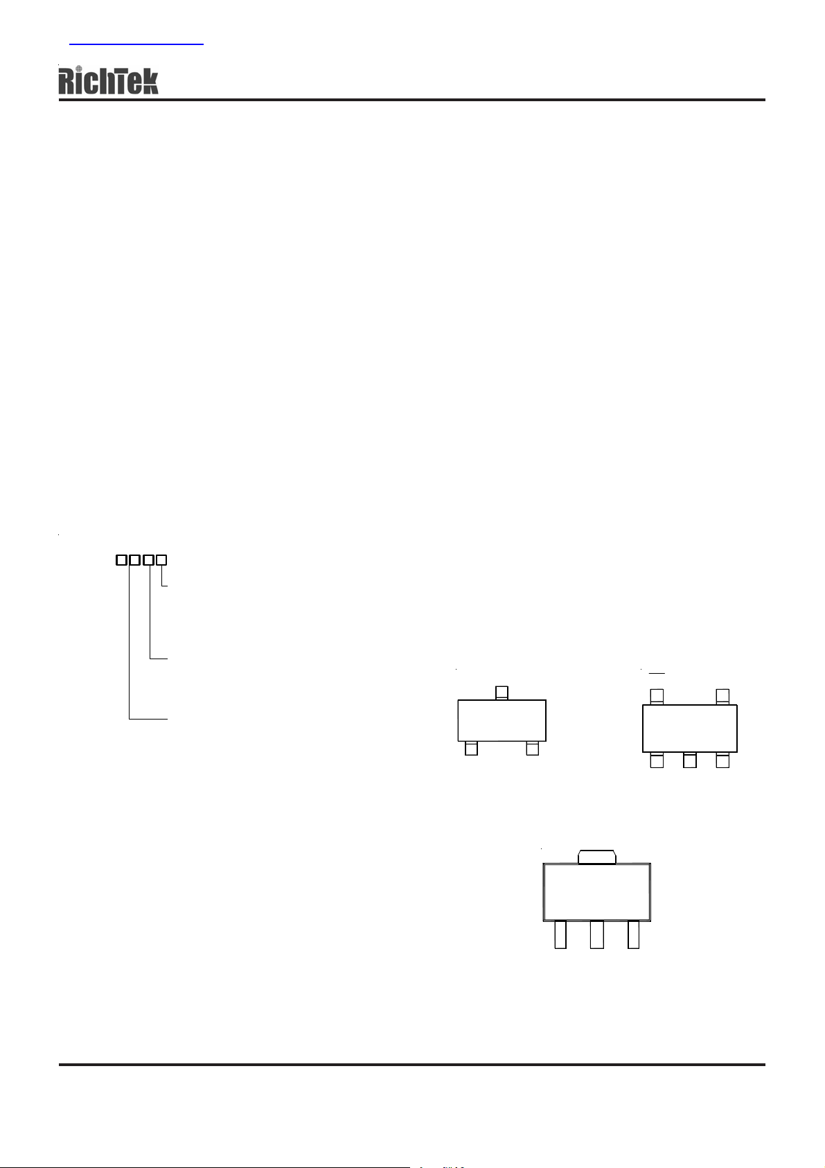
Pin Configurations
µµ
µF Output Capacitor Required for Stability
µµ
(TOP VIEW)
VIN
3
1
GND VOUT
2
SOT-23-3
231
EN
54
23
1
GND
VIN VOUT
SOT-23-5
µµ
µA)
µµ
NC
VIN
Marking Information
For marking information, contact our sales re presentative
GND VOUT
(TAB)
SOT-89
directly or through a RichTek distributor located in your
area, otherwise visit our website for detail.
DS9170-08 March 2005 www.richtek.com
1
Page 2
RT9170
Typical Application Circuit
Preliminary
V
IN
C
IN
1uF
Chip Enable
VIN
RT9170- CB
EN
Functional Pin Description
Pin No.
RT9170-CV RT9170-CB RT9170-CX
3 2 2 VIN Power Input Voltage
2 3 3 VOUT Output Voltage
1 1 1 GND Ground
- 5 -
- 4 - NC No Connection
Function Block Diagram
VOUT
GND
C
OUT
1uF
V
OUT
Pin Name Pin Function
EN
Chip Enable (Active Low)
EN
VIN
+
-
Current Limit
&
Thermal Shutdown
VOUT
GND
DS9170-08 March 2005www.richtek.com
2
Page 3
Preliminary
RT9170
Absolute Maximum Ratings (Note 1)
z Supply Input V oltage-------------------------------------------------------------------------------------------------- 7V
z Power Dissipation, P
D
@ T
= 25°C
A
SOT-23-3 ---------------------------------------------------------------------------------------------------------------- 0.4W
SOT-23-5 ---------------------------------------------------------------------------------------------------------------- 0.4W
SOT-89 ------------------------------------------------------------------------------------------------------------------- 0.571W
z Package Thermal Resistance (Note 7)
SOT-23-3, θJA---------------------------------------------------------------------------------------------------------- 250°C/W
SOT-23-5, θJA---------------------------------------------------------------------------------------------------------- 250°C/W
SOT-89, θJA------------------------------------------------------------------------------------------------------------- 175°C/W
z Junction Temperature------------------------------------------------------------------------------------------------ 150°C
z Storage Temperature Range--------------------------------------------------------------------------------------- −65°C to 150°C
z ESD Susceptibility (Note 2)
HBM (Human Body Mode) ----------------------------------------------------------------------------------------- 2kV
MM (Machine Mode) ------------------------------------------------------------------------------------------------- 200V
Recommended Operating Conditions (Note 3)
z Supply Input Voltage ------------------------------------------------------------------------------------------------- 2V to 5.5V
z Enable Input Voltage ------------------------------------------------------------------------------------------------- 0V to 5.5V
z Junction Temperature Range -------------------------------------------------------------------------------------- −40°C to 125°C
Electrical Characteristics
(V
= V
IN
+ 1V, CIN = C
OUT
OUT
= 1µF, T
Parameter Symbol Test Conditions Min Typ Max Units
Output Voltage Accuracy
Current Limit
Quiescent Current (Note 5)
Dropout Voltage
Line Regulation
Load Regulation (Note 4)
Standby Current (Note 6) I
Logic-Low Voltage
EN Threshold
Logic-Hi gh Voltage
Power Supply Rejection PSRR
Thermal Shutdown Temperature
= 25°C, unless otherwise specified)
A
∆V
I
LIM
I
Q
V
DROP
∆V
∆V
STBY
V
IL
V
IH
T
SD
I
OUT
R
LINE
1mA < I
LOAD
V
V
= 1mA
OUT
= 1Ω
LOAD
≤ 0.6V,
V
EN
= 300mA -- 240 --
I
OUT
V
= (V
IN
I
= 1mA
OUT
V
≥ 2V (Shutdown), VIN = 5.5V
EN
= 2V to 5.5V, Enable
IN
= 2V to 5.5V, Shutdown
IN
f = 1kHz, C
-- 150 --
= 0mA
IOUT
+ 0.3V) to 5.5V,
OUT
< 300mA
OUT
= 1µF
OUT
−2
300 -- --
-- 15 --
-- +2 %
mA
µA
mV
−0.3
0.018 +0.3 %/V
-- 0.01 0.04 %/mA
-- 0.1 --
µA
-- -- 0.6
V
2 -- --
--
−40
-- dB
°C
DS9170-08 March 2005 www.richtek.com
3
Page 4

RT9170
Note 1. Stresses listed as the above "Absolute Maximum Ratings" may cause permanent damage to the device. These are for
stress ratings. Functional operation of the device at these or any other conditions beyond those indicated in the operational
sections of the specifications is not implied. Exposure to absolute maximum rating conditions for extended periods may
remain possibility to affect device reliability.
Note 2. Devices are ESD sensitive. Handling precaution recommended.
Note 3. The device is not guaranteed to function outside its operating conditions
Note 4. Regulation is measured at constant junction temperature by using a 20ms current pulse. Devices are tested for load
regulation in the load range from 1mA to 300mA.
Note 5. Quiescent, or ground current, is the difference between input and output currents. It is defined by I
load condition (I
current.
Note 6. Standby current is the input current drawn by a regulator when the output voltage is disabled by a shutdown signal
2V). It is measured with VIN = 5.5V.
(V
≥
EN
Note 7. θ
is measured in the natural convection at TA = 25°C on a low effective thermal conductivity test board of
JA
JEDEC 51-3 thermal measurement standard.
= 0mA). The total current drawn from the supply is the sum of the load current plus the ground pin
OUT
Preliminary
= IIN - I
Q
under no
OUT
DS9170-08 March 2005www.richtek.com
4
Page 5

Typical Operating Characteristics
Preliminary
RT9170
Temperature Stability
2.55
2.53
2.51
2.49
2.47
2.45
2.43
2.41
Output Voltage (V)1
VIN = 3.5V
V
2.39
2.37
2.35
= 2.5V
OUT
C
= 1uF (Ceramic)
IN
C
= 1uF (Ceramic)
OUT
-35 -15 5 25 45 65 85 105 125
Temperature
I
LOAD
No Load
= 250mA
(°C)
Quiescent Current vs. Temperature
18
16
14
12
10
Quiescent Current (uA) 1
I
= 200mA
LOAD
No Load
8
6
VIN = 3.5V
4
2
0
= 2.5V
V
OUT
C
= 1uF (Ceramic)
IN
C
= 1uF (Ceramic)
OUT
-35 -15 5 25 45 65 85 105 125
Temperature
(°C)
Quiescent Current vs. Load Current
18
17
16
15
14
13
VIN = 3.5V
12
V
= 2.5V
OUT
Quiescent Current (uA) 1
C
= 1uF (Ceramic)
IN
11
C
= 1uF (Ceramic)
OUT
10
0 0.05 0.1 0.15 0.2 0.25 0.3
Load Current (A)
Quiescent Current vs. Supply Voltage
18
16
14
12
10
8
6
4
Quiescent Current (uA) 1
2
0
I
= 200mA
LOAD
V
= 2.5V
OUT
= 1uF (Ceramic)
C
IN
C
= 1uF (Ceramic)
OUT
22.533.544.555.5
Supply Vol tage (V)
No Load
Dropout Voltage vs. Load Current
300
V
= 3.3V
OUT
250
TJ = 125°C
200
TJ = 25°C
150
100
Dropout Voltage (mV)
50
0
0 0.05 0.1 0.15 0.2 0.25 0.3
Load Current (A)
TJ = -40°C
Output Voltage (V)1
2.55
2.53
2.51
2.49
2.47
2.45
Output Voltage vs. Supply Voltage
V
= 2.5V
OUT
C
= 1uF (Ceramic)
IN
C
= 1uF (Ceramic)
OUT
= 1mA
I
LOAD
2.5 3 3.5 4 4.5 5 5.5
Suppl y Voltage (V)
DS9170-08 March 2005 www.richtek.com
5
Page 6

RT9170
Preliminary
Load Regulation Deviation vs. Temperature
0
-0.0005
-0.001
-0.0015
-0.002
-0.0025
-0.003
-0.0035
-0.004
Load Regulation Deviation (%/mA)
-0.0045
V
= 2.5V
OUT
-35 -15 5 25 45 65 85 105 125
Temperature
(°C)
PSRR
0
PSRR(dB)1
-10
-20
-30
-40
-50
-60
VIN = 3.5V
= 2.5V
V
OUT
C
= 1uF (Ceramic)
OUT
I
LOAD
= 10mA
I
LOAD
= 250mA
Current Lim it vs . Te m pe rature
1.60
1.40
1.20
1.00
Current Limit (A)
0.80
VIN = 5V
V
= 3.3V
OUT
= 1Ω
R
0.60
L
-50-250 255075100125
Temperature
(°C)
Current Limit
C
= 10uF (Ceramic) X5R
IN
C
3.0
2.5
2.0
1.5
1.0
Current Limit (A)
0.5
0
= 10uF (Ceramic) X5R
OUT
V
= 5V
IN
= 1Ω
R
L
-70
10 100 1K 10K 100K 1M
Time (5ms/Div)
Frequency (Hz)
Output Voltage (V)
EN Voltage (V)
6
4
2
0
2
0
VIN = 5V
V
C
C
I
LOAD
= 3.3V
OUT
= 1uF (Ceramic)
IN
= 1uF (Ceramic)
OUT
= 300mA
Enable Re spone
Time (25ms/DIV)
Output Voltage (V)
EN Voltage (V)
3
2
1
0
2
1
0
Enable Re spone
VIN = 5V
V
OUT
= 1uF(Ceramic)
C
IN
C
OUT
I
LOAD
Time (5ms/Div)
= 3.3V
= 1uF(Ceramic)
= 300mA
DS9170-08 March 2005www.richtek.com
6
Page 7

Preliminary
RT9170
VIN = 3.5V, V
T
250
0
Load Current (mA)
≈
200
0
-200
Output Voltage
Deviation (mV)
VIN = 3.5V, V
I
300
200
100
Load T ra n sient Re spon se
= 2.5V
OUT
= 25°C
A
Time (0.5ms/Div)
Noise
= 2.5V
OUT
= 250mA
OUT
C
= 1uF (Ceramic)
IN
C
= 1uF (Ceramic)
OUT
C
= 1uF (Ceramic)
IN
C
= 1uF (Ceramic)
OUT
Line Tra n sient Response
6
V
= 2.5V
OUT
T
= 25°C
A
5
4
3
Deviation (V)
Input Voltage
≈
Output Voltage
≈
100
0
-100
Deviation (mV)
Time (0.5ms/Div)
C
= 1uF (Ceramic)
OUT
= 250mA
I
OUT
≈
0
Noise(uV)
-100
-200
-300
Times (2.5ms/Div)
DS9170-08 March 2005 www.richtek.com
7
Page 8

RT9170
Preliminary
Application Information
Like any low-dropout regulator , the RT9170 requires input
and output decoupling ca pacitors. The device is specifically
designed for portable a pplications requiring minimum board
space a nd smallest components. These capacitors must
be correctly selected for good performa nce (see Capa citor
Characteristics Section). Plea se note that linear regulators
with a low dropout voltage have high internal loop gains
which require care in guarding against oscillation caused
by insufficient decoupling ca pa citance.
Input Capacitor
An input capacitance of 1µF is required between the
device input pin and ground directly (the amount of the
capacitance may be increased without limit). The input
cap acitor MUST be located less than 1 cm from the device
to assure in put stability (see PCB Layout Section). A lower
ESR capacitor allows the use of less capacitance, while
higher ESR type (like aluminum electrolytic) require more
capacitance.
Cap acitor types (aluminum, cera mic and ta ntalum) can be
mixed in parallel, but the total equivalent input cap acitance/
ESR must be defined a s above to stable operation.
There are no requirements for the ESR on the input
cap acitor , but tolera nce and te mperature coefficient must
be considered when selecting the ca pacitor to ensure the
capacitance will be 1µF over the entire operating
temperature range.
Output Capa citor
The RT9170 is designed specifically to work with very
small ceramic output capacitors. A ceramic capacitor
(temperature characteristics X7R, X5R, Z5U, or Y5V) in
1µF to 10µF with 5mΩ to 50mΩ range is suitable for the
RT9170 application. The recommended minimum
capacitance for the device is 1µF, X5R or X7R dielectric
ceramic, between V
be increased without li mit. Higher ca pacita nce values help
to improve tran sient.
The output capacitor's ESR is critical because it forms a
zero to provide phase lead which is required for loop
stability.
≅
≅
and GND for stability, but it may
OUT
No Load Stability
The device will remain stable and in regulation with no
external load. This is specially i mport in CMOS RAM keepalive applications
Input-Output (Dropout) V olatge
A regulator's minimum input-to-output voltage differential
(dropout voltage) determines the lowest usable supply
voltage. In battery-powered systems, this determines the
useful end-of-life battery voltage. Because the device uses
a PMOS, its dropout voltage is a function of drain-tosource on-resistance, R
, multiplied by the load
DS(ON)
current:
V
DROPOUT
= VIN -V
OUT
= R
DS(ON)
x I
OUT
Current Limit
The RT9170 monitors and controls the PMOS' gate voltage,
limiting the output current to 0.3A (min). The output can
be shorted to ground for an indefinite period of ti me without
damaging the part.
Short-Circuit Protection
The device is short circuit protected and in the event of a
peak over-current condition, the short-circuit control loop
will rapidly drive the output PMOS pa ss element of f. Once
the power pass element shuts down, the control loop will
rapidly cycle the output on a nd off until the average power
dissipation causes the thermal shutdown circuit to
respond to servo the on/off cycling to a lower frequency.
Please refer to the section on thermal information for
power dissipation calculations.
Cap acitor Characteristics
It is important to note that capacitance tolerance and
variation with temperature must be taken into consideration
when selecting a cap a citor so that the mini mum required
a mount of ca p a cita nce is provided over the full operating
temperature range. In general, a good ta ntalum cap acitor
will show very little cap acitance vari ation with temperature,
but a ceramic may not be a s good (depending on dielectric
type).
DS9170-08 March 2005www.richtek.com
8
Page 9

Preliminary
RT9170
Aluminum electrolytics also typically have large
temperature variation of ca pacita nce value.
Equally important to con sider is a capa citor's ESR change
with temperature: this is not an issue with ceramics, as
their ESR is extremely low. However, it is very important
in Tantalum and aluminum electrolytic capacitors. Both
show increasing ESR at colder temperatures, but the
increa se in aluminum electrolytic capacitors is so severe
they may not be feasible for some applications.
Ceramic:
For values of capacitance in the 10µF to 100µF range,
ceramics are usually larger and more costly than
tantalums but give superior AC performance for bypassing high frequency noise because of very low ESR
(typically less than 10mΩ). However , some dielectric types
do not have good cap acitance chara cteristics a s a function
of voltage and temperature.
Z5U and Y5V dielectric ceramics have capacitance that
drops severely with applied voltage. A typical Z5U or Y5V
capacitor can lose 60% of its rated capacitance with half
of the rated voltage applied to it. The Z5U and Y5V also
exhibit a severe temperature effect, losing more than 50%
of nominal capacitance at high and low limits of the
temperature range.
X7R and X5R dielectric ceramic capacitors are strongly
recommended if ceramics are used, as they typically
maintain a capa citance ra nge within ±20% of nominal over
full operating ratings of temperature and voltage. Of
course, they are typically larger and more costly than
Z5U/Y5U types for a given voltage and capacitance.
Tantalum:
Solid tantalum capacitors are recommended for use on
the output because their typical ESR is very close to the
ideal value required for loop compensation. They also
work well as in put ca p a citors if selected to meet the ESR
requirements previously listed.
Tantalums also have good temperature stability: a good
quality tantalum will typically show a capacitance value
that varies less than 10-15% across the full temperature
range of 125°C to -40°C. ESR will vary only about 2X
going from the high to low temperature limits.
The increasing ESR at lower temperatures can cause
oscillations when marginal quality ca pa citors are used (if
the ESR of the capacitor is near the upper limit of the
stability range at room temperature).
Aluminum:
This capacitor type offers the most capacitance for the
money. The disadvantages are that they are larger in
physical size, not widely available in surface mount, and
have poor AC performance (especially at higher
frequencies) due to higher ESR and ESL.
Compared by size, the ESR of an aluminum electrolytic
is higher than either Tantalum or cera mic, and it also varies
greatly with temperature. A typical aluminum electrolytic
can exhibit an ESR increase of as much as 50X when
going from 25°C down to -40°C.
It should also be noted that many aluminum electrolytics
only specify impedance at a frequency of 120Hz, which
indicates they have poor high frequency performance.
Only aluminum electrolytics that have an impedance
specified at a higher frequency (between 20kHz and
100kHz) should be used for the device. Derating must be
applied to the manufacturer's ESR specification, since it
is typically only valid at room temperature.
Any application s using aluminum electrolytics should be
thoroughly tested at the lowest ambient operating
temperature where ESR is maximum.
Thermal Considerations
The RT9170 series can deliver a current of up to 300mA
over the full operating junction temperature range. However ,
the maximum output current must be derated at higher
ambient temperature to ensure the junction temperature
does not exceed 125°C. With all possible conditions, the
junction temperature must be within the range specified
under operating conditions. Power dissipation can be
calculated based on the output current and the voltage
drop across regulator .
PD = (V
- V
) I
IN
OUT
OUT
+ VIN I
GND
DS9170-08 March 2005 www.richtek.com
9
Page 10

RT9170
Preliminary
The final operating junction temperature for any set of
conditions can be estimated by the following thermal
equation:
P
D (MAX)
Where T
= ( T
J (MAX)
J (MAX)
is the maximum junction temperature of
- T
A
) / θ
JA
the die (125°C) and TA is the maximum ambient
temperature. The junction to ambient thermal resistance
(θJA) for SOT -23-3 a nd SOT-23-5 packages at recommended
minimum footprint is 250°C/W, 175°C/W for SOT-89
package (θJA is layout dependent). Visit our website in
which “Recommended Footprints for Soldering Surface
Mount Packages” for detail.
PCB Layout
Good board layout practices must be used or instability
can be induced because of ground loops and voltage
drops. The input and output capacitors MUST be directly
connected to the input, output, and ground pins of the
device using traces which have no other currents flowing
through them.
The best way to do this is to layout C
device with short traces to the VIN, V
and C
IN
, and ground pins.
OUT
near the
OUT
The regulator ground pin should be connected to the
external circuit ground so that the regulator and its
capacitors have a “single point ground”.
EN
GND
NC
VOUT
VIN
SOT-23-5 Board Layout
It should be noted that stability problems have been seen
in applications where “vias” to an internal ground plane
were used at the ground points of the device and the
input and output capacitors. This was caused by varying
ground potentials at these nodes resulting from current
flowing through the ground plane. Using a single point
ground technique for the regulator and it's ca pa citors fixed
the problem. Since high current flows through the traces
going into V
and coming from V
IN
, Kelvin connect the
OUT
capacitor leads to these pins so there is no voltage drop
in series with the input and output capacitors.
Optimum performance can only be achieved when the
device is mounted on a PC board according to the diagra m
below:
10
DS9170-08 March 2005www.richtek.com
Page 11

Outline Dimension
Preliminary
RT9170
D
C
e
A
b
Dimensions In M illimeters Dimensions In Inches
Symbol
Min Max Min Max
A 0.889 1.295 0.035 0.051
A1 0.000 0.152 0.000 0.006
B
A1
H
L
B 1.397 1.803 0.055 0.071
b 0.356 0.508 0.014 0.020
C 2.591 2.997 0.102 0.118
D 2.692 3.099 0.106 0.122
e 1.803 2.007 0.071 0.079
H 0.080 0.254 0.003 0.010
L 0.300 0.610 0.012 0.024
SOT-23-3 Surface Mount Package
DS9170-08 March 2005 www.richtek.com
11
Page 12

RT9170
Preliminary
H
D
L
C
b
A
e
Dimensions In Millimeters Dimensions In Inches
Symbol
Min Max Min Max
A 0.889 1.295 0.035 0.051
A1 0.000 0.152 0.000 0.006
B 1.397 1.803 0.055 0.071
b 0.356 0.559 0.014 0.022
C 2.591 2.997 0.102 0.118
D 2.692 3.099 0.106 0.122
B
A1
12
e 0.838 1.041 0.033 0.041
H 0.080 0.254 0.003 0.010
L 0.300 0.610 0.012 0.024
SOT-23-5 Surface Mount Package
DS9170-08 March 2005www.richtek.com
Page 13

Preliminary
D
D1
RT9170
A
C
B
C1
e
e
H
A
b
b1
Dimensions In Millimeters Dimensions In Inches
Symbol
Min Max Min Max
A 1.397 1.600 0.055 0.063
b 0.356 0.483 0.014 0.019
B 2.388 2.591 0.094 0.102
b1 0.406 0.533 0.016 0.021
b
C 3.937 4.242 0.155 0.167
C1 0.787 1.194 0.031 0.047
D 4.394 4.597 0.173 0.181
D1 1.397 1.753 0.055 0.069
e 1.448 1.549 0.057 0.061
H 0.356 0.432 0.014 0.017
3-Lead SOT-89 Surface Mount Package
RICHTEK TECHNOLOGY CORP .
Headquarter
5F, No. 20, Taiyuen Street, Chupei City
Hsinchu, Taiwan, R.O.C.
Tel: (8863)5526789 Fax: (8863)5526611
RICHTEK TECHNOLOGY CORP .
Ta ipei Office (Marketing)
8F-1, No. 137, Lane 235, Paochiao Road, Hsintien City
Ta ipei County, Taiwan, R.O.C.
Tel: (8862)89191466 Fax: (8862)89191465
Email: marketing@richtek.com
DS9170-08 March 2005 www.richtek.com
13
 Loading...