

Page 1
Data Sheet D8953BDSB
March 30, 1999
RS8953B/8953SPB
HDSL Channel Unit
The RS8953B is a High-Bit-Rate Digital Subscriber Line (HDSL) channel unit designed
to perform data, clock, and format conversions necessary to construct a Pulse Code
Multiplexed (PCM) channel from one, two, or three HDSL channels. The PCM channel
consists of transmit and receive data, clock and frame sync signals configured for
standard T1 (1544 kbps), standard E1 (2048 kbps), or custom (Nx64 kbps) formats.
The PCM channel connects directly to a Bt8370 T1/E1 Controller or similar T1/E1 device.
Connection to other network/subscriber physical layer devices is supported by the
custom PCM frame format. Three identical HDSL channel interfaces consist of serial
data and clock connected to a Bt8970 HDSL Transceiver or similar 2B1Q bit pump
device. The RS8953SPB contains one HDSL channel interface.
Control and status registers are accessed via the Microprocessor Unit (MPU)
interface. One common register group configures the PCM interface formatter,
Pseudo-Random Bit Sequence (PRBS) generator, Bit Error Rate (BER) meter, timeslot
router, Digital Phase Lock Loop (DPLL) clock recovery, and PCM Loopbacks (LB). Three
groups of HDSL channel registers configure the elastic store FIFOs, overhead MUXes,
receive framers, payload mappers, and HDSL loopbacks. Status registers monitor
received overhead, DPLL, FIFO, and framer operations, including CRC and FEBE error
counts.
The RS8953B adheres to Bellcore TA-NWT-001210 and FA-NWT-001211 and the
latest ETSI RTR/TM-03036 standards. C-language software for all standard T1/E1
configuration and startup procedures is implemented on Conexant's HDSL Evaluation
Module (Bt8973EVM) and is available under a no-fee license agreement. RS8953B
software can also be developed for non-standard HDSL applications or to interoperate
with existing HDSL equipment.
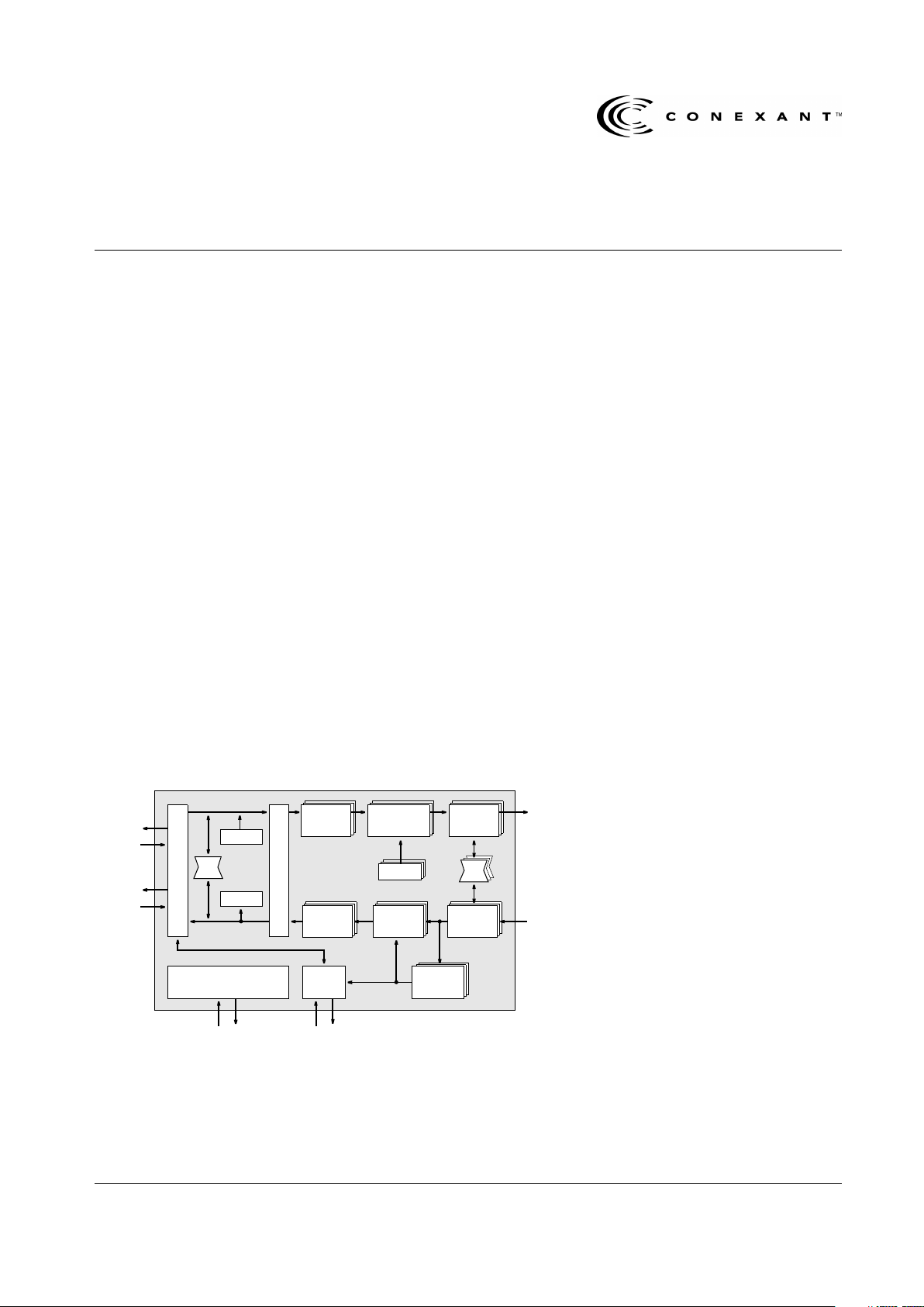
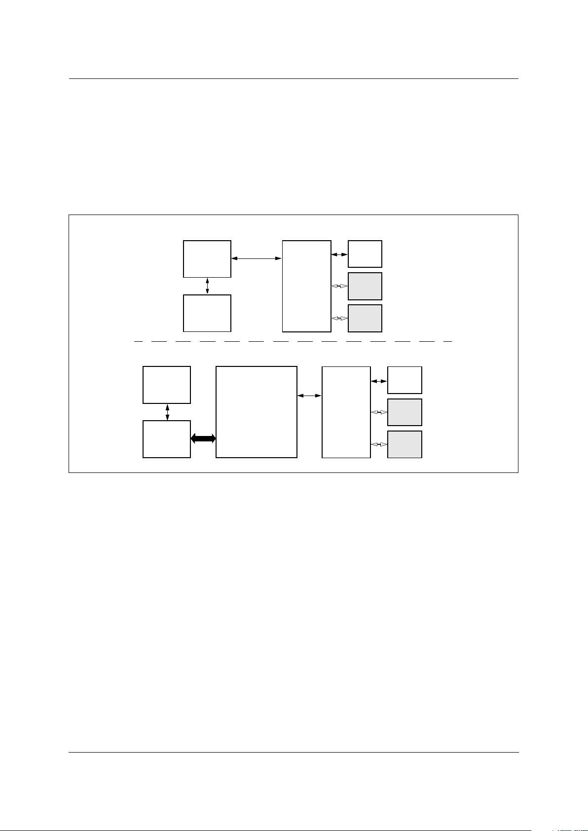
Functional Block Diagram
Distinguishing Features
• Supports All HDSL Bit Rates
– 2 pair T1 standard (784 kbps)
– 2 pair E1 standard (1168 kbps)
– 3 pair E1 standard (784 kbps)
– 1/2/3 pair custom (Nx64 kbps,
N=2-36)
• T1/E1 Primary Rate (PCM) Channel
– Connects to Conexant E1/T1
Framers
– Framed or unframed mode
– Sync/Async payload mapping
– Clock recovery/jitter attenuation
– PRBS/fixed test patterns
– BER measurement
• HDSL Channels
– Connects to Conexant ZipWire
Transceivers
– Three independent serial channels
– Central, remote, or repeater
– Overhead (HOH) management
– Programmable path delays
– Error performance monitoring
– Software controlled EOC and IND
– Auxiliary payload/Z-bit data link
– Master loop ID and interchange
– Auto tip/ring reversal
• Programmable Data Routing
– PCM timeslots – HDSL payload
– Drop/Insert – HDSL payload
– Auxiliary – HDSL payload
– PRBS/Fixed – PCM or HDSL
– PCM and HDSL loopbacks
•Intel
®
or Motorola® MPU interface
• CMOS technology, 3.3 V operation
• 68-pin PLCC or 80-pin PQFP
Applications
• Full, Fractional or Multipoint T1/E1
• Single and Multichannel Repeaters
• Voice Pair Gain Systems
• Wireless LAN/PBX
• PCS, Cellular Base Station
• Fiber Access/Distribution
• Loop Carrier, Remote Switches
• Subscriber Line Modem
MPU
Registers
DPLL
Receive
Framer
Payload
Mapper
Elastic
Store
Stuff
2B1Q
Decoder
LB
Mapper
HOH Mux
2B1Q
Encoder
Elastic
Store
LB
PRBS
BER
PCM Formatter
Timeslot Router
HDSL
Channels
1, 2, 3
Drop
Insert
PCM
Channel
Microprocessor
PLL Filter
Page 2

D8953BDSB Conexant
Information provided by Conexant Syste ms, Inc. (Conexant) is believed to be accurate and reliable. However, no responsibility is
assumed by Conexant for its use, nor any infringement of patents or other rights of third parties which may result from its use. No
license is granted by implication or otherwise under any patent rights of Conexant other than for circuitry embodied in Conexant
products. Conexant reserves the right to change circuitry at any time without notice. This document is subject to change without
notice.
Conexant and “What’s Next in Communications Technologies” are trademarks of Conexant Systems, Inc.
Product names or services listed in this publication are for identification purposes only, and may be trademarks or registered
trademarks of their respective companies. All other marks mentioned herein are the property of their respective holders.
© 1999 Conexant Systems, Inc.
Print ed in U.S.A.
All Rights Reserved
Reader Response:
To improve the qu ali ty o f our publicatio ns, we welcome your feedback. Please send c om me nts or
suggestions via e-mail to Conexant Reader Response@conexant.com. Sorry, we can't answer your technical
questions at this address. Please contact your local Conexant sales office or local field applications engineer if you
have technical questions.
Ordering Information
Order Number Package
Number of
HDSL Channels
Operating Temperature Range
RS8953BEPF 80–Pin Plastic Quad Flat Pack (PQFP) 3 –40°C to +85°C
RS8953BEPJ 68–Pin Plastic Leaded Chip Carrier (PLCC) 3 –40°C to +85°C
RS8953SPB EPF 80–Pin Plastic Quad Flat Pack (PQFP) 1 –40°C to +85°C
RS8953SPB EPJ 68–Pin Plastic Leaded Chip Carrier (PLCC) 1 –40°C to +85°C
Page 3

N8953BDSB Conexant iii
Table of Contents
List of Figures
. . . . . . . . . . . . . . . . . . . . . . . . . . . . . . . . . . . . . . . . . . . . . . . . . . . . . . . . . . . . . . . . . . . . . . . . . xi
List of Tables
. . . . . . . . . . . . . . . . . . . . . . . . . . . . . . . . . . . . . . . . . . . . . . . . . . . . . . . . . . . . . . . . . . . . . . . . . xiii
1.0 HDSL Systems
. . . . . . . . . . . . . . . . . . . . . . . . . . . . . . . . . . . . . . . . . . . . . . . . . . . . . . . . . . . . . . . . . 1-1
1.1 HTU Applications
. . . . . . . . . . . . . . . . . . . . . . . . . . . . . . . . . . . . . . . . . . . . . . . . . . . . . . . . . . . 1-1
1.1.1 Repeaters
. . . . . . . . . . . . . . . . . . . . . . . . . . . . . . . . . . . . . . . . . . . . . . . . . . . . . . . . . . . 1-2
1.1.2 Fractional Transport
. . . . . . . . . . . . . . . . . . . . . . . . . . . . . . . . . . . . . . . . . . . . . . . . . . . . 1-3
1.1.3 Switching Systems
. . . . . . . . . . . . . . . . . . . . . . . . . . . . . . . . . . . . . . . . . . . . . . . . . . . . . 1-4
1.1.4 Loop Carrier/Pair Gain
. . . . . . . . . . . . . . . . . . . . . . . . . . . . . . . . . . . . . . . . . . . . . . . . . . 1-5
1.1.5 Point-to-Multipoint
. . . . . . . . . . . . . . . . . . . . . . . . . . . . . . . . . . . . . . . . . . . . . . . . . . . . . 1-6
1.1.6 Subscriber Modem
. . . . . . . . . . . . . . . . . . . . . . . . . . . . . . . . . . . . . . . . . . . . . . . . . . . . . 1-7
1.2 System Interfaces
. . . . . . . . . . . . . . . . . . . . . . . . . . . . . . . . . . . . . . . . . . . . . . . . . . . . . . . . . . . 1-8
2.0 Pin Descriptions
. . . . . . . . . . . . . . . . . . . . . . . . . . . . . . . . . . . . . . . . . . . . . . . . . . . . . . . . . . . . . . . . 2-1
2.1 Pin Assignments
. . . . . . . . . . . . . . . . . . . . . . . . . . . . . . . . . . . . . . . . . . . . . . . . . . . . . . . . . . . . 2-1
2.2 Signal Definitions
. . . . . . . . . . . . . . . . . . . . . . . . . . . . . . . . . . . . . . . . . . . . . . . . . . . . . . . . . . . 2-7
3.0 Circuit Descriptions
. . . . . . . . . . . . . . . . . . . . . . . . . . . . . . . . . . . . . . . . . . . . . . . . . . . . . . . . . . . . . 3-1
3.1 MPU Interface
. . . . . . . . . . . . . . . . . . . . . . . . . . . . . . . . . . . . . . . . . . . . . . . . . . . . . . . . . . . . . . 3-1
3.1.1 Address/Data Bus
. . . . . . . . . . . . . . . . . . . . . . . . . . . . . . . . . . . . . . . . . . . . . . . . . . . . . . 3-2
3.1.2 Bus Controls
. . . . . . . . . . . . . . . . . . . . . . . . . . . . . . . . . . . . . . . . . . . . . . . . . . . . . . . . . 3-2
3.1.3 Interrupt Request
. . . . . . . . . . . . . . . . . . . . . . . . . . . . . . . . . . . . . . . . . . . . . . . . . . . . . . 3-3
3.1.4 Hardware Reset
. . . . . . . . . . . . . . . . . . . . . . . . . . . . . . . . . . . . . . . . . . . . . . . . . . . . . . . 3-3
3.2 PCM Channel
. . . . . . . . . . . . . . . . . . . . . . . . . . . . . . . . . . . . . . . . . . . . . . . . . . . . . . . . . . . . . . 3-4
3.2.1 PCM Transmit
. . . . . . . . . . . . . . . . . . . . . . . . . . . . . . . . . . . . . . . . . . . . . . . . . . . . . . . . 3-5
3.2.1.1 Transmit Synchronization
. . . . . . . . . . . . . . . . . . . . . . . . . . . . . . . . . . . . . . . 3-6
3.2.1.2 Transmit Routing Table
. . . . . . . . . . . . . . . . . . . . . . . . . . . . . . . . . . . . . . . . . 3-7
3.2.1.3 PRBS Generator
. . . . . . . . . . . . . . . . . . . . . . . . . . . . . . . . . . . . . . . . . . . . . . 3-7
3.2.1.4 Drop/Insert Channel
. . . . . . . . . . . . . . . . . . . . . . . . . . . . . . . . . . . . . . . . . . . 3-8
3.2.1.5 TFIFO Water Levels
. . . . . . . . . . . . . . . . . . . . . . . . . . . . . . . . . . . . . . . . . . . . 3-9
3.2.2 PCM Receive
. . . . . . . . . . . . . . . . . . . . . . . . . . . . . . . . . . . . . . . . . . . . . . . . . . . . . . . . 3-10
Page 4

Table of Contents
RS8953B/8953SPB
HDSL Channel Unit
iv Conexant N8953BDSB
3.2.2.1 Receive Synchronization
. . . . . . . . . . . . . . . . . . . . . . . . . . . . . . . . . . . . . . . 3-12
3.2.2.2 Receive Combination Table
. . . . . . . . . . . . . . . . . . . . . . . . . . . . . . . . . . . . . 3-12
3.2.2.3 BER Meter
. . . . . . . . . . . . . . . . . . . . . . . . . . . . . . . . . . . . . . . . . . . . . . . . . 3-13
3.2.2.4 RFIFO Water Level
. . . . . . . . . . . . . . . . . . . . . . . . . . . . . . . . . . . . . . . . . . . . 3-14
3.3 Clock Recovery DPLL
. . . . . . . . . . . . . . . . . . . . . . . . . . . . . . . . . . . . . . . . . . . . . . . . . . . . . . . 3-15
3.4 Loopbacks
. . . . . . . . . . . . . . . . . . . . . . . . . . . . . . . . . . . . . . . . . . . . . . . . . . . . . . . . . . . . . . . . 3-17
3.5 HDSL Channel
. . . . . . . . . . . . . . . . . . . . . . . . . . . . . . . . . . . . . . . . . . . . . . . . . . . . . . . . . . . . . 3-19
3.5.1 HDSL Transmit
. . . . . . . . . . . . . . . . . . . . . . . . . . . . . . . . . . . . . . . . . . . . . . . . . . . . . . . 3-24
3.5.1.1 Transmit Payload Mapper
. . . . . . . . . . . . . . . . . . . . . . . . . . . . . . . . . . . . . . 3-24
3.5.1.2 HOH Multiplexer
. . . . . . . . . . . . . . . . . . . . . . . . . . . . . . . . . . . . . . . . . . . . . 3-24
3.5.1.3 CRC Calculation
. . . . . . . . . . . . . . . . . . . . . . . . . . . . . . . . . . . . . . . . . . . . . 3-25
3.5.1.4 Scrambler
. . . . . . . . . . . . . . . . . . . . . . . . . . . . . . . . . . . . . . . . . . . . . . . . . . 3-25
3.5.1.5 STUFF Generator
. . . . . . . . . . . . . . . . . . . . . . . . . . . . . . . . . . . . . . . . . . . . . 3-25
3.5.1.6 2B1Q Encoder
. . . . . . . . . . . . . . . . . . . . . . . . . . . . . . . . . . . . . . . . . . . . . . . 3-26
3.5.1.7 HDSL Auxiliary Transmit
. . . . . . . . . . . . . . . . . . . . . . . . . . . . . . . . . . . . . . . 3-27
3.5.2 HDSL Receive
. . . . . . . . . . . . . . . . . . . . . . . . . . . . . . . . . . . . . . . . . . . . . . . . . . . . . . . 3-28
3.5.2.1 2B1Q Decoder
. . . . . . . . . . . . . . . . . . . . . . . . . . . . . . . . . . . . . . . . . . . . . . . 3-28
3.5.2.2 HDSL Receive Framer
. . . . . . . . . . . . . . . . . . . . . . . . . . . . . . . . . . . . . . . . . 3-29
3.5.2.3 Descrambler
. . . . . . . . . . . . . . . . . . . . . . . . . . . . . . . . . . . . . . . . . . . . . . . . 3-31
3.5.2.4 CRC Checking
. . . . . . . . . . . . . . . . . . . . . . . . . . . . . . . . . . . . . . . . . . . . . . . 3-32
3.5.2.5 HOH Demux
. . . . . . . . . . . . . . . . . . . . . . . . . . . . . . . . . . . . . . . . . . . . . . . . 3-32
3.5.2.6 Receive Payload Mapper
. . . . . . . . . . . . . . . . . . . . . . . . . . . . . . . . . . . . . . . 3-32
3.5.2.7 HDSL Auxiliary Receive
. . . . . . . . . . . . . . . . . . . . . . . . . . . . . . . . . . . . . . . . 3-32
3.6 PRA Function
. . . . . . . . . . . . . . . . . . . . . . . . . . . . . . . . . . . . . . . . . . . . . . . . . . . . . . . . . . . . . 3-34
3.6.1 Transferring Data from HDSL to RSER
. . . . . . . . . . . . . . . . . . . . . . . . . . . . . . . . . . . . . 3-34
3.6.2 Definitions of Detection Algorithms
. . . . . . . . . . . . . . . . . . . . . . . . . . . . . . . . . . . . . . . . 3-35
3.6.3 Inserting Data Transferred from HDSL to RSER
. . . . . . . . . . . . . . . . . . . . . . . . . . . . . . . 3-35
3.6.4 Transferring Data from TSER to HDSL
. . . . . . . . . . . . . . . . . . . . . . . . . . . . . . . . . . . . . . 3-35
3.6.5 Inserting Data Transferred from TSER to HDSL
. . . . . . . . . . . . . . . . . . . . . . . . . . . . . . . 3-36
4.0 Registers
. . . . . . . . . . . . . . . . . . . . . . . . . . . . . . . . . . . . . . . . . . . . . . . . . . . . . . . . . . . . . . . . . . . . . . 5-1
4.1 Address Map
. . . . . . . . . . . . . . . . . . . . . . . . . . . . . . . . . . . . . . . . . . . . . . . . . . . . . . . . . . . . . . . 5-3
4.2 HDSL Transmit
. . . . . . . . . . . . . . . . . . . . . . . . . . . . . . . . . . . . . . . . . . . . . . . . . . . . . . . . . . . . . 5-9
Page 5

RS8953B/8953SPB
Table of Contents
HDSL Channel Unit
N8953BDSB Conexant v
0x00—Transmit Embedded Operations Channel (TEOC_LO)
. . . . . . . . . . . . . . . . . . . . . 5-10
0x01—Transmit Embedded Operations Channel (TEOC_HI)
. . . . . . . . . . . . . . . . . . . . . . 5-10
0x02—Transmit Indicator Bits (TIND_LO)
. . . . . . . . . . . . . . . . . . . . . . . . . . . . . . . . . . . 5-10
0x03—Transmit Indicator Bits (TIND_HI)
. . . . . . . . . . . . . . . . . . . . . . . . . . . . . . . . . . . 5-10
0x04—Transmit Z-Bits (TZBIT_1)
. . . . . . . . . . . . . . . . . . . . . . . . . . . . . . . . . . . . . . . . . 5-10
0xDF—Transmit Z-Bits (TZBIT_2)
. . . . . . . . . . . . . . . . . . . . . . . . . . . . . . . . . . . . . . . . . 5-11
0xE0—Transmit Z-Bits (TZBIT_3)
. . . . . . . . . . . . . . . . . . . . . . . . . . . . . . . . . . . . . . . . . 5-11
0xE1—Transmit Z-Bits (TZBIT_4)
. . . . . . . . . . . . . . . . . . . . . . . . . . . . . . . . . . . . . . . . . 5-11
0xE2—Transmit Z-Bits (TZBIT_5)
. . . . . . . . . . . . . . . . . . . . . . . . . . . . . . . . . . . . . . . . . 5-11
0xE3—Transmit Z-Bits (TZBIT_6)
. . . . . . . . . . . . . . . . . . . . . . . . . . . . . . . . . . . . . . . . . 5-11
0x05—Transmit FIFO Water Level (TFIFO_WL)
. . . . . . . . . . . . . . . . . . . . . . . . . . . . . . . 5-12
0x06—Transmit Command Register 1 (TCMD_1)
. . . . . . . . . . . . . . . . . . . . . . . . . . . . . 5-12
0x07—Transmit Command Register 2 (TCMD_2)
. . . . . . . . . . . . . . . . . . . . . . . . . . . . . 5-13
4.3 Transmit Payload Mapper
. . . . . . . . . . . . . . . . . . . . . . . . . . . . . . . . . . . . . . . . . . . . . . . . . . . . 5-15
0x08—Transmit Payload Map (TMAP_1)
. . . . . . . . . . . . . . . . . . . . . . . . . . . . . . . . . . . 5-15
0x09—Transmit Payload Map (TMAP_2)
. . . . . . . . . . . . . . . . . . . . . . . . . . . . . . . . . . . 5-15
0x0A—Transmit Payload Map (TMAP_3)
. . . . . . . . . . . . . . . . . . . . . . . . . . . . . . . . . . . 5-15
0x0B—Transmit Payload Map (TMAP_4)
. . . . . . . . . . . . . . . . . . . . . . . . . . . . . . . . . . . 5-15
0x0C—Transmit Payload Map (TMAP_5)
. . . . . . . . . . . . . . . . . . . . . . . . . . . . . . . . . . . 5-15
0x0F—Transmit Payload Map (TMAP_6)
. . . . . . . . . . . . . . . . . . . . . . . . . . . . . . . . . . . . 5-16
0x10—Transmit Payload Map (TMAP_7)
. . . . . . . . . . . . . . . . . . . . . . . . . . . . . . . . . . . 5-16
0x11—Transmit Payload Map (TMAP_8)
. . . . . . . . . . . . . . . . . . . . . . . . . . . . . . . . . . . 5-16
0x12—Transmit Payload Map (TMAP_9)
. . . . . . . . . . . . . . . . . . . . . . . . . . . . . . . . . . . 5-16
0x0D—Transmit FIFO Reset (TFIFO_RST)
. . . . . . . . . . . . . . . . . . . . . . . . . . . . . . . . . . . 5-17
0x0E—Scrambler Reset (SCR_RST)
. . . . . . . . . . . . . . . . . . . . . . . . . . . . . . . . . . . . . . . 5-17
4.4 HDSL Receive
. . . . . . . . . . . . . . . . . . . . . . . . . . . . . . . . . . . . . . . . . . . . . . . . . . . . . . . . . . . . . 5-18
0x60—Receive Command Register 1 (RCMD_1)
. . . . . . . . . . . . . . . . . . . . . . . . . . . . . . 5-19
0x61—Receive Command Register 2 (RCMD_2)
. . . . . . . . . . . . . . . . . . . . . . . . . . . . . . 5-20
0x62—Receive Elastic Store FIFO Reset (RFIFO_RST)
. . . . . . . . . . . . . . . . . . . . . . . . . . 5-21
0x63—Receive Framer Synchronization Reset (SYNC_RST)
. . . . . . . . . . . . . . . . . . . . . 5-21
4.5 Receive Payload Mapper
. . . . . . . . . . . . . . . . . . . . . . . . . . . . . . . . . . . . . . . . . . . . . . . . . . . . 5-22
0x64—Receive Payload Map (RMAP_1)
. . . . . . . . . . . . . . . . . . . . . . . . . . . . . . . . . . . . 5-22
0x65—Receive Payload Map (RMAP_2)
. . . . . . . . . . . . . . . . . . . . . . . . . . . . . . . . . . . . 5-22
0x66—Receive Payload Map (RMAP_3)
. . . . . . . . . . . . . . . . . . . . . . . . . . . . . . . . . . . . 5-22
0x69—Receive Payload Map (RMAP_4)
. . . . . . . . . . . . . . . . . . . . . . . . . . . . . . . . . . . . 5-22
0x6A—Receive Payload Map (RMAP_5)
. . . . . . . . . . . . . . . . . . . . . . . . . . . . . . . . . . . . 5-22
0x6B—Receive Payload Map (RMAP_6)
. . . . . . . . . . . . . . . . . . . . . . . . . . . . . . . . . . . . 5-23
0x67—Error Count Reset (ERR_RST)
. . . . . . . . . . . . . . . . . . . . . . . . . . . . . . . . . . . . . . 5-23
0x68—Receive Signaling Location (RSIG_LOC)
. . . . . . . . . . . . . . . . . . . . . . . . . . . . . . 5-23
4.6 PCM Formatter
. . . . . . . . . . . . . . . . . . . . . . . . . . . . . . . . . . . . . . . . . . . . . . . . . . . . . . . . . . . . 5-25
0xC0—TSER Frame Bit Location (TFRAME_LOC_LO)
. . . . . . . . . . . . . . . . . . . . . . . . . . 5-26
0xC1—TSER Frame Bit Location (TFRAME_LOC_HI)
. . . . . . . . . . . . . . . . . . . . . . . . . . . 5-26
Page 6

Table of Contents
RS8953B/8953SPB
HDSL Channel Unit
vi Conexant N8953BDSB
0xC2—TSER Multiframe Bit Location (TMF_LOC)
. . . . . . . . . . . . . . . . . . . . . . . . . . . . . 5-26
0xC3—RSER Frame Bit Location (RFRAME_LOC_LO)
. . . . . . . . . . . . . . . . . . . . . . . . . . 5-26
0xC4—RSER Frame Bit Location (RFRAME_LOC_HI)
. . . . . . . . . . . . . . . . . . . . . . . . . . 5-27
0xC5—RSER Multiframe Bit Location (RMF_LOC)
. . . . . . . . . . . . . . . . . . . . . . . . . . . . 5-27
0xC6—PCM Multiframe Length (MF_LEN)
. . . . . . . . . . . . . . . . . . . . . . . . . . . . . . . . . . 5-27
0xC7—PCM Multiframes per HDSL Frame (MF_CNT)
. . . . . . . . . . . . . . . . . . . . . . . . . . 5-28
0xC8—PCM Frame Length (FRAME_LEN_LO)
. . . . . . . . . . . . . . . . . . . . . . . . . . . . . . . 5-28
0xC9—PCM Frame Length (FRAME_LEN_HI)
. . . . . . . . . . . . . . . . . . . . . . . . . . . . . . . . 5-28
4.7 HDSL Channel Configuration
. . . . . . . . . . . . . . . . . . . . . . . . . . . . . . . . . . . . . . . . . . . . . . . . . . 5-29
0xCA—HDSL Frame Length (HFRAME_LEN_LO)
. . . . . . . . . . . . . . . . . . . . . . . . . . . . . 5-29
0xF5—HDSL Frame Length (HFRAME_LEN_HI)
. . . . . . . . . . . . . . . . . . . . . . . . . . . . . . 5-30
0xF8—HDSL Frame Length (HFRAME2_LEN_LO)
. . . . . . . . . . . . . . . . . . . . . . . . . . . . . 5-30
0xF9—HDSL Frame Length (HFRAME2_LEN_HI)
. . . . . . . . . . . . . . . . . . . . . . . . . . . . . 5-30
0xFA—HDSL Frame Length (HFRAME3_LEN_LO)
. . . . . . . . . . . . . . . . . . . . . . . . . . . . . 5-30
0xFB—HDSL Frame Length (HFRAME3_LEN_HI)
. . . . . . . . . . . . . . . . . . . . . . . . . . . . . 5-31
0xCB—SYNC Word A (SYNC_WORD_A)
. . . . . . . . . . . . . . . . . . . . . . . . . . . . . . . . . . . . 5-31
0xCC—SYNC Word B (SYNC_WORD_B)
. . . . . . . . . . . . . . . . . . . . . . . . . . . . . . . . . . . . 5-31
0xCD—RX FIFO Water Level (RFIFO_WL_LO)
. . . . . . . . . . . . . . . . . . . . . . . . . . . . . . . . 5-31
0xCE—RX FIFO Water Level (RFIFO_WL_HI)
. . . . . . . . . . . . . . . . . . . . . . . . . . . . . . . . 5-32
4.8 Transmit Bit Stuffing Thresholds
. . . . . . . . . . . . . . . . . . . . . . . . . . . . . . . . . . . . . . . . . . . . . . . 5-32
0xCF—Bit Stuffing Threshold A (STF_THRESH_A_LO)
. . . . . . . . . . . . . . . . . . . . . . . . . 5-33
0xD0—Bit Stuffing Threshold A (STF_THRESH_A_HI)
. . . . . . . . . . . . . . . . . . . . . . . . . . 5-33
0xD1—Bit Stuffing Threshold B (STF_THRESH_B_LO)
. . . . . . . . . . . . . . . . . . . . . . . . . 5-33
0xD2—Bit Stuffing Threshold B (STF_THRESH_B_HI)
. . . . . . . . . . . . . . . . . . . . . . . . . . 5-33
0xD3—Bit Stuffing Threshold C (STF_THRESH_C_LO)
. . . . . . . . . . . . . . . . . . . . . . . . . 5-33
0xD4—Bit Stuffing Threshold C (STF_THRESH_C_HI)
. . . . . . . . . . . . . . . . . . . . . . . . . . 5-34
4.9 DPLL Configuration
. . . . . . . . . . . . . . . . . . . . . . . . . . . . . . . . . . . . . . . . . . . . . . . . . . . . . . . . . 5-35
0xD5—DPLL Residual (DPLL_RESID_LO)
. . . . . . . . . . . . . . . . . . . . . . . . . . . . . . . . . . 5-35
0xD6—DPLL Residual (DPLL_RESID_HI)
. . . . . . . . . . . . . . . . . . . . . . . . . . . . . . . . . . . 5-36
0xD7—DPLL Factor (DPLL_FACTOR)
. . . . . . . . . . . . . . . . . . . . . . . . . . . . . . . . . . . . . . 5-36
0xD8—DPLL Gain (DPLL_GAIN)
. . . . . . . . . . . . . . . . . . . . . . . . . . . . . . . . . . . . . . . . . 5-37
0xDB—DPLL Phase Detector Init (DPLL_PINI)
. . . . . . . . . . . . . . . . . . . . . . . . . . . . . . . 5-38
0xF6—Reset DPLL Phase Detector (DPLL_RST)
. . . . . . . . . . . . . . . . . . . . . . . . . . . . . . 5-38
4.10 Data Path Options
. . . . . . . . . . . . . . . . . . . . . . . . . . . . . . . . . . . . . . . . . . . . . . . . . . . . . . . . . . 5-39
0xDC—Data Bank Pattern 1 (DBANK_1)
. . . . . . . . . . . . . . . . . . . . . . . . . . . . . . . . . . . . 5-39
0xDD—Data Bank Pattern 2 (DBANK_2)
. . . . . . . . . . . . . . . . . . . . . . . . . . . . . . . . . . . . 5-39
0xDE—Data Bank Pattern 3 (DBANK_3)
. . . . . . . . . . . . . . . . . . . . . . . . . . . . . . . . . . . . 5-40
0xEA—Fill Pattern (FILL_PATT)
. . . . . . . . . . . . . . . . . . . . . . . . . . . . . . . . . . . . . . . . . . 5-40
0xE4—Transmit Stuff Bit Value (TSTUFF)
. . . . . . . . . . . . . . . . . . . . . . . . . . . . . . . . . . . 5-40
0xED—Transmit Routing Table (ROUTE_TBL)
. . . . . . . . . . . . . . . . . . . . . . . . . . . . . . . . 5-41
0xEE—Receive Combination Table (COMBINE_TBL)
. . . . . . . . . . . . . . . . . . . . . . . . . . . 5-42
0xF2—Receive Signaling Table (RSIG_TBL)
. . . . . . . . . . . . . . . . . . . . . . . . . . . . . . . . . 5-43
4.11 Common Command
. . . . . . . . . . . . . . . . . . . . . . . . . . . . . . . . . . . . . . . . . . . . . . . . . . . . . . . . . 5-44
0xE5—Command Register 1 (CMD_1)
. . . . . . . . . . . . . . . . . . . . . . . . . . . . . . . . . . . . . 5-44
0xE6—Command Register 2 (CMD_2)
. . . . . . . . . . . . . . . . . . . . . . . . . . . . . . . . . . . . . 5-45
Page 7

RS8953B/8953SPB
Table of Contents
HDSL Channel Unit
N8953BDSB Conexant vii
0xE7—Command Register 3 (CMD_3)
. . . . . . . . . . . . . . . . . . . . . . . . . . . . . . . . . . . . . 5-46
0xE8—Command Register 4 (CMD_4)
. . . . . . . . . . . . . . . . . . . . . . . . . . . . . . . . . . . . . 5-47
0xE9—Command Register 5 (CMD_5)
. . . . . . . . . . . . . . . . . . . . . . . . . . . . . . . . . . . . . 5-47
0xF3—Command Register 6 (CMD_6)
. . . . . . . . . . . . . . . . . . . . . . . . . . . . . . . . . . . . . 5-48
0xF4—Command Register 7 (CMD_7)
. . . . . . . . . . . . . . . . . . . . . . . . . . . . . . . . . . . . . 5-49
4.12 Interrupt and Reset
. . . . . . . . . . . . . . . . . . . . . . . . . . . . . . . . . . . . . . . . . . . . . . . . . . . . . . . . . 5-51
0xEB—Interrupt Mask Register (IMR)
. . . . . . . . . . . . . . . . . . . . . . . . . . . . . . . . . . . . . . 5-51
0xEC—Interrupt Clear Register (ICR)
. . . . . . . . . . . . . . . . . . . . . . . . . . . . . . . . . . . . . . 5-51
0xEF—Reset BER Meter/Start BER Measurement (BER_RST)
. . . . . . . . . . . . . . . . . . . . 5-52
0xF0—Reset PRBS Generator (PRBS_RST)
. . . . . . . . . . . . . . . . . . . . . . . . . . . . . . . . . 5-52
0xF1—Reset Receiver (RX_RST)
. . . . . . . . . . . . . . . . . . . . . . . . . . . . . . . . . . . . . . . . . 5-52
4.13 Receive/Transmit Status
. . . . . . . . . . . . . . . . . . . . . . . . . . . . . . . . . . . . . . . . . . . . . . . . . . . . . 5-53
0x00—Receive Embedded Operations Channel (REOC_LO)
. . . . . . . . . . . . . . . . . . . . . . 5-53
0x01—Receive Embedded Operations Channel (REOC_HI)
. . . . . . . . . . . . . . . . . . . . . . 5-54
0x02—Receive Indicator Bits (RIND_LO)
. . . . . . . . . . . . . . . . . . . . . . . . . . . . . . . . . . . 5-54
0x03—Receive Indicator Bits (RIND_HI)
. . . . . . . . . . . . . . . . . . . . . . . . . . . . . . . . . . . . 5-54
0x04—Receive Z-Bits (RZBIT_1)
. . . . . . . . . . . . . . . . . . . . . . . . . . . . . . . . . . . . . . . . . 5-54
0x18—Receive Z-Bits (RZBIT_2)
. . . . . . . . . . . . . . . . . . . . . . . . . . . . . . . . . . . . . . . . . 5-55
0x19—Receive Z-Bits (RZBIT_3)
. . . . . . . . . . . . . . . . . . . . . . . . . . . . . . . . . . . . . . . . . 5-55
0x1A—Receive Z-Bits (RZBIT_4)
. . . . . . . . . . . . . . . . . . . . . . . . . . . . . . . . . . . . . . . . . 5-55
0x1B—Receive Z-Bits (RZBIT_5)
. . . . . . . . . . . . . . . . . . . . . . . . . . . . . . . . . . . . . . . . . 5-55
0x1C—Receive Z-Bits (RZBIT_6)
. . . . . . . . . . . . . . . . . . . . . . . . . . . . . . . . . . . . . . . . . 5-55
0x05—Receive Status 1 (STATUS_1)
. . . . . . . . . . . . . . . . . . . . . . . . . . . . . . . . . . . . . . 5-55
0x06—Receive Status 2 (STATUS_2)
. . . . . . . . . . . . . . . . . . . . . . . . . . . . . . . . . . . . . . 5-57
0x07—Transmit Status (STATUS_3)
. . . . . . . . . . . . . . . . . . . . . . . . . . . . . . . . . . . . . . . 5-58
0x21—CRC Error Count (CRC_CNT)
. . . . . . . . . . . . . . . . . . . . . . . . . . . . . . . . . . . . . . . 5-58
0x22—Far End Block Error Count (FEBE_CNT)
. . . . . . . . . . . . . . . . . . . . . . . . . . . . . . . 5-59
4.14 Common Status
. . . . . . . . . . . . . . . . . . . . . . . . . . . . . . . . . . . . . . . . . . . . . . . . . . . . . . . . . . . . 5-60
0x1D—Bit Error Rate Meter (BER_METER)
. . . . . . . . . . . . . . . . . . . . . . . . . . . . . . . . . . 5-60
0x1E—BER Status (BER_STATUS)
. . . . . . . . . . . . . . . . . . . . . . . . . . . . . . . . . . . . . . . . 5-61
0x1F—Interrupt Request Register (IRR)
. . . . . . . . . . . . . . . . . . . . . . . . . . . . . . . . . . . . 5-61
0x28—DPLL Residual Output (RESID_OUT_LO)
. . . . . . . . . . . . . . . . . . . . . . . . . . . . . . 5-62
0x20—DPLL Residual Output (RESID_OUT_HI)
. . . . . . . . . . . . . . . . . . . . . . . . . . . . . . 5-62
0x30—Interrupt Mask Register (IMR)
. . . . . . . . . . . . . . . . . . . . . . . . . . . . . . . . . . . . . . 5-62
0x38—DPLL Phase Error (PHS_ERR)
. . . . . . . . . . . . . . . . . . . . . . . . . . . . . . . . . . . . . . 5-63
0x39—Multiframe Sync Phase Low (MSYNC_PHS_LO)
. . . . . . . . . . . . . . . . . . . . . . . . 5-63
0x3A—Multiframe Sync Phase High (MSYNC_PHS_HI)
. . . . . . . . . . . . . . . . . . . . . . . . 5-63
0x3B—Shadow Write (SHADOW_WR)
. . . . . . . . . . . . . . . . . . . . . . . . . . . . . . . . . . . . . 5-64
0x3C—Error Status (ERR_STATUS)
. . . . . . . . . . . . . . . . . . . . . . . . . . . . . . . . . . . . . . . 5-64
4.15 PRA Transmit Read
. . . . . . . . . . . . . . . . . . . . . . . . . . . . . . . . . . . . . . . . . . . . . . . . . . . . . . . . . 5-65
0x40—PRA Transmit Control Register 0 (TX_PRA_CTRL0)
. . . . . . . . . . . . . . . . . . . . . . 5-65
0x41—PRA Transmit Control Register 1 (TX_PRA_CTRL1)
. . . . . . . . . . . . . . . . . . . . . . 5-66
Page 8

Table of Contents
RS8953B/8953SPB
HDSL Channel Unit
viii Conexant N8953BDSB
0x42—PRA Transmit Monitor Register 1 (TX _PRA_MON1)
. . . . . . . . . . . . . . . . . . . . . 5-67
0x43—PRA Transmit E-Bits Counter (TX _PRA_E_CNT)
. . . . . . . . . . . . . . . . . . . . . . . . 5-67
0x45—PRA Transmit In-Band Code (TX_PRA_CODE)
. . . . . . . . . . . . . . . . . . . . . . . . . . 5-67
0x46—PRA Transmit Monitor Register 0 (TX_PRA_MON0)
. . . . . . . . . . . . . . . . . . . . . . 5-68
0x47—PRA Transmit Monitor Register 2 (TX_PRA_MON2)
. . . . . . . . . . . . . . . . . . . . . . 5-68
4.16 PRA Transmit Write
. . . . . . . . . . . . . . . . . . . . . . . . . . . . . . . . . . . . . . . . . . . . . . . . . . . . . . . . . 5-69
0x70—PRA Transmit Control Register 0 (TX_PRA_CTRL0)
. . . . . . . . . . . . . . . . . . . . . . 5-69
0x71—PRA Transmit Control Register 1 (TX_PRA_CTRL1)
. . . . . . . . . . . . . . . . . . . . . . 5-70
0x72—PRA Transmit Bits Buffer 1 (TX_BITS_BUFF1)
. . . . . . . . . . . . . . . . . . . . . . . . . . 5-71
0x73—PRA Transmit TMSYNC offset Register (TX_PRA_TMSYNC_OFFSET)
. . . . . . . . . 5-71
0x74—PRA Transmit Bits Buffer 0 (TX_BITS_BUFF0)
. . . . . . . . . . . . . . . . . . . . . . . . . . 5-72
4.17 PRA Receive Read
. . . . . . . . . . . . . . . . . . . . . . . . . . . . . . . . . . . . . . . . . . . . . . . . . . . . . . . . . 5-73
0x80—PRA Receive Control Register 0 (RX_PRA_CTRL0)
. . . . . . . . . . . . . . . . . . . . . . 5-73
0x81—PRA Receive Control Register 1 (RX_PRA_CTRL1)
. . . . . . . . . . . . . . . . . . . . . . 5-74
0x82—PRA Receive Monitor Register 1 (RX _PRA_MON1)
. . . . . . . . . . . . . . . . . . . . . . 5-75
0x83—PRA Receive E bits Counter (RX_PRA_E_CNT)
. . . . . . . . . . . . . . . . . . . . . . . . . 5-75
0x84—PRA Receive CRC4 Errors Counter (RX_PRA_CRC_CNT)
. . . . . . . . . . . . . . . . . . 5-75
0x85—PRA Receive In-Band Code (RX_PRA_CODE)
. . . . . . . . . . . . . . . . . . . . . . . . . . . 5-76
0x86—PRA Receive Monitor Register 0 (RX_PRA_MON0)
. . . . . . . . . . . . . . . . . . . . . . 5-76
0x87—PRA Receive Monitor Register 2 (RX_PRA_MON2)
. . . . . . . . . . . . . . . . . . . . . . 5-76
4.18 PRA Receive Write
. . . . . . . . . . . . . . . . . . . . . . . . . . . . . . . . . . . . . . . . . . . . . . . . . . . . . . . . . 5-77
0xB0—PRA Receive Control Register 0 (RX_PRA_CTRL0)
. . . . . . . . . . . . . . . . . . . . . . 5-77
0xB1—PRA Receive Control Register 1 (RX_PRA_CTRL1)
. . . . . . . . . . . . . . . . . . . . . . 5-78
0xB2—PRA Receive Bits Buffer 1 (RX_BITS_BUFF1)
. . . . . . . . . . . . . . . . . . . . . . . . . . . 5-79
0xB4—PRA Receive Bits Buffer 0 (RX_BITS_BUFF0)
. . . . . . . . . . . . . . . . . . . . . . . . . . . 5-79
5.0 Applications
. . . . . . . . . . . . . . . . . . . . . . . . . . . . . . . . . . . . . . . . . . . . . . . . . . . . . . . . . . . . . . . . . . . 6-1
5.1 Interfacing to a Conexant HDSL Transceiver
. . . . . . . . . . . . . . . . . . . . . . . . . . . . . . . . . . . . . . . 6-2
5.2 Interfacing to the Bt8370 E1/T1 Framer
. . . . . . . . . . . . . . . . . . . . . . . . . . . . . . . . . . . . . . . . . . . 6-3
5.3 Interfacing to the 68302 Processor
. . . . . . . . . . . . . . . . . . . . . . . . . . . . . . . . . . . . . . . . . . . . . . 6-4
5.4 Interfacing to the 8051 Controller
. . . . . . . . . . . . . . . . . . . . . . . . . . . . . . . . . . . . . . . . . . . . . . . 6-5
5.5 References
. . . . . . . . . . . . . . . . . . . . . . . . . . . . . . . . . . . . . . . . . . . . . . . . . . . . . . . . . . . . . . . . 6-6
6.0 Electrical and Timing Specifications
. . . . . . . . . . . . . . . . . . . . . . . . . . . . . . . . . . . . . . . . . . . . . 7-1
6.1 Absolute Maximum Ratings
. . . . . . . . . . . . . . . . . . . . . . . . . . . . . . . . . . . . . . . . . . . . . . . . . . . 7-1
6.1.1 Recommended Operating Conditions
. . . . . . . . . . . . . . . . . . . . . . . . . . . . . . . . . . . . . . . 7-1
6.1.2 Electrical Characteristics
. . . . . . . . . . . . . . . . . . . . . . . . . . . . . . . . . . . . . . . . . . . . . . . . . 7-2
6.1.3 Timing Requirements
. . . . . . . . . . . . . . . . . . . . . . . . . . . . . . . . . . . . . . . . . . . . . . . . . . . 7-3
6.1.4 Switching Characteristics
. . . . . . . . . . . . . . . . . . . . . . . . . . . . . . . . . . . . . . . . . . . . . . . . 7-5
6.1.5 MPU Interface Timing
. . . . . . . . . . . . . . . . . . . . . . . . . . . . . . . . . . . . . . . . . . . . . . . . . . . 7-7
6.2 Mechanical Specifications
. . . . . . . . . . . . . . . . . . . . . . . . . . . . . . . . . . . . . . . . . . . . . . . . . . . 7-10
7.0 Acronyms, Abbreviations and Notation
. . . . . . . . . . . . . . . . . . . . . . . . . . . . . . . . . . . . . . . . . . . 8-1
7.1 Arithmetic Notation
. . . . . . . . . . . . . . . . . . . . . . . . . . . . . . . . . . . . . . . . . . . . . . . . . . . . . . . . . . 8-1
Page 9

RS8953B/8953SPB
Table of Contents
HDSL Channel Unit
N8953BDSB Conexant ix
7.1.1 Bit Numbering
. . . . . . . . . . . . . . . . . . . . . . . . . . . . . . . . . . . . . . . . . . . . . . . . . . . . . . . . 8-1
7.1.2 Acronyms and Abbreviations
. . . . . . . . . . . . . . . . . . . . . . . . . . . . . . . . . . . . . . . . . . . . . 8-1
Appendix A
. . . . . . . . . . . . . . . . . . . . . . . . . . . . . . . . . . . . . . . . . . . . . . . . . . . . . . . . . . . . . . . . . . . . . . . . . . A-1
A.1 Differences Between Bt8953A and RS8953B
. . . . . . . . . . . . . . . . . . . . . . . . . . . . . . . . . . . . . . . A-1
Appendix B: Bt8953A/RS8953B Product Bulletin
. . . . . . . . . . . . . . . . . . . . . . . . . . . . . . . . . . . . . . . . . B-1
B.1 BCLK Phase Constraints In Repeater Mode; Non-Conformance Product Affected: Bt8953A and
RS8953B
. . . . . . . . . . . . . . . . . . . . . . . . . . . . . . . . . . . . . . . . . . . . . . . . . . . . . . . . . . . . . . . . . . B-1
Page 10

Table of Contents
RS8953B/8953SPB
HDSL Channel Unit
x Conexant N8953BDSB
Page 11

RS8953B/8953SPB
List of Figures
HDSL Channel Unit
N8953BDSB Conexant xi
List of Figures
Figure 1-1. HTU Block Diagram . . . . . . . . . . . . . . . . . . . . . . . . . . . . . . . . . . . . . . . . . . . . . . . . . . . . . . . 1-2
Figure 1-2. Repeater System Block Diagram . . . . . . . . . . . . . . . . . . . . . . . . . . . . . . . . . . . . . . . . . . . . .1-2
Figure 1-3. Drop/Insert System Block Diagram . . . . . . . . . . . . . . . . . . . . . . . . . . . . . . . . . . . . . . . . . . .1-3
Figure 1-4. Switch/Mux System Block Diagram . . . . . . . . . . . . . . . . . . . . . . . . . . . . . . . . . . . . . . . . . . 1-4
Figure 1-5. Voice (Pairgain/Cellular/PCS) System Block Diagram . . . . . . . . . . . . . . . . . . . . . . . . . . . . . 1-5
Figure 1-6. Point-to-Multipoint (Fractional) System Block Diagram . . . . . . . . . . . . . . . . . . . . . . . . . . . 1-6
Figure 1-7. Subscriber Modem (Terminal) System Block Diagram . . . . . . . . . . . . . . . . . . . . . . . . . . . . 1-7
Figure 1-8. RS8953B System Interfaces . . . . . . . . . . . . . . . . . . . . . . . . . . . . . . . . . . . . . . . . . . . . . . . . 1-8
Figure 2-1. Three-Pair PLCC Pin Assignments . . . . . . . . . . . . . . . . . . . . . . . . . . . . . . . . . . . . . . . . . . .2-2
Figure 2-2. Single-Pair PLCC Pin Assignments . . . . . . . . . . . . . . . . . . . . . . . . . . . . . . . . . . . . . . . . . . .2-3
Figure 2-3. Three-Pair PQFP Pin Assignments . . . . . . . . . . . . . . . . . . . . . . . . . . . . . . . . . . . . . . . . . . .2-4
Figure 2-4. Single-Pair PQFP Pin Assignments . . . . . . . . . . . . . . . . . . . . . . . . . . . . . . . . . . . . . . . . . . .2-5
Figure 3-1. MPU Bus Control Logic. . . . . . . . . . . . . . . . . . . . . . . . . . . . . . . . . . . . . . . . . . . . . . . . . . . . 3-1
Figure 3-2. MPU Interrupt Logic . . . . . . . . . . . . . . . . . . . . . . . . . . . . . . . . . . . . . . . . . . . . . . . . . . . . . . 3-2
Figure 3-3. PCM Channel Block Diagram. . . . . . . . . . . . . . . . . . . . . . . . . . . . . . . . . . . . . . . . . . . . . . . . 3-4
Figure 3-4. PCM Transmit Block Diagram . . . . . . . . . . . . . . . . . . . . . . . . . . . . . . . . . . . . . . . . . . . . . . . 3-5
Figure 3-5. PCM Transmit Sync Timing. . . . . . . . . . . . . . . . . . . . . . . . . . . . . . . . . . . . . . . . . . . . . . . . . 3-6
Figure 3-6. PCM Transmit Data Timing . . . . . . . . . . . . . . . . . . . . . . . . . . . . . . . . . . . . . . . . . . . . . . . . . 3-6
Figure 3-7. Drop/Insert Channel Timing . . . . . . . . . . . . . . . . . . . . . . . . . . . . . . . . . . . . . . . . . . . . . . . . 3-8
Figure 3-8. TFIFO Water Level Timing . . . . . . . . . . . . . . . . . . . . . . . . . . . . . . . . . . . . . . . . . . . . . . . . . . 3-9
Figure 3-9. PCM Receive Block Diagram . . . . . . . . . . . . . . . . . . . . . . . . . . . . . . . . . . . . . . . . . . . . . . .3-10
Figure 3-10. PCM Receive Data Timing . . . . . . . . . . . . . . . . . . . . . . . . . . . . . . . . . . . . . . . . . . . . . . . . . 3-11
Figure 3-11. PCM Receive Sync Timing . . . . . . . . . . . . . . . . . . . . . . . . . . . . . . . . . . . . . . . . . . . . . . . . 3-12
Figure 3-12. PRBS/BER Measurements. . . . . . . . . . . . . . . . . . . . . . . . . . . . . . . . . . . . . . . . . . . . . . . . . 3-13
Figure 3-13. RFIFO Water Level Timing. . . . . . . . . . . . . . . . . . . . . . . . . . . . . . . . . . . . . . . . . . . . . . . . . 3-14
Figure 3-14. DPLL Block Diagram . . . . . . . . . . . . . . . . . . . . . . . . . . . . . . . . . . . . . . . . . . . . . . . . . . . . . 3-15
Figure 3-15. PCM and HDSL Loopbacks . . . . . . . . . . . . . . . . . . . . . . . . . . . . . . . . . . . . . . . . . . . . . . . .3-17
Figure 3-16. 2T1 Frame Format. . . . . . . . . . . . . . . . . . . . . . . . . . . . . . . . . . . . . . . . . . . . . . . . . . . . . . . 3-21
Figure 3-17. 2E1 Frame Format. . . . . . . . . . . . . . . . . . . . . . . . . . . . . . . . . . . . . . . . . . . . . . . . . . . . . . . 3-22
Figure 3-18. 3E1 Frame Format. . . . . . . . . . . . . . . . . . . . . . . . . . . . . . . . . . . . . . . . . . . . . . . . . . . . . . . 3-22
Figure 3-19. HDSL Transmitter Block Diagram . . . . . . . . . . . . . . . . . . . . . . . . . . . . . . . . . . . . . . . . . . .3-24
Figure 3-20. HDSL Auxiliary Channel Payload Timing . . . . . . . . . . . . . . . . . . . . . . . . . . . . . . . . . . . . . . 3-27
Figure 3-21. HDSL Auxiliary Channel Z-bit Timing . . . . . . . . . . . . . . . . . . . . . . . . . . . . . . . . . . . . . . . . 3-27
Figure 3-22. HDSL Receiver Block Diagram . . . . . . . . . . . . . . . . . . . . . . . . . . . . . . . . . . . . . . . . . . . . .3-28
Figure 3-23. HDSL Receive Framer Synchronization . . . . . . . . . . . . . . . . . . . . . . . . . . . . . . . . . . . . . . . 3-30
Figure 3-24. Threshold Correlation Effect on Expected Sync Locations. . . . . . . . . . . . . . . . . . . . . . . . . 3-31
Figure 3-25. HDSL Auxiliary Receive Payload Timing . . . . . . . . . . . . . . . . . . . . . . . . . . . . . . . . . . . . . . 3-32
Figure 3-26. HDSL Auxiliary Receive Z-bit Timing. . . . . . . . . . . . . . . . . . . . . . . . . . . . . . . . . . . . . . . . .3-33
Page 12

List of Figures
RS8953B/8953SPB
HDSL Channel Unit
xii Conexant N8953BDSB
Figure 3-27. An Overview of the PRA Transfer of Data . . . . . . . . . . . . . . . . . . . . . . . . . . . . . . . . . . . . . 3-34
Figure 4-1. Transmit Routing . . . . . . . . . . . . . . . . . . . . . . . . . . . . . . . . . . . . . . . . . . . . . . . . . . . . . . . 5-41
Figure 5-1. RS8953B HDSL Channel Unit to Conexant HDSL Transceiver Interconnection . . . . . . . . . . 6-2
Figure 5-2. RS8953B HDSL Channel Unit to Bt8360 DS1 Framer Interconnection . . . . . . . . . . . . . . . . 6-3
Figure 5-3. RS8953B to 68302 Processor Interconnection . . . . . . . . . . . . . . . . . . . . . . . . . . . . . . . . . . 6-4
Figure 5-4. RS8953B HDSL Channel Unit to 8051 Controller Interconnection . . . . . . . . . . . . . . . . . . . 6-5
Figure 6-1. Input Clock Timing . . . . . . . . . . . . . . . . . . . . . . . . . . . . . . . . . . . . . . . . . . . . . . . . . . . . . . . 7-3
Figure 6-2. Input Setup and Hold Timing. . . . . . . . . . . . . . . . . . . . . . . . . . . . . . . . . . . . . . . . . . . . . . . . 7-3
Figure 6-3. Output Clock and Data Timing. . . . . . . . . . . . . . . . . . . . . . . . . . . . . . . . . . . . . . . . . . . . . . . 7-5
Figure 6-4. MPU Write Timing, MPUSEL = 1. . . . . . . . . . . . . . . . . . . . . . . . . . . . . . . . . . . . . . . . . . . . .7-8
Figure 6-5. MPU Read Timing, MPUSEL = 1 . . . . . . . . . . . . . . . . . . . . . . . . . . . . . . . . . . . . . . . . . . . . . 7-8
Figure 6-6. MPU Write Timing, MPUSEL = 0. . . . . . . . . . . . . . . . . . . . . . . . . . . . . . . . . . . . . . . . . . . . .7-9
Figure 6-7. MPU Read Timing, MPUSEL = 0 . . . . . . . . . . . . . . . . . . . . . . . . . . . . . . . . . . . . . . . . . . . . . 7-9
Figure 6-8. 68-Pin PLCC Package Drawing . . . . . . . . . . . . . . . . . . . . . . . . . . . . . . . . . . . . . . . . . . . . .7-10
Figure 6-9. 80–Pin PQFP Mechanical Specification . . . . . . . . . . . . . . . . . . . . . . . . . . . . . . . . . . . . . . . 7-11
Page 13

RS8953B/8953SPB
List of Tables
HDSL Channel Unit
N8953BDSB Conexant xiii
List of Tables
Table 2-1. Pin Assignments . . . . . . . . . . . . . . . . . . . . . . . . . . . . . . . . . . . . . . . . . . . . . . . . . . . . . . . . . . 2-5
Table 2-2. Signal Definitions . . . . . . . . . . . . . . . . . . . . . . . . . . . . . . . . . . . . . . . . . . . . . . . . . . . . . . . . . 2-7
Table 3-1. PCM And HDSL Loopbacks. . . . . . . . . . . . . . . . . . . . . . . . . . . . . . . . . . . . . . . . . . . . . . . . .3-18
Table 3-2. HDSL Frame Structure and Overhead Bit Allocation . . . . . . . . . . . . . . . . . . . . . . . . . . . . . . 3-20
Table 3-3. HDSL Frame Mapping Examples . . . . . . . . . . . . . . . . . . . . . . . . . . . . . . . . . . . . . . . . . . . . . 3-23
Table 3-4. 2B1Q Encoder Alignment . . . . . . . . . . . . . . . . . . . . . . . . . . . . . . . . . . . . . . . . . . . . . . . . . . 3-26
Table 3-5. Z-Bit Definitions . . . . . . . . . . . . . . . . . . . . . . . . . . . . . . . . . . . . . . . . . . . . . . . . . . . . . . . . . 3-26
Table 3-6. 2B1Q Decoder Alignment . . . . . . . . . . . . . . . . . . . . . . . . . . . . . . . . . . . . . . . . . . . . . . . . . . 3-28
Table 4-1. Register Summary Address Map. . . . . . . . . . . . . . . . . . . . . . . . . . . . . . . . . . . . . . . . . . . . . .5-3
Table 4-2. HDSL Transmit Write Registers. . . . . . . . . . . . . . . . . . . . . . . . . . . . . . . . . . . . . . . . . . . . . . . 5-9
Table 4-3. HDSL Receive Write Registers . . . . . . . . . . . . . . . . . . . . . . . . . . . . . . . . . . . . . . . . . . . . . . 5-18
Table 4-4. PCM Formatter Write Registers. . . . . . . . . . . . . . . . . . . . . . . . . . . . . . . . . . . . . . . . . . . . . . 5-25
Table 4-5. HDSL Channel Configuration Write Registers . . . . . . . . . . . . . . . . . . . . . . . . . . . . . . . . . . . 5-29
Table 4-6. DPLL Configuration Write Registers . . . . . . . . . . . . . . . . . . . . . . . . . . . . . . . . . . . . . . . . . . 5-35
Table 4-7. Data Path Options Write Registers . . . . . . . . . . . . . . . . . . . . . . . . . . . . . . . . . . . . . . . . . . .5-39
Table 4-8. Common Command Write Registers. . . . . . . . . . . . . . . . . . . . . . . . . . . . . . . . . . . . . . . . . . 5-44
Table 4-9. Interrupt and Reset Write Registers . . . . . . . . . . . . . . . . . . . . . . . . . . . . . . . . . . . . . . . . . .5-51
Table 4-10. Receive and Transmit Status Read Registers . . . . . . . . . . . . . . . . . . . . . . . . . . . . . . . . . . . 5-53
Table 4-11. Common Status Read Registers . . . . . . . . . . . . . . . . . . . . . . . . . . . . . . . . . . . . . . . . . . . . .5-60
Table 4-12. PRA Transmit Read Registers . . . . . . . . . . . . . . . . . . . . . . . . . . . . . . . . . . . . . . . . . . . . . . . 5-65
Table 4-13. PRA Transmit Write Registers. . . . . . . . . . . . . . . . . . . . . . . . . . . . . . . . . . . . . . . . . . . . . . . 5-69
Table 4-14. PRA Receive Read Registers. . . . . . . . . . . . . . . . . . . . . . . . . . . . . . . . . . . . . . . . . . . . . . . . 5-73
Table 4-15. PRA Receive Write Registers . . . . . . . . . . . . . . . . . . . . . . . . . . . . . . . . . . . . . . . . . . . . . . . 5-77
Table 6-1. Absolute Maximum Ratings . . . . . . . . . . . . . . . . . . . . . . . . . . . . . . . . . . . . . . . . . . . . . . . . . 7-1
Table 6-2. Recommended Operating Conditions . . . . . . . . . . . . . . . . . . . . . . . . . . . . . . . . . . . . . . . . . . 7-1
Table 6-3. Electrical Characteristics . . . . . . . . . . . . . . . . . . . . . . . . . . . . . . . . . . . . . . . . . . . . . . . . . . . . 7-2
Table 6-4. Clock Timing Requirements . . . . . . . . . . . . . . . . . . . . . . . . . . . . . . . . . . . . . . . . . . . . . . . . . 7-3
Table 6-5. Data Timing Requirements . . . . . . . . . . . . . . . . . . . . . . . . . . . . . . . . . . . . . . . . . . . . . . . . . . 7-4
Table 6-6. Input Clock Edge Selection . . . . . . . . . . . . . . . . . . . . . . . . . . . . . . . . . . . . . . . . . . . . . . . . . . 7-4
Table 6-7. Clock and Data Switching Characteristics . . . . . . . . . . . . . . . . . . . . . . . . . . . . . . . . . . . . . . . 7-5
Table 6-8. Output Clock Edge Selection . . . . . . . . . . . . . . . . . . . . . . . . . . . . . . . . . . . . . . . . . . . . . . . . . 7-6
Table 6-9. MPU Interface Timing Requirements . . . . . . . . . . . . . . . . . . . . . . . . . . . . . . . . . . . . . . . . . . 7-7
Table 6-10. MPU Interface Switching Characteristics . . . . . . . . . . . . . . . . . . . . . . . . . . . . . . . . . . . . . . .7-7
Table A-1. Pin Definitions. . . . . . . . . . . . . . . . . . . . . . . . . . . . . . . . . . . . . . . . . . . . . . . . . . . . . . . . . . . . A-1
Table A-2. Power Consumption . . . . . . . . . . . . . . . . . . . . . . . . . . . . . . . . . . . . . . . . . . . . . . . . . . . . . . . A-2
Page 14

List of Tables
RS8953B/8953SPB
HDSL Channel Unit
xiv Conexant N8953BDSB
Page 15

N8953BDSB Conexant 1-1
1
1.0 HDSL Systems
1.1 HTU Applications
The High-Bit-Rate Digital Subscriber Line (HDSL) is a simultaneous full-duplex
transmission scheme which uses twisted-pair wire cables as the physical medium
to transport signals between standard types of network or subscriber
communication interfaces. A complete HDSL system consists of two pieces of
terminal equipment connected by 1, 2, or 3 wire pairs. Each HDSL Terminal Unit
(HTU) translates standard interface signals into HDSL payload for transmission,
and reconstructs the standard interface from received payload. Bellcore standards
define a 1.544 Mbps T1 transport application that uses two HDSL wire pairs
(2T1), each operating at 784 kpbs. ETSI standards define a 2.048 Mbps E1
transport application using either two wire pairs (2E1), each operating at 1168
kpbs, or three wire pairs (3E1), each operating at 784 kpbs.
Page 16
1.0 HDSL Systems
RS8953B/RS8953SPB
1.1 HTU Applications
HDSL Channel Unit
1-2 Conexant N8953BDSB
Figure 1-1 illustrates how an HDSL Terminal Unit (HTU) transports standard
T1/E1 signals. T1/E1 transceivers convert T1/E1 interface signals into a Pulse
Code Multiplexed (PCM) channel of clock, serial data, and optional frame sync.
ZipWire transceivers convert 2B1Q line signals to HDSL channels of clock, serial
data, and quat sync. The RS8953B translates between PCM and HDSL by
performing PCM timeslot and HDSL payload routing, data scrambling and
descrambling, overhead insertion and extraction, clock synchronization and clock
synthesis. The Microprocessor Unit (MPU) configures devices for the intended
application, manages overhead protocol, and monitors real-time performance.
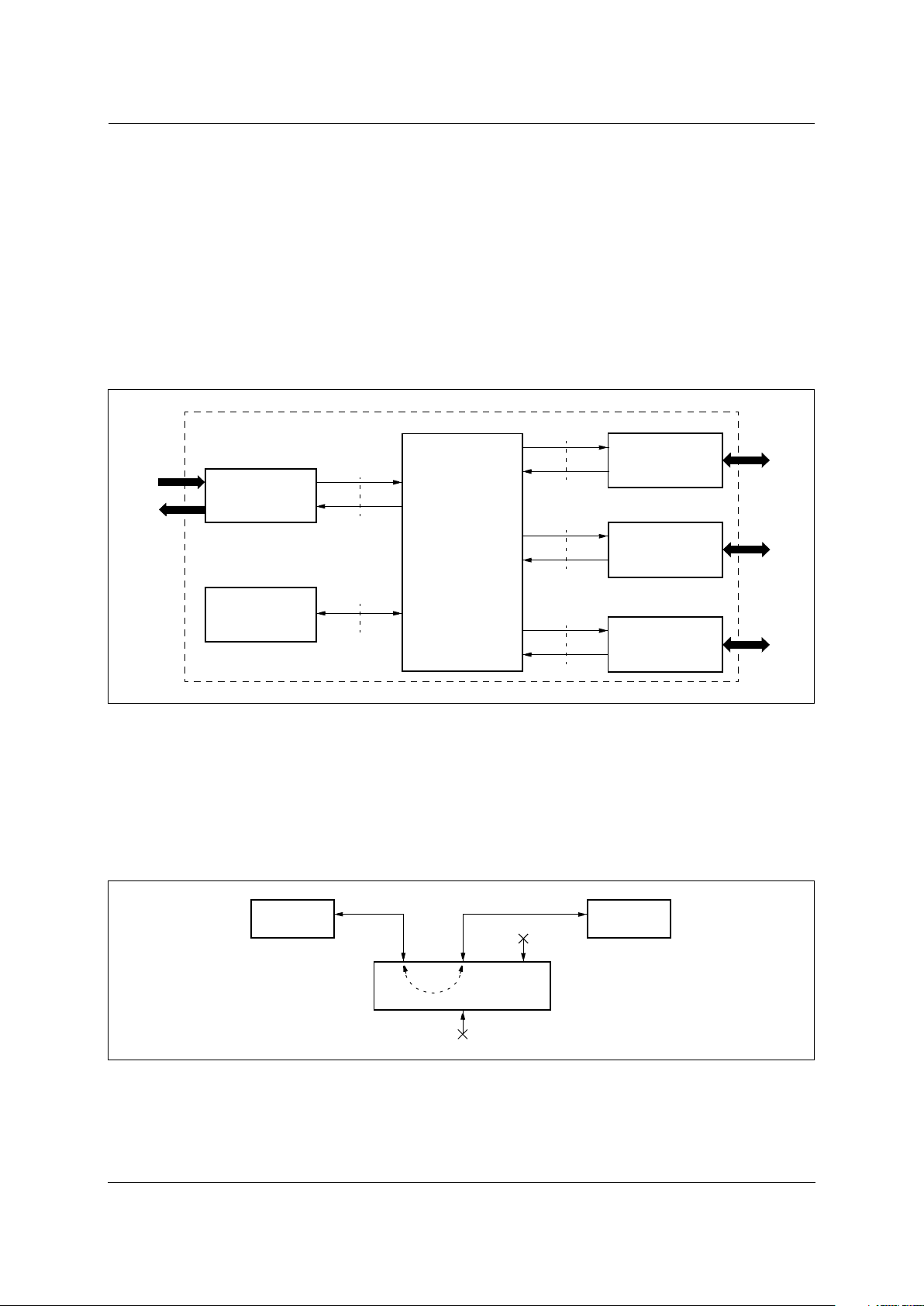
1.1.1 Repeaters
Figure 1-2 shows single pair repeaters placed in line between HDSL terminals to
extend transmission distance. RS8953B provides an internal cross-connect path
between HDSL channels 1 and 2 to support single pair repeaters.
Figure 1-1. HTU Block Diagram
PCM Channel
MPU Bus
HDSL
Channel 1
HDSL
Channel 2
HDSL
Channel 3
RS8953B
HDSL
Channel Unit
T1/E1
Transceiver
MPU
ZipWire Transceiver
ZipWire Transceiver
ZipWire Transceiver
CH1
CH2
CH3
Figure 1-2. Repeater System Block Diagram
RS8953B
PCM
CH1
CH2
CH3
Page 17

RS8953B/RS8953SPB
1.0 HDSL Systems
HDSL Channel Unit
1.1 HTU Applications
N8953BDSB Conexant 1-3
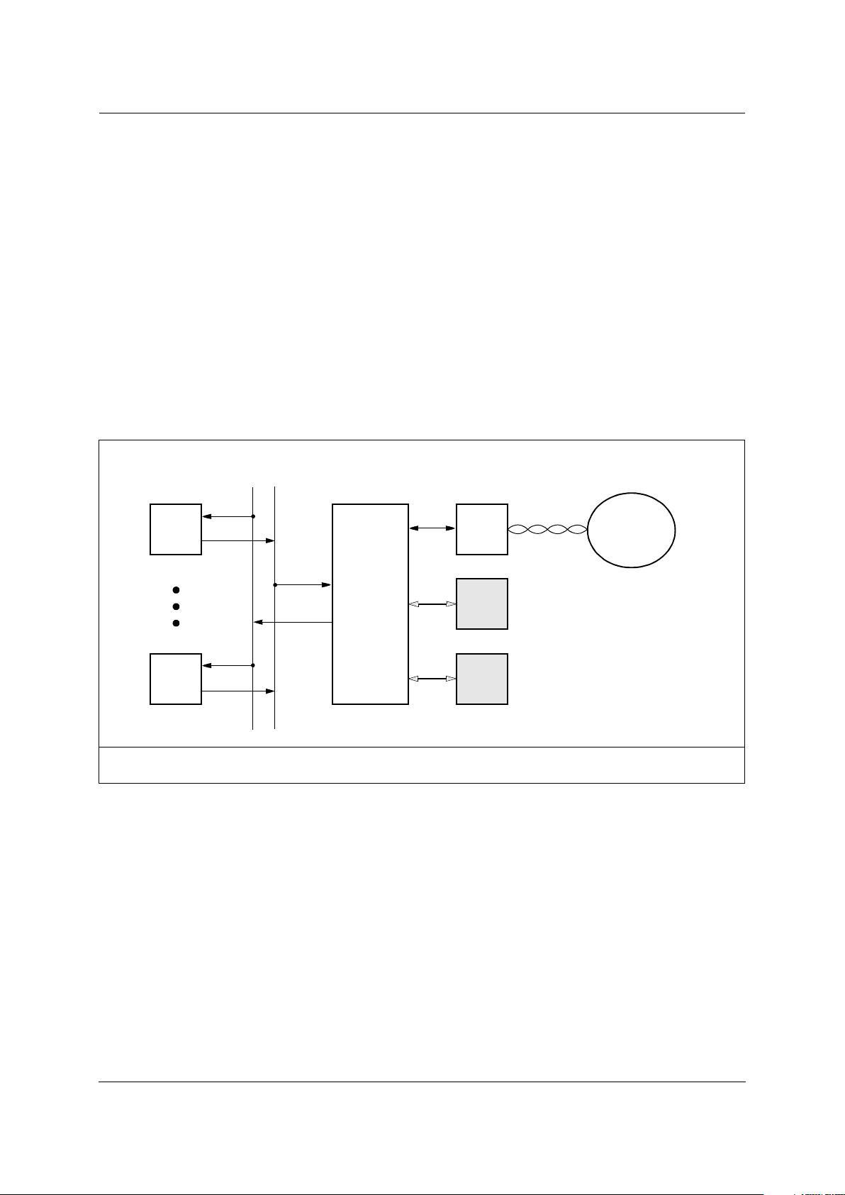
1.1.2 Fractional Transport
Figure 1-3 illustrates a drop/insert application where only a portion of the PCM
channel bandwidth is transported over one or more HDSL wire pairs. The
RS8953B provides drop/insert indicator signals to control external data MUXes
and internal routing tables to map timeslots from either one of two synchronized
PCM data sources. For remote terminals using partial payloads, the PCM channel
may be configured to operate either at the standard interface rate or at the Nx64
effective payload rate.
Figure 1-3. Drop/Insert System Block Diagram
Mux
HDSL
CH1
HDSL
CH2
HDSL
CH3
PCMD/I
Optional
RS8953B HDSL Channel Unit
Transceiver
Drop
Insert
T1/E1
FIBER
or Other
Transceiver
T1/E1
FIBER
or Other
Mux
Page 18

1.0 HDSL Systems
RS8953B/RS8953SPB
1.1 HTU Applications
HDSL Channel Unit
1-4 Conexant N8953BDSB
1.1.3 Switching Systems
Figure 1-4 illustrates how the RS8953B is incorporated into a digital switch or
multiplexer system that uses multiple HDSL lines to transport Nx64 or standard
T1/E1 applications. The RS8953B’s PCM timeslot router contains 64 table entries
that extends the maximum PCM channel rate to 64x64 or 4.096 Mbps. RS8953B
allows PCM channels at the central office (CO) and remote ends to operate at
different rates. For example, the PCM channel in a digital switch may connect to a
4.096 Mbps shelf bus, while the remote terminal connects to a T1/E1 standard
PCM channel.
Figure 1-4. Switch/Mux System Block Diagram
NOTE(S):
SLIP BUFFER = Optional frame SLIP BUFFER to align receive PCM with local master frame.
DS0 Switch Matrix
RS8953B RS8953B
CH1 CH2 CH3 CH1 CH2 CH3
Nx64 Nx64
SLIP
BUFFER
SLIP
BUFFER
Page 19
RS8953B/RS8953SPB
1.0 HDSL Systems
HDSL Channel Unit
1.1 HTU Applications
N8953BDSB Conexant 1-5
1.1.4 Loop Carrier/Pair Gain
Figure 1-5 shows a channel bank application where the PCM channel connects a
bank of voice and/or data subscriber line interfaces using an Nx64 bus. The total
number of subscriber lines determines the PCM channel rate and determines how
many HDSL wire pairs are needed to transport the application up to the digital
loop carrier, cellular base station, network distribution element, or to the private
branch exchange. The RS8953B supplies the PCM frame sync reference and acts
as the PCM bus master for the remote channel bank. The RS8953B’s Digital
Phase Locked Loop (DPLL) clock recovery allows PCM channel rates down to
2x64 or 128 kpbs. Unpopulated PCM timeslots or HDSL payload bytes can be
replaced by an 8-bit programmable fixed pattern, or one of four Pseudo-Random
Bit Sequence (PRBS) patterns.
Figure 1-5. Voice (Pairgain/Cellular/PCS) System Block Diagram
NOTE(S):
SLI = Subscriber Line Interface
Loop, Access,
or Distribution
Node
CH1
CH2
CH3
RS8953B
SLI
1
SLI
n
Nx64
Bus
Optional
Page 20
1.0 HDSL Systems
RS8953B/RS8953SPB
1.1 HTU Applications
HDSL Channel Unit
1-6 Conexant N8953BDSB
1.1.5 Point-to-Multipoint
Figure 1-6 shows fractional T1/E1 services delivered from the CO to multiple
remote sites in a Point-to-Multipoint (P2MP) application. The number of HDSL
wire pairs and PCM channel rates at each site is variable. The RS8953B provides
the ability to measure and compensate for misalignment between separate PCM
frame syncs coming from each remote site. By programming transmit delays from
PCM to HDSL frame syncs, each remote site can send its HDSL frames back to
the central office. The HDSL frames are then sufficiently aligned with the others
to be reconstructed into a single PCM frame at the central site. The RS8953B
accommodates large differential delays associated with the P2MP application. It
receives HDSL frame offsets to groom Channel Associated Signaling (CAS)
from different sites.
P2MP applications of primary rate ISDN transport are also supported, where
different LAPD channels are received from each remote site. The RS8953B
provides auxiliary HDSL channel inputs and outputs for the system to externally
insert and monitor transmitted or received HDSL payload bytes. Auxiliary HDSL
channels may alternately be configured to terminate the last 40 Z-bits through an
external data link controller.
Figure 1-6. Point-to-Multipoint (Fractional) System Block Diagram
NOTE(S):
1. SCC = Serial Communications Controller
2. LAPD = Link Access Procedure D-Channel
3. AUX = Auxiliary HDSL channel attaches to payload or Z-bits
RS8953B
Full
T1/E1
RS8953B
CH1
CH2
CH3
CH1
Partial
T1/E1
Site C
RS8953B
CH1
Partial
T1/E1
Site B
RS8953B
CH1
Partial
T1/E1
Site A
SCC SCC SCC
Aux1
Aux2
Aux3
Optional
Management Protocol
LAPD Signaling or
Page 21
RS8953B/RS8953SPB
1.0 HDSL Systems
HDSL Channel Unit
1.1 HTU Applications
N8953BDSB Conexant 1-7
1.1.6 Subscriber Modem
Figure 1-7 shows an HDSL data modem application where a CPU processor
delivers PCM data directly to the RS8953B. Alternately, a multichannel
communications controller such as the Bt8071A can be used to manage the
transfer of data between the CPU and PCM channel through a local shared
memory.
Figure 1-7. Subscriber Modem (Terminal) System Block Diagram
Single Channel Payload
RS8953B
CH1
CH2
CH3
CPU
Memory
Serial
Port
Optional
RS8953B
CH1
CH2
CH3
PCM
Bt8071A
32-Channel
HDLC Controller
CPU
Shared
Multichannel Payload
Optional
Memory
Page 22
1.0 HDSL Systems
RS8953B/RS8953SPB
1.2 System Interfaces
HDSL Channel Unit
1-8 Conexant N8953BDSB
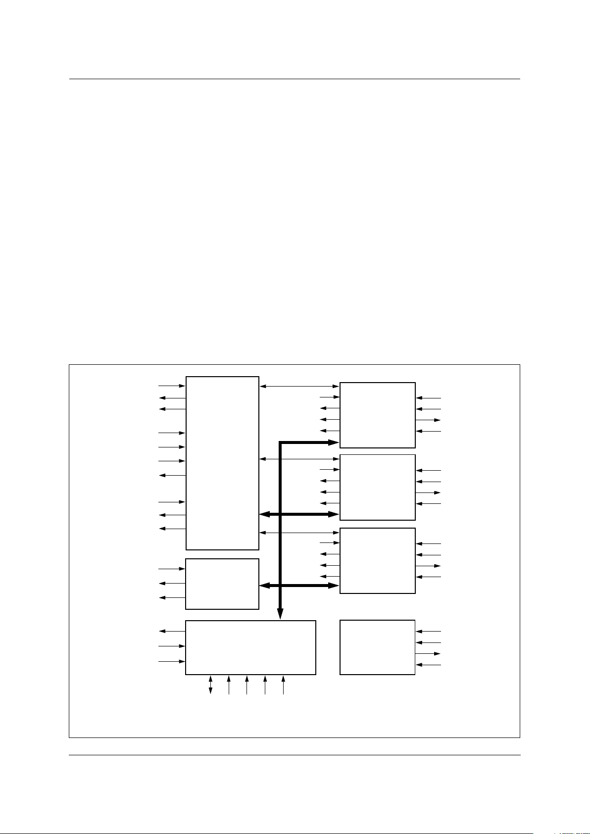
1.2 System Interfaces
System interfaces and associated signals for the RS8953B functional circuit
blocks are shown in Figure 1-8. Circuit blocks are described in sections 3 and 4,
and signals are defined in Ta bl e 2- 2 .
The single-pair version (RS8953SPBEPF and RS8953SPBEPJ) only supports
HDSL Channel 1. HDSL Channels 2 and 3 are not usable. Although only 1 HDSL
channel is usable, the internal registers are not changed from the 3 HDSL channel
versions. The single-pair versions (RS8953SPBEPF and RS8953SPBEPJ) only
supports HDSL Channel 1. HDSL Channels 2 and 3 are not usable. Although
only 1 HDSL channel is usable, the internal registers are not changed from the 3
HDSL channel versions. This means that the registers should be programmed
with the same value as if only HDSL channel 1 was used in a 3 channel version.
This allows the 3 channel version to be used for development, and without a
software change, a single-pair version used for production.
Figure 1-8. RS8953B System Interfaces
MCLK
RCLK
INSDAT
INSERT
DROP
EXCLK
TCLK
TSER
TMSYNC
MSYNC
RSER
RMSYNC
SCLK
INTR*
RST*
MPUSEL
TAUX1
TLOAD1
RAUX1
ROH1
TAUX2
TLOAD2
RAUX2
ROH2
TAUX3
TLOAD3
RAUX3
ROH3
BCLK1
QCLK1
TDAT1
RDAT1
BCLK2
QCLK2
TDAT2
RDAT2
BCLK3
QCLK3
TDAT3
RDAT3
AD[7:0]
CS*
ALE
RD*
WR*
PCM
Channel
HDSL
Channel1
HDSL
Channel2
HDSL
Channel3
MPU
Interface
DPLL
TCK
TDI
TDO
TMS
Tes t
Access
Page 23

N8953BDSB Conexant 2-1
2
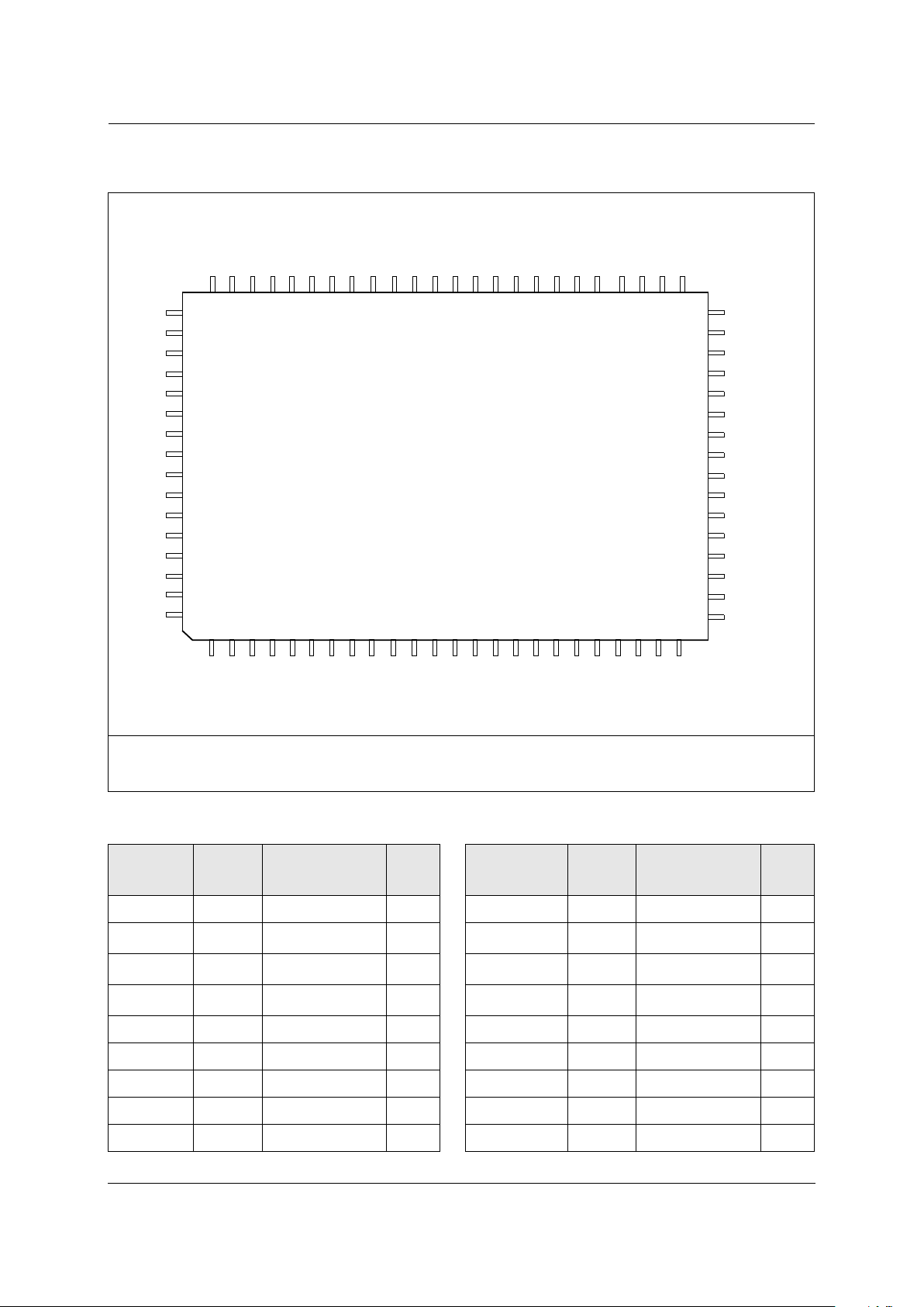
2.0 Pin Descriptions
2.1 Pin Assignments
The RS8953B pin assignments for the 68–pin Plastic Leaded Chip Carrier
(PLCC) package are shown in Figure 2-1 and Figure 2-2. The RS8953B pin
assignments for the 80–pin Plastic Quad Flat Pack (PQFP) are shown in
Figure 2-3 and Figure 2-4. The pinouts for RS8953B packages are listed in
Table 2- 1 and defined in Ta bl e 2- 2. The input/output (I/O) column in Tab le 2 -1 is
coded as follows:
I = Input, O = Output, I/O = Bidirectional, VCC = Power, GND = Ground, and
NC = No Connection.
Page 24
2.0 Pin Descriptions
RS8953B/8953SPB
2.1 Pin Assignments
HDSL Channel Unit
2-2 Conexant N8953BDSB
Figure 2-1. Three-Pair PLCC Pin Assignments
TDAT3
SCLK
MSYNC/RAUX3
TAUX3
TAUX2
TAUX1
TLOAD3
TLOAD2
TLOAD1
WR*
ALE
VCC
PLLVCC
PLLDGND
PLLAGND
VEXT
VCC
RDAT1
AD[0]
AD[1]
AD[2]
AD[3]
AD[4]
AD[5]
AD[6]
AD[7]
VCC
EXCLK
INSDAT
INSERT/RAUX2
INTR*
TMSYNC
RMSYNC
GND
VCC
ROH3
RDAT3
BCLK3
GND
QCLK3
ROH2
QCLK2
GND
BCLK2
TDAT2
RDAT2
GND
BCLK1
ROH1
TDAT1
QCLK1
VCC
MCLK
CS*
DROP/RAUX1
GND
TMS
TDO
TDI
TCK
RST*
RD*
RSER
TSER
RCLK
TCLK
MPUSEL
VCC
60
59
58
57
56
55
54
53
52
51
50
49
48
47
46
45
44
10
11
12
13
14
15
16
17
18
19
20
21
22
23
24
25
26
61
62
63
64
65
66
67
68
1
2
3
4
5
6
7
8
9
43
42
41
40
39
38
37
36
35
34
33
32
31
30
29
28
27
RS8953BEPJ
Page 25
RS8953B/8953SPB
2.0 Pin Descriptions
HDSL Channel Unit
2.1 Pin Assignments
N8953BDSB Conexant 2-3
Figure 2-2. Single-Pair PLCC Pin Assignments
NOTE(S):
(1)
These pins are only functional when RAUX_EN is not active (RAUX_EN = 0).
NC
SCLK
MSYNC
(1)
NC
NC
TAUX1
NC
NC
TLOAD1
WR*
ALE
VCC
PLLVCC
PLLDGND
PLLAGND
VEXT
VCC
RDAT1
AD[0]
AD[1]
AD[2]
AD[3]
AD[4]
AD[5]
AD[6]
AD[7]
VCC
EXCLK
INSDAT
INSERT
(1)
INTR*
TMSYNC
RMSYNC
GND
VCC
NC
NC
NC
GND
NC
NC
NC
GND
NC
NC
NC
GND
BCLK1
ROH1
TDAT1
QCLK1
VCC
MCLK
CS*
DROP/RAUX1
GND
TMS
TDO
TDI
TCK
RST*
RD*
RSER
TSER
RCLK
TCLK
MPUSEL
VCC
60
59
58
57
56
55
54
53
52
51
50
49
48
47
46
45
44
10
11
12
13
14
15
16
17
18
19
20
21
22
23
24
25
26
61
62
63
64
65
66
67
68
1
2
3
4
5
6
7
8
9
43
42
41
40
39
38
37
36
35
34
33
32
31
30
29
28
27
RS8953SPBEPJ
Page 26

2.0 Pin Descriptions
RS8953B/8953SPB
2.1 Pin Assignments
HDSL Channel Unit
2-4 Conexant N8953BDSB
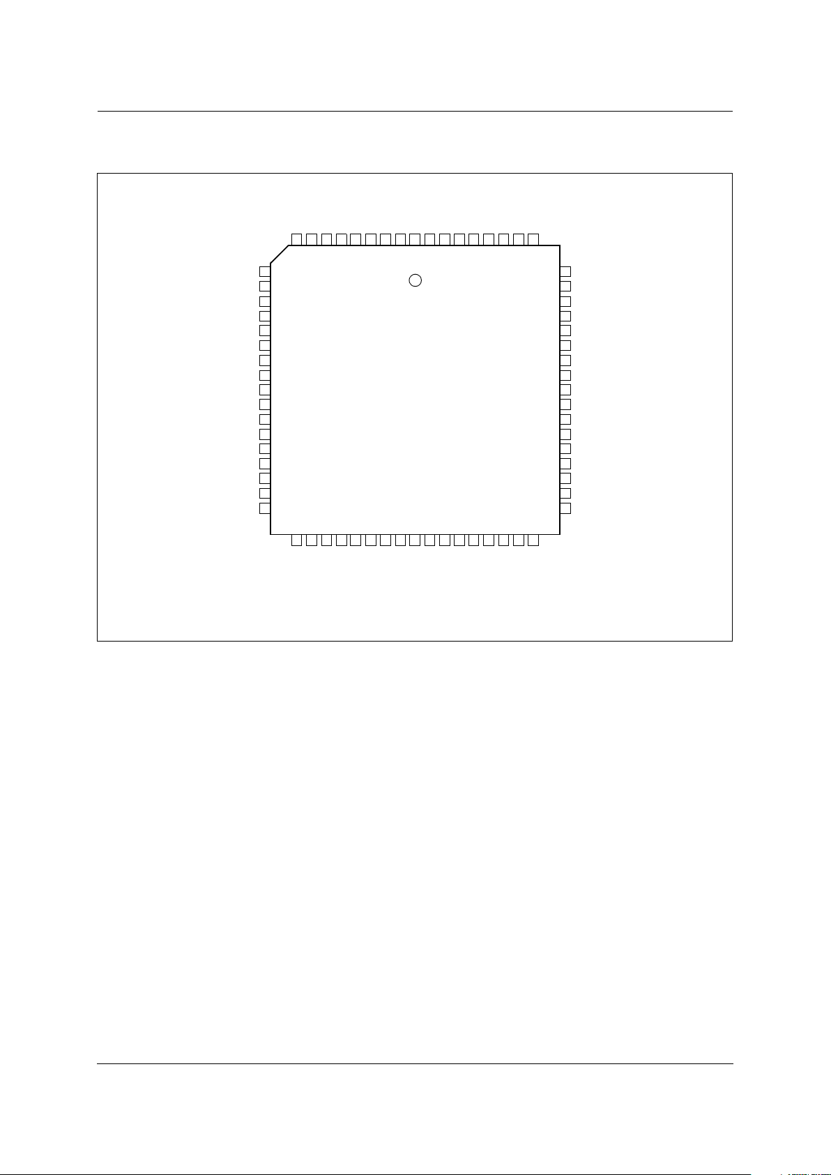
Figure 2-3. Three-Pair PQFP Pin Assignments
59 58 57 56 55 54 53 52 51 50 49 48 47 46 45 44 43 42 4161626364
65
66
67
68
69
70
71
72
73
74
75
76
77
78
21 3 4 5 6 7 8 9 1011121314151617181920
40
39
38
37
36
35
34
33
32
31
30
29
28
27
26
25
24232221
MCLK
CS*
NC
MPUSEL
BCLK2
NC
TDAT2
RDAT2
GND
BCLK1
QCLK1
NC
AD[0]
AD[1]
AD[2]
AD[3]
AD[4]
AD[5]
AD[6]
AD[7]
VCC
NC
EXCLK
INSDAT
INSERT/RAUX2
INTR*
TMSYNC
RMSYNC
RS8953BEPF
60
79
80
ROH1
TDAT1
NC
RDAT1
GND
GND
VCC
NCNCVCC
VCC
SCLK
ROH3
VCC
NC
TDAT3
NC
VEXT
PLLAGND
PLLDGND
PLLVCC
VCC
ALE
WR*
TLOAD1
TLOAD2
TLOAD3
TAUX1
TAUX2
TAUX3
MSYNC/RAUX3
DROP/RAUX1
GND
TMS
NC
TD0
TDI
TCK
RST*
RD*
RSER
TSER
RCLK
TCLK
RDAT3
BCLK3
GND
QCLK3
ROH2
QCLK2
GND
GND
Page 27
RS8953B/8953SPB
2.0 Pin Descriptions
HDSL Channel Unit
2.1 Pin Assignments
N8953BDSB Conexant 2-5
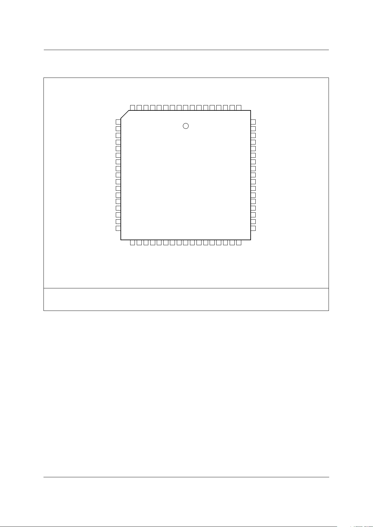
Figure 2-4. Single-Pair PQFP Pin Assignments
NOTE(S):
(1)
These pins are only functional when RAUX_EN is not active (RAUX_EN = 0).
59 58 57 56 55 54 53 52 51 50 49 48 47 46 45 44 43 42 41
NC
NC
NC
VCC
61626364
65
66
67
68
69
70
71
72
73
74
75
76
77
78
21 3 4 5 6 7 8 9 1011121314151617181920
40
39
38
37
36
35
34
33
32
31
30
29
28
27
26
25
24232221
VCC
TAUX1
NC
NC
MSYNC
(1)
SCLK
MCLK
CS*
NC
DROP/RAUX1
GND
TMS
NC
TDO
TDI
TCK
RST*
RD*
RSER
TSER
RCLK
TCLK
MPUSEL
NC
NC
GND
NC
NC
NC
GND
GND
NC
NC
NC
NC
GND
BCLK1
QCLK1
NC
AD[0]
AD[1]
AD[2]
AD[3]
AD[4]
AD[5]
AD[6]
AD[7]
VCC
NC
EXCLK
INSDAT
INSERT
(1)
INTR*
TMSYNC
RMSYNC
RS8953SPBEPF
60
79
80
ROH1
TDAT1
NC
RDAT1
GND
GND
VCC
NC
VCC
NC
NC
NC
VEXT
PLLAGND
PLLDGND
PLLVCC
VCC
ALE
WR*
TLOAD1
NC
Table 2-1. Pin Assignments (1 of 2)
80-Pin
PQFP
68-Pin
PLCC
Signal I/O 80-Pin PQFP
68-Pin
PLCC
Signal I/O
71, 72 1 GND GND 33 37 TDO O
73 2
BCLK2
(1)
I3538TMSI
75 3
TDAT2
(1)
O3639GNDGND
76 4
RDAT2
(1)
I 37 40 DROP/RAUX1 O
77 5 GND GND 39 41 CS* I
78 6 BCLK1 I 40 42 MCLK I
79 7 ROH1 O 41 43 VCC VCC
80 8 TDAT1 O 43 44 VCC VCC
1 9 QCLK1 I 45 45 VEXT I
Page 28

2.0 Pin Descriptions
RS8953B/8953SPB
2.1 Pin Assignments
HDSL Channel Unit
2-6 Conexant N8953BDSB
3 10 RDAT1 I 32 36 TDI I
5 11 AD[0] I/O 46 46 PLLAGND GND
6 12 AD[1] I/O 47 47 PLLDGND GND
7 13 AD[2] I/O 48 48 PLLVCC VCC
8 14 AD[3] I/O 49 49 VCC(SCAN_MD) VCC
9 15 AD[4] I/O 50 50 ALE I
10 16 AD[5] I/O 51 51 WR* I
11 17 AD[6] I/O 52 52 TLOAD1 O
12 18 AD[7] I/O 53 53
TLOAD2
(1)
O
13 19 VCC VCC 54 54
TLOAD3
(1)
O
15 20 EXCLK I 55 55 TAUX1 I
16 21 INSDAT I 56 56
TAUX2
(1)
I
17 22
INSERT/RAUX2
(2)
O5757
TAUX3
(1)
I
18 23 INTR* O 58 58
MSYNC/RAUX3
(2)
O
19 24 TMSYNC I 59 59 SCLK O
20 25 RMSYNC O 60 60
TDAT3
(1)
O
21, 22 26 GND GND 63 61 VCC VCC
23 27 VCC VCC 64 62
ROH3
(1)
O
24 28 MPUSEL I 65 63
RDAT3
(1)
I
25 29 TCLK I 66 64
BCLK3
(1)
I
26 30 RCLK O 67 65 GND(SCAN_EN) GND
27 31 TSER I 68 66
QCLK3
(1)
I
28 32 RSER O 69 67
ROH2
(1)
O
29 33 RD* I 70 68
QCLK2
(1)
I
30 34 RST* I 2, 4, 14, 34,
38, 42, 44, 61,
62, 74
—NC—
31 35 TCK I — —
—
—
NOTE(S):
(1)
These pins do not perform the functions in RS8953SPBEPF and RS8953SPBEPJ.
(2)
These pins are only functional in RS8953SPBEPF and RS8953SPBEPJ when RAUX_EN is not active (RAUX_EN = 0).
Table 2-1. Pin Assignments (2 of 2)
80-Pin
PQFP
68-Pin
PLCC
Signal I/O 80-Pin PQFP
68-Pin
PLCC
Signal I/O
Page 29

RS8953B/8953SPB
2.0 Pin Descriptions
HDSL Channel Unit
2.2 Signal Definitions
N8953BDSB Conexant 2-7
2.2 Signal Definitions
Table 2-2. Signal Definitions (1 of 4)
Signal Name I/O Description
Microprocessor (MPU) Interface
MPUSEL MPU Select
I
(1)
Determines the type of MPU bus control signals expected during data transfers.
Intel (MPUSEL = 0) or Motorola (MPUSEL = 1) bus types are supported. RD*
and WR* signal functions are affected.
AD[0:7] Address/Data Bus
I/O
(1)
Eight multiplexed address and data signals. The address is latched on the falling
edge of ALE and selects one of 256 internal register locations (0x00-0xFF). The
data bus transfers the contents of the latched address location during the read
or write cycle.
CS* Chip Select
I
(1)
Active-low input enables MPU read and write cycles. The rising edge of CS*
completes the read or write data transfer cycle and places the address/data bus
(AD[0]–AD[7]) in a high impedance state.
ALE Address Latch
Enable
I
(1)
Active-high input enables the address bus. The falling edge of ALE latches the
address internally.
RD* Read Strobe
I
(1)
Signal function determined by MPUSEL:
MPUSEL = 0; RD* is an active low data strobe for read cycles.
MPUSEL = 1; RD* is an active low data strobe for read/write cycles.
WR* Write Strobe
I
(1)
Signal function determined by MPUSEL:
MPUSEL = 0; WR* is an active low data strobe for write cycles.
MPUSEL = 1; WR* controls the data bus transfer direction: high during read
cycles and low during write cycles.
INTR* Interrupt Request O Active low, open-drain output indicates when any one or more Interrupt Request
Register (IRR) bit is high and its respective Interrupt Mask Register (IMR) bit is
low. INTR* remains active until all pending interrupts are cleared by writing 0s
to their corresponding Interrupt Clear Register (ICR) bits.
RST* Reset
I
(1)
Active low input required to initialize internal circuits after power and master
clock have been applied. All MPU registers remain accessible while reset is
active. Unless stated otherwise, reset activation does not affect the MPU register
contents.
RS8953B reset activation disables interrupts on the INTR* output by forcing
all 1s in the Interrupt Mask Register (IMR), and zeros in the TX_ERR_EN,
DPLL_ERR_EN, and RX_ERR_EN bits.
RS8953B reset activation disables auxiliary channels by forcing zeros in all
TAUX_EN and RAUX_EN bits.
To facilitate system upgrades from prototype Bt8953EPF, RS8953B reset
activation also forces zeros in those command register bits which do not exist
on Bt8953EPF, but were added on RS8953B.
Page 30

2.0 Pin Descriptions
RS8953B/8953SPB
2.2 Signal Definitions
HDSL Channel Unit
2-8 Conexant N8953BDSB
HDSL Channels
BCLK1 Bit Clock
I
(1)
Corresponds to three HDSL and three Auxiliary channels. BCLKn operates at
twice the 2B1Q symbol rate. The rising edge of BCLKn outputs TDATn, TLOADn,
RAUXn and ROHn; the falling edge samples QCLKn, RDATn, and TAUXn inputs.
BCLK2
(3)
BCLK3
(3)
QCLK1 Quaternary Clock
I
(1)
Operates at the 2B1Q symbol rate (half-bit rate) and identifies sign and
magnitude alignment of both RDATn and TDATn serially encoded bit streams.
The falling edge of BCLKn samples QCLKn: 0 = sign bit; 1 = magnitude bit.
QCLK2
(3)
QCLK3
(3)
TDAT1 Transmit Data O HDSL transmit data output at the bit rate on the rising edge of BCLKn. Serially
encoded with the 2B1Q sign bit aligned to the QCLKn low level and the 2B1Q
magnitude bit aligned to the QCLKn high level.
TDAT2
(3)
TDAT3
(3)
TAUX1 Transmit
Auxiliary Data
I
(1)
HDSL transmit auxiliary data input sampled on the falling edge of BCLKn when
TLOADn is active. TAUXn replaces data normally supplied by PCM or HDSL
transmitters to the HDSL scrambler input. Payload bytes or Z-bits can be
mapped from TAUXn.
TAU X2
(3)
TAU X3
(3)
RDAT1 Receive Data
I
(1)
HDSL receive data input sampled on the falling edge of BCLKn. The serially
encoded 2B1Q sign bit is sampled when QCLKn is low, and the 2B1Q magnitude
bit is sampled when QCLKn is high.
RDAT2
(3)
RDAT3
(3)
RAUX1 Receive Auxiliary
Data
O Receives data from the HDSL descrambler output on the rising edge of BCLKn.
Includes all SYNC, STUFF, HOH, payload, and Z-bits. RAUXn shares pin locations
with DROP, INSERT, and MSYNC, as controlled by RAUX_EN (CMD_6; addr
0xF3).
RAUX2
(3)
RAUX3
(3)
TLOAD1 Transmit Load
Indicator
O Active-high output that indicates when specific payload or Z-bits are sampled at
TAUXn. TLOADn is active for 8 bits coincident with each marked payload byte or
1 bit for Z-bits. The last 40 Z-bits or any combination of payload bytes may be
marked.
TLOAD2
(3)
TLOAD3
(3)
ROH1 Receive Overhead
Indicator
O Indicate when overhead is received. Has two modes of operation:
• RAS = 0. ROHn is high to mark only data passed into the RFIFO.
• RAS=1. ROHn is high to mark only the last 40 Z-bits.
ROH2
(3)
ROH3
(3)
Table 2-2. Signal Definitions (2 of 4)
Signal Name I/O Description
Page 31

RS8953B/8953SPB
2.0 Pin Descriptions
HDSL Channel Unit
2.2 Signal Definitions
N8953BDSB Conexant 2-9
PCM Channel
TCLK Transmit Clock
I
(2)
Operates at the PCM bit rate and samples the PCM transmit inputs: TSER,
TMSYNC, and INSDAT; and clocks the PCM transmit output, INSERT. Falling
edge samples and rising edge outputs are normal, inverted TCLK edges are
selectable. Optionally, RCLK or EXCLK can be programmed as the PCM transmit
clock for loopback or externally timed applications.
RCLK Receive Clock O Operates at the PCM bit rate and clocks the PCM receive outputs: RSER,
RMSYNC, and DROP. Normally, RCLK is supplied by the internal clock recovery
DPLL. Optionally, EXCLK or TCLK can be programmed as the receive source
during loopback or externally timed applications. Rising-edge (normal) or
falling-edge (inverted) output transitions are selectable.
EXCLK External Clock
I
(2)
Optionally sources the PCM Receive Clock (RCLK), or both RCLK and PCM
Transmit Clock (TCLK) for systems that supply a local master clock. Normal or
inverted edges are also selectable.
TSER Transmit Serial
Data
I
(1)
Accepts up to 64 timeslots (1 timeslot = 8 bits) of data and an optional framing
bit per PCM frame. TSER data and F-bits are then routed and mapped into the
HDSL transmit channel payload.
RSER Receive Serial
Data
O Outputs up to 64 timeslots of data and an optional F-bit per PCM frame. Receive
serial data and F-bits are constructed by mapping and combining payload from
the HDSL receive channels.
TMSYNC Transmit
Multiframe Sync
I
(1)
Active-high input resets the PCM transmit time base during framed applications.
TMSYNC is ignored in unframed or asynchronously mapped applications. The
low to high input state transition is detected and internally delayed by a
programmable bit and frame offset to coincide with the TSER and INSDAT
sample location of bit 0, frame 0. The programmable sample point
accommodates any system’s rising edge frame or multiframe sync signal.
RMSYNC Receive
Multiframe Sync
O Active-high output from the receive timebase, typically programmed to mark
PCM multiframe boundaries during framed applications, and remains unused
during unframed or asynchronously mapped applications. RMSYNC pulses high
for one RCLK coincident with RSER output of bit 0, frame 0. Bit 0 is the first bit
in TS0 of an E1 or Nx64 frame, or the F-bit of a T1 frame. Programmable bit and
frame delays allow RMSYNC to mark any desired RSER bit.
MSYNC Transmit Master
Sync
O Active-high output pulses high for one TCLK to mark two clock cycles before the
TSER and INSDAT sample point of bit 0, frame 0, of a transmit multiframe.
MSYNC references the TMSYNC applied by the system or supplies the system
with a master PCM frame/multiframe sync signal.
Table 2-2. Signal Definitions (3 of 4)
Signal Name I/O Description
Page 32

2.0 Pin Descriptions
RS8953B/8953SPB
2.2 Signal Definitions
HDSL Channel Unit
2-10 Conexant N8953BDSB
Drop/Insert
DROP Drop Indicator O Active-high output indicates when specific PCM timeslots are present on RSER.
DROP is high for 8 bits coincident with each marked timeslot, or 1 bit when
marking F-bits. Any combination of timeslots and F-bits within the PCM frame
can be marked.
INSDAT Insert Data
I
(1)
Alternate source of PCM transmit serial data. INSDAT is sampled by TCLK and
replaces TSER when INSERT is active. INSDAT and TSER use the same frame
format. INSDAT can be programmed to replace TSER data on a
per-timeslot-basis.
INSERT Insert Indicator O Active-high output indicates when specific INSDAT timeslots are sampled.
INSERT is high for 8 bits coincident with each marked timeslot or for 1 bit when
marking F-bits. Any combination of timeslots and F-bits within the PCM frame
can be marked.
DPLL and Power
MCLK Master Clock I Runs through a multiplier PLL to create an internal 60–80 MHz reference clock
for the DPLL. The 16 times symbol rate clock from a Conexant HDSL transceiver
typically connects to MCLK. However, MCLK is not required to be synchronized
to any HDSL or PCM channel. The DPLL reference clock is used to synthesize
the PCM Recovered Clock (RCLK) based on DPLL programmed values.
Optionally, a 60–80 MHz clock can be input directly on MCLK.
SCLK System Clock O The internal 60–80 MHz DPLL reference clock is divided by 4 to create a
15–20 MHz system clock output on SCLK. SCLK can be applied to other devices
requiring a system clock (i.e., Bt8360 or Bt8510).
VEXT External Voltage I Used to bias input protection diodes. If interfacing to 5 V powered devices,
connect this pin to 5 V. Otherwise, connect 3.3 V to this pin.
PLLVCC PLL Power I 3.3 Vdc +/– 0.3 V power input for the PLL.
PLLDGND PLL Ground I 0 Vdc ground reference for the PLL.
PLLAGND PLL Analog
Ground
I 0 Vdc analog ground reference for the PLL. Tied to GND unless PLL operation is
desired above 80 MHz.
VCC Power I 3.3 Vdc +/– 0.3 V power input.
GND Ground I 0 Vdc ground reference.
TCK Test Clock I Boundary scan clock samples and outputs test access signals.
TMS Test Mode Select
I
(1)
Active-high enables test access port. Sampled by TCK rising edge.
TDI Test Data Input
I
(1)
Serial data for boundary scan chain. Sampled by TCK rising edge.
TDO Test Data Output O Outputs serial data from boundary scan chain on TCK falling edge.
NOTE(S):
(1)
Internal pull-ups (80-100 kW) are present on inputs to allow unused inputs to remain disconnected.
(2)
Internal pull-downs (80-100 kW) are present on inputs to allow unused inputs to remain disconnected.
(3)
The pins do not perform these functions in RS8953SPBEPF and RS8953SPBEPJ.
Table 2-2. Signal Definitions (4 of 4)
Signal Name I/O Description
Page 33

N8953BDSB Conexant 3-1
3
3.0 Circuit Descriptions
3.1 MPU Interface
The Microprocessor Unit (MPU) interface consists of an 8-bit parallel
multiplexed address-data bus, an associated bus control signal, and a maskable
interrupt request output, as illustrated in Figure 3-1 and Figure 3-2. The MPU
interface is compatible with 8-bit processors running at bus cycle speeds up to
16 MHz. Systems that use 16 or 32-bit processors can add an external address
buffer and data transceiver to connect the RS8953B. Faster bus speeds require
external wait-state insertion logic.
Figure 3-1. MPU Bus Control Logic
MPUSEL
RD*
WR*
Read Strobe
Write Strobe
CS*
ALE
AD[7:0]
To Registers
From Registers
Address
Page 34

3.0 Circuit Descriptions
RS8953B/8953SPB
3.1 MPU Interface
HDSL Channel Unit
3-2 Conexant N8953BDSB
3.1.1 Address/Data Bus
Address/data bus pins AD[7:0] allow MPU access to RS8953B internal registers.
Read and write access is allowed at any of the 256 address locations, but only
defined register address locations are applicable (see Tab le 4 -1 ).
3.1.2 Bus Controls
Five signals control register access: ALE, CS*, RD*, WR*, and MPUSEL. The
address on AD[7:0] is latched on the falling edge of ALE, and CS* is an
active-low port enable for all read and write operations. If CS* is high, the MPU
port is inactive.
Different styles of bus control are supported using separate read and write
strobes for Intel-style buses, or common data strobe with a combined read/write
signal for Motorola-style buses. When MPUSEL = 0 (Intel bus), RD* is an
active-low read enable and WR* is an active-low write strobe. While RD* and
CS* are low, the addressed register’s data is driven onto AD[7:0]. If WR* and
CS* are low, the rising edge of WR* or CS* latches data from AD[7:0] into the
register. When MPUSEL = 1 (Motorola bus), RD* is an active-low data strobe for
both read and write cycles, and WR* is a read/write select. While RD* and CS*
are low and WR* is high, the addressed register’s data is driven onto AD[7:0]. If
RD*, CS*, and WR* are low, the rising edge of RD*, CS*, or WR* latches data
from AD[7:0].
Figure 3-2. MPU Interrupt Logic
Interrupt
DATA
INTR*
Mask
Request
Set
Write ICR
Write IMR
Other Interrupt
Sources
Read IMR
Read IRR
Reset
Event
Page 35

RS8953B/8953SPB
3.0 Circuit Descriptions
HDSL Channel Unit
3.1 MPU Interface
N8953BDSB Conexant 3-3
3.1.3 Interrupt Request
The open-drain interrupt request output (INTR*) indicates when a particular set
of transmit, receive, or common status registers have been updated. Eight
maskable interrupt sources are requested on the common INTR* pin:
1.
TX1 = Channel 1 Transmit 6 ms Frame
2.
TX2 = Channel 2 Transmit 6 ms Frame
3.
TX3 = Channel 3 Transmit 6 ms Frame
4.
RX1 = Channel 1 Receive 6 ms Frame
5.
RX2 = Channel 2 Receive 6 ms Frame
6.
RX3 = Channel 3 Receive 6 ms Frame
7.
TX_ERR = Logical OR of 3 Transmit Channel Errors
8.
RX_ERR = Logical OR of 3 Receive Channel Errors and DPLL Errors
All interrupt events are edge-sensitive and synchronized to their respective
HDSL channel’s 6 ms frame. The basic structure of each interrupt source is
shown in Figure 3-2, with three associated registers: Interrupt Mask Register
[IMR; addr 0xEB], where writing a 1 to an IMR bit prevents the associated
interrupt source from activating INTR*; Interrupt Request Register [IRR; addr
0x1F], where active interrupt events are indicated by IRR bits that are read high;
and Interrupt Clear Register [ICR; addr 0xEC], where writing a 0 to an ICR bit
clears the associated IRR bit, and if no other interrupts are pending, deactivates
INTR*. Error interrupts (TX_ERR and RX_ERR) are combined from multiple
sources, each source having its own interrupt enable. Individual errors are
reported in the common Error Status Register [ERR_STATUS; addr 0x3C] which
is cleared by an MPU read.
3.1.4 Hardware Reset
Assertion of hardware reset (RST*) is required to preset all IMR bits, clear all
error interrupt enables, and thus disable INTR* output. For backward
compatibility with Bt8953 software, RST* also clears the command register bits
added to RS8953B which aren’t present on prototype Bt8953. All other registers
are MPU accessible while RST* is asserted.
Page 36

3.0 Circuit Descriptions
RS8953B/8953SPB
3.2 PCM Channel
HDSL Channel Unit
3-4 Conexant N8953BDSB
3.2 PCM Channel
The Pulse Code Multiplexed (PCM) channel displayed in Figure 3-3 consists of
independent transmit and receive formatter circuits to control the flow of serial
data between PCM and HDSL channels, to establish alignment between PCM and
HDSL frames, and maintain synchronization between PCM and HDSL clocks.
Framed serial data consists of a variable number of multiplexed 8-bit timeslots,
plus an optional framing bit (F-bit), a variable number of PCM frames repeated to
form a PCM multiframe, and a variable number of multiframes concatenated to
form a PCM 6 ms frame. T1, E1, or custom Nx64 frame formats are selected by
programming the PCM Formatter Registers (see Tab le 4 -4 ) to define the number
of bits per frame [FRAME_LEN; addr 0xC8], frames per multiframe [MF_LEN;
addr 0xC6], and multiframes per 6 ms frame [MF_CNT; addr 0xC7]. Unframed
serial data is selected in the same manner; however, the number of bits per frame
act as a single channel rather than individual timeslots and can support PCM
frame lengths that are not integer multiples of 8-bits.
In framed or unframed applications, PCM timebases create a 6 ms frame
period based on the Transmit Clock (TCLK) and Receive Clock (RCLK). PCM
timebases are programmed to equal approximately the HDSL 6 ms frame period
defined by the HDSL Frame Length [HFRAME_LEN; addr 0xCA] in relation to
the master HDSL channel’s Bit Clock (BCLKn). The resultant PCM and HDSL
6 ms frame intervals are used to establish alignment between PCM and HDSL
frames, to maintain synchronization between transmit clocks by performing bit
stuffing, and to recover PCM receive clock by comparing phase offset between
frames.
Figure 3-3. PCM Channel Block Diagram
Transmit Formatter
Receive Formatter
TMSYNC
MSYNC
TSER
INSDAT
INSERT
TCLK
RMSYNC
RSER
DROP
EXCLK
RCLK
CH1 Transmit (Data and Sync)
CH2 Transmit
CH3 Transmit
Loopback
(Data and Sync)
Master
PCM 6 ms Sync
CH1 Receive (Data and Sync)
CH2 Receive
CH3 Receive
Recovered
Clock Sync
DPLL
Page 37

RS8953B/8953SPB
3.0 Circuit Descriptions
HDSL Channel Unit
3.2 PCM Channel
N8953BDSB Conexant 3-5
3.2.1 PCM Transmit
The PCM transmit formatter shown in Figure 3-4 accepts framed or unframed
serial data on the TSER and INSDAT inputs. Both inputs are sampled on the
clock edge selected by TCLK_SEL [CMD_2; addr 0xE6] according to the format
of the PCM Multiframe Sync (MSYNC) output. The PCM transmit timebase
outputs MSYNC to mark two clock cycles before the PCM input sample point of
bit 0, frame 0. The timebase either references the system’s Transmit Multiframe
Sync (TMSYNC) input or supplies MSYNC without regard to TMSYNC, as
controlled by the PCM_FLOAT setting [CMD_2; addr 0xE6].
The MSYNC leads the sampling of bit 0, frame 0, on TSER and INSDAT by
two TCLK bit positions.
If PCM_FLOAT is active, the transmit timebase ignores TMSYNC and
outputs MSYNC according to the PCM formatter register values: FRAME_LEN,
MF_LEN, and MF_CNT. In this case, MSYNC acts as PCM bus master and
supplies a multiframe sync reference to the system as illustrated in Figure 3-5, but
without a specific TMSYNC relationship.
If PCM_FLOAT is inactive, MSYNC is aligned to TMSYNC (as shown in
Figures 3-5 and 3-6). The system locates the sampling point of bit 0, frame 0,
with respect to TMSYNC by programming the number of bit delays
[TFRAME_LOC; addr 0xC0] from TMSYNC’s rising edge to bit 0 of the PCM
frame. In addition, it locates the frame 0 input sample point by programming the
additional number of frame delays [TMF_LOC; addr 0xC2] needed to mark the
first frame of a PCM multiframe.
Figure 3-4. PCM Transmit Block Diagram
PRBS
Previous
Routing Table
TFIFO 1
TFIFO 2
TFIFO 3
Bit
Delay
Frame
Length
Frame
Delay
MF
Length
MF
Count
PCM Transmit Timebase
TFIFO_WL 1
TFIFO_WL 2
TFIFO_WL 3
TSER
RSER
INSDAT
INSERT
MSYNC
TMSYNC
RMSYNC
TCLK
RCLK
PCM_FLOAT
TCLK_SEL
HP_LOOP
TFIFO_RST
CH1 DATA
CH2 DATA
CH3 DATA
CH1 TSYNC
CH2 TSYNC
CH3 TSYNC
PCM
PCM TCLK
= Command Register Bit
6 MS
Page 38

3.0 Circuit Descriptions
RS8953B/8953SPB
3.2 PCM Channel
HDSL Channel Unit
3-6 Conexant N8953BDSB
Figure 3-5 shows the phase relationship between TMSYNC and MSYNC
when TFRAME_LOC is equal to 0. Figure 3-6 illustrates the progression of
MSYNC with increasing bit and frame delays.
NOTE:
MSYNC can optionally mark the start of every PCM frame (bit 0, all
frames) by setting MF_LEN equal to 1 frame per multiframe.
3.2.1.1 Transmit
Synchronization
Alignment of transmit PCM data in relation to MSYNC determines whether PCM
and HDSL frames are synchronously mapped. The RS8953B does not examine
transmit data for T1, E1, or application framing patterns. Therefore, the system
must apply PCM data aligned to MSYNC when synchronous mapping is desired.
If the system applies PCM bit 0, frame 0 coincident with MSYNC, then the
transmit router guarantees that each PCM timeslot placed in the TFIFO will be
aligned and mapped into a specific HDSL payload byte. In addition, timeslots
from the first PCM frame are mapped to payload bytes in the first HDSL payload
block, and the start of a PCM multiframe is aligned with the start of an HDSL
frame.
Figure 3-5. PCM Transmit Sync Timing
NOTE(S):
TCLK falling edge samples and rising edge outputs shown per TCLK_SEL = 00
TCLK
TMSYNC
FRAME_LEN[X]
TSER
INSDAT
MSYNC
Sample PCM Bit 0 or F-bit, of Frame 0
0X12
TFRAME_LOC=0, TMF_LOC=0
Figure 3-6. PCM Transmit Data Timing
TMSYNC
PCM
Frame
PCM
Mframe
PCM
Bit
MF_LEN[Y] = PCM Multiframe Length
MF_CNT[Z] = Mframes per 6 ms period
Frame 0 Frame Y
0 X
FRAME_LEN[X] = PCM Frame Length
Mframe ZMframe 0
MSYNC
10
TMF_LOC[N] = MSYNC Frame Delay
N
TFRAME_LOC[M] = MSYNC Bit Delay
M01
Mframe 1
Page 39

RS8953B/8953SPB
3.0 Circuit Descriptions
HDSL Channel Unit
3.2 PCM Channel
N8953BDSB Conexant 3-7
If the system does not apply PCM data aligned to MSYNC, then the
application is asynchronously mapped, and the placement of timeslots, frames
and multiframes is not aligned to HDSL payload bytes, blocks, or frames.
Asynchronously mapped applications require the entire PCM serial data stream
be transported; the transmitter cannot discern timeslot or frame boundaries.
Synchronous mapping allows selective timeslot routing to HDSL channels,
thus enabling transport to multiple remote sites and allowing PCM to operate at
rates which exceed available HDSL payload. However, synchronously mapped
channels are subject to changes in transmit frame alignment, resulting from
changes of the TMSYNC reference. ETSI defines synchronous and asynchronous
mapping depending on the type of E1 transport. Bellcore requires synchronous
T1 frame mapping for F-bits to align with Z-bit positions. (Refer to frame formats
and mapping arrangements illustrated in Figures 3-16 through 3-18, and
Table s 3 -2 and 3-3).
3.2.1.2 Transmit
Routing Table
Timeslot and F-bit data are shifted from PCM inputs into the TFIFO according to
the programmed transmit Routing Table [ROUTE_TBL; addr 0xED]
assignments. The routing table contains an entry for each PCM timeslot and the
system selects 1, 2, 3, or none of the HDSL transmit channels as the timeslot’s
destination. The system also selects which source (TSER, INSDAT, PRBS
generator or previous timeslot) supplies data for the destination. In this manner,
the routing table allows a single timeslot to be routed to more than one HDSL
channel, and a single timeslot to supply a repeated value to destination channels.
If INSDAT supplies source data, then the INSERT output marks PCM sampling
times corresponding to that timeslot (refer to Figure 3-7 for INSERT signal
timing). Note that INSDAT is sampled through the previous buffer and is routed
in the subsequent timeslot table entry.
3.2.1.3 PRBS Generator
Incoming PCM transmit timeslots can be replaced by a test pattern on a
per-timeslot basis, or the entire framed or unframed PCM transmit channel can be
replaced by a test pattern (see PRBS_MODE in CMD_3; addr 0xE7 and
BER_SEL in CMD_6; addr 0xF3). When test pattern is enabled on a per-timeslot
basis according to the programmed transmit routing table assignments, the PRBS
generator is only clocked during enabled timeslots and may output a single test
pattern sequence over multiple discontinuous timeslots. The test pattern is
selected from one of four Pseudo-Random Bit Sequence (PRBS) patterns or a
programmable 8-bit fixed pattern [FILL_PATT; addr 0xEA]. PRBS pattern
selections are: 2
4
–1, 215–1, 223–1 and Quasi-Random Signal Sequence (QRSS),
where QRSS equals 2
20
–1 PRBS with 14-zero limit. The 215–1 test pattern has an
inverter in the data path. RS8953B does not provide a mechanism to
automatically insert logic errors in the test pattern, although the capability to
synchronize and measure test pattern errors is provided by the BER meter.
Page 40

3.0 Circuit Descriptions
RS8953B/8953SPB
3.2 PCM Channel
HDSL Channel Unit
3-8 Conexant N8953BDSB
3.2.1.4 Drop/Insert
Channel
PCM channels can carry timeslot data along a backplane that serves multiple
interfaces or subscriber line cards (see Figure 1-3) which requires that each
interface or line card be able to drop or insert individual PCM timeslots. The
RS8953B provides DROP and INSERT signals to facilitate external multiplexing
of individual timeslots from a shared PCM backplane, but does not provide the
capability to three-state its data outputs during specific PCM timeslots. DROP
and INSERT signals are programmed to mark RSER data output and INSDAT
data input timeslots via the receive Combination Table [COMBINE_TBL; addr
0xEE] and the transmit Routing Table [ROUTE_TBL; addr 0xED] assignments.
NOTE:
Only INSDAT provides an alternate source for each PCM transmit timeslot
and does not expand the total number of available timeslots. Figure 3-7
shows DROP and INSERT timing as it relates to PCM bus timing during
T1/E1 applications.
Figure 3-7. Drop/Insert Channel Timing
NOTE(S):
1. Falling-edge samples and rising-edge outputs shown per TCLK_SEL = 00 and RCLK_SEL = 00.
2. First entry of Transmit ROUTE_TBL [addr 0xED] shown programmed with INSERT_EN = 1.
3. First entry of Receive COMBINE_TBL [addr 0xEE] shown programmed with DROP_EN = 1.
4. For illustrative purposes only, Transmit and Receive are shown phase, frequency, and frame aligned.
Receive
Transmit
RCLK
RMSYNC
RSER
DROP
RSER
DROP
TCLK
TMSYNC
TSER
INSDAT
INSERT
TSER
INSDAT
INSERT
F4123 56789
(E1_MODE = 0)
(E1_MODE = 1)
04123 56789
Timeslot 0
}
}
Timeslot 0
Page 41

RS8953B/8953SPB
3.0 Circuit Descriptions
HDSL Channel Unit
3.2 PCM Channel
N8953BDSB Conexant 3-9
3.2.1.5 TFIFO Water
Levels
Each HDSL transmit channel aligns the start of its output frame with respect to
the PCM 6 ms sync according to the programmed TFIFO water level values
[TFIFO_WL; addr 0x05]. PCM 6 ms sync is created from MSYNC by the divisor
programmed in MF_CNT [addr 0xC7]. The HDSL 6 ms frame is created from
PCM 6 ms by adding the TFIFO_WL phase offset programmed for each channel,
as shown in Figure 3-8. In this manner, HDSL output frames are slaved to PCM
frame timing regardless of whether the system chooses to synchronize PCM data
to MSYNC.
The phase offset between PCM and HDSL 6 ms frames is programmed by
TFIFO_WL as the number of TCLK cycle delays from the start of PCM 6 ms
sync to the start of HDSL 6 ms frame. Thus, this phase offset determines the
amount of PCM data written to the TFIFO before the HDSL transmitter begins
extracting data from the TFIFO, which also defines each transmitter’s data
throughput delay and subsequently the differential delay with respect to other
HDSL channels. The actual phase offset varies over time as a result of stuff bit
insertion as well as PCM and HDSL clock jitter and wander. Therefore,
TFIFO_WL is only used to establish the initial phase offset between PCM and
HDSL frames when the MPU issues the TFIFO_RST [addr 0x0D] command, or
after a stuffing error.
Because all or part of the PCM frame can be routed to each HDSL channel,
the system must consider transmit routing table assignments and other data path
delays when programming TFIFO_WL values. Sufficient phase offset must be
established to allow time for the first programmed timeslot to be routed from the
PCM frame into the TFIFO, to absorb the phase offset created by HDSL
overhead, to stuff bit insertion and clock frequency variation, and to unload the
first timeslot from the TFIFO and map data into the HDSL payload byte.
Conversely, to avoid TFIFO overflow, phase offset must be limited so the amount
of data residing in the TFIFO does not exceed the number of PCM bits routed
during one PCM frame, the maximum TFIFO depth (186 bits), or the total HDSL
payload block length [HFRAME_LEN; addr 0xCA].
Figure 3-8. TFIFO Water Level Timing
NOTE(S):
1. PCM and HDSL shown synchronously mapped (PCM_FLOAT = 0).
2. Equal TFIFO_WL settings provide minimum differential delay.
Differential
Delay
CH1; TFIFO_WL[X]
MSYNC
HDSL
(CH1)
PCM
(Bit)
0X12345678910 Y Z
CH2; TFIFO_WL[Y]
HDSL
(CH2)
CH3; TFIFO_WL[Z]
16-bit SYNC + HOH byte1 from TFIFO3Z
16-bit SYNC + HOH byte1 from TFIFO1Z byte2
16-bit SYNC + HOH byte1 from TFIFO2Z byte2
HDSL
(CH3)
Page 42

3.0 Circuit Descriptions
RS8953B/8953SPB
3.2 PCM Channel
HDSL Channel Unit
3-10 Conexant N8953BDSB
3.2.2 PCM Receive
The PCM receive formatter shown in Figure 3-9 constructs the serial data (RSER)
output according to receive combination table settings and the frame format
defined by the PCM Formatter Registers (see Table 4-4 ). The PCM receiver
operates on the clock edge selected by RCLK_SEL [CMD_2; addr 0xE6] and
references the PCM receive timebase and RSER frame location to the alignment
provided by the master HDSL channel’s receive 6 ms frame. Therefore, the
position of bit 0, frame 0 output on RSER, is slaved to the HDSL receiver
selected as master by MASTER_SEL [CMD_5; addr 0xE9]. The RSER timing
relationship with respect to PCM 6 ms sync is shown in Figure 3-10. PCM 6 ms
sync is created from the HDSL 6 ms frame delayed by the programmed
RFIFO_WL [addr 0xCD] value, as shown in Figure 3-13.
Figure 3-9. PCM Receive Block Diagram
Bit
Delay
Frame
Length
Frame
Delay
MF
Length
MF
Count
RCLK_INV
RCLK_SEL
Combine Table
RFIFO 2
RFIFO 3
RFIFO 1
DBANK 2
DBANK 3
DBANK 1
SIG Table
RX_RST
RFIFO_WL
MASTER_SEL
BER_SEL
PP_LOOP
TSER
RSER
DROP
RMSYNC
RCLK
TMSYNC
BER Meter
FROM CH1 RMAP
FROM CH2 RMAP
FROM CH3 RMAP
CH1 RSYNC
CH2 RSYNC
CH3 RSYNC
DPLL RCLK
EXCLK
TCLK
= Command Register Bit
PCM Receive Timebase
Page 43

RS8953B/8953SPB 3.0 Circuit Descriptions
HDSL Channel Unit
3.2 PCM Channel
N8953BDSB Conexant 3-11
Figure 3-10. PCM Receive Data Timing
NOTE(S):
RMSYNC can mark any RSER bit position by programming RFAME_LOC and RMF_LOC.
PCM 6ms
RSER
Frame
RSER
Mframe
RSER
Bit
MF_LEN[Y] = PCM Multiframe Length
MF_CNT[Z] = PCM Mframes per 6 ms period
Frame 0 Frame Y
0 X
FRAME_LEN[X] = PCM Frame Length
HDSL 6ms
Master
RFIFO_WL = PCM Bit Delay
Mframe ZMframe 0
RMSYNC
21 RMF_LOC[N] = RMSYNC Frame DelayN
RFRAME_LOC[M] = RMSYNC Bit DelayM123
3456
Page 44

3.0 Circuit Descriptions RS8953B/8953SPB
3.2 PCM Channel HDSL Channel Unit
3-12 Conexant N8953BDSB
3.2.2.1 Receive
Synchronization
The Receive Multiframe Sync (RMSYNC) output can be programmed to mark
any bit position within the receive multiframe and does not affect RSER
alignment with respect to the PCM 6 ms frame. Figure 3-11 shows the phase
offset between PCM 6 ms sync and RMSYNC for various bit and frame delay
values [RFRAME_LOC and RMF_LOC; addr 0xC3-C5]. The RS8953B does not
search receive data for T1, E1, or other specific framing patterns and must always
infer PCM receive frame timing from the master HDSL channel’s RSYNC
reference. When transmit PCM frames are synchronously mapped, the system can
program fixed receive delay values for RFRAME_LOC and RMF_LOC so that
RMSYNC marks the desired RSER bit position. For unframed or asynchronously
mapped applications, the RMSYNC output can be ignored, or the remote system
can measure transmit phase offset and communicate the necessary phase
displacement to the central site.
3.2.2.2 Receive
Combination Table
RSER data output for each PCM timeslot is supplied from one of seven data
sources via programmed assignments in the receive Combination Table
[COMBINE_TBL; addr 0xEE]. RSER can be supplied by payload bytes from one
of three HDSL receive channels, from fixed 8-bit patterns from one of three Data
Bank Registers [DBANK1–3; addr DC–DE] or from groomed Channel
Associated Signaling (CAS) from the Receive Signaling Table [RSIG_TBL; addr
0xF2]. The receive combination table contains up to 64 table entries
corresponding to RSER timeslot destinations and each table entry selects one of
seven data sources. The f irst PCM timeslot destination (counting from timeslot 0)
that selects a particular HDSL channel’s payload byte receives the first payload
byte mapped into the RFIFO from that particular HDSL channel’s payload block,
regardless of whether PCM is synchronously mapped. Asynchronously mapped
data is reconstructed into a serial PCM bit stream which maintains bit sequence
integrity, provided that the entire PCM channel is formed from combined payload
bytes. Each receive combination table entry also selects whether the associated
data is copied to the BER meter for test pattern examination.
Figure 3-11. PCM Receive Sync Timing
PCM 6ms
RSER
RSER Bit 0, Frame 0
01234
RMSYNC
RMSYNC
RMSYNC
RFRAME_LOC = 1, RMF_LOC = 0
RFRAME_LOC = 2, RMF_LOC = 0
RFRAME_LOC = 5, RMF_LOC = 0
RMSYNC
RMSYNC
RMSYNC
RFRAME_LOC = 1, RMF_LOC = 1
RFRAME_LOC = 2, RMF_LOC = 1
RFRAME_LOC = 5, RMF_LOC = 1
01234
RSER Bit 0, Frame 1
Page 45

RS8953B/8953SPB
3.0 Circuit Descriptions
HDSL Channel Unit
3.2 PCM Channel
N8953BDSB Conexant 3-13
3.2.2.3 BER Meter
PCM timeslots from TSER or RSER can be examined for test patterns on a per
timeslot-basis, or the entire framed or unframed PCM channel from TSER can be
examined (see PRBS_MODE in CMD_3; addr 0xE7 and BER_SEL in CMD_6;
addr 0xF3). When a test pattern is examined on a per timeslot-basis from receive
combination or transmit routing table assignments, the BER meter is only clocked
during enabled timeslots and expects a single test pattern to arrive in one
sequence from all enabled timeslots. The expected test pattern is selected from
one of four Pseudo-Random Bit Sequence (PRBS) patterns or a programmable
8-bit fixed pattern [FILL_PATT; addr 0xEA]. PRBS pattern selections are: 2
4
–1,
2
15
–1, 223–1 and Quasi-Random Signal Sequence (QRSS), where QRSS equals
2
20
–1 PRBS with 14-zero limit. The MPU configures BER_SCALE [CMD_3;
addr 0xE7] to determine the test measurement interval from a range of 2
21–231
bit
lengths, starts BER measurement by issuing BER_RST [addr 0xEF], then
monitors test results [BER_METER; addr 0x1D] and test status [BER_STATUS;
addr 0x1E].
Figure 3-12. PRBS/BER Measurements
BER_SEL = NORMAL
ROUTE_TBL COMBINE_TBL
PRBS
BER
HDSL
Test Selected HDSL Payload
BER_SEL = PCM FRAMED
ROUTE_TBL
BER
PCM
Test Selected PCM Timeslots
TSER
PRBS
HDSL
TSER
RSER
BER
PRBS
BER_SEL = PCM SERIAL
Test Entire PCM Channel
Page 46

3.0 Circuit Descriptions
RS8953B/8953SPB
3.2 PCM Channel
HDSL Channel Unit
3-14 Conexant N8953BDSB
3.2.2.4 RFIFO Water
Level
The RFIFO Water Level [RFIFO_WL; addr 0xCD] determines the PCM and
HDSL receiver’s phase error tolerance and receive throughput data delay by
establishing a fixed phase offset between the master HDSL channel’s receive 6 ms
frame and the PCM 6 ms sync, as shown in Figure 3-13. RFIFO_WL selects the
number of RCLK bit delays from HDSL to PCM 6 ms frames and controls the
amount of time available for the HDSL receiver to map data into the RFIFO
before the PCM receiver begins extracting data from the RFIFO. Because all or
part of an HDSL payload block can be mapped into a PCM frame, the system
must consider Receive Payload Map [RMAP; addr 0x64], Combination Table
[COMBINE_TBL; addr 0xEE] and other data path delays when programming
RFIFO_WL values.
Sufficient phase offset must be established to allow time for HOH, SYNC, and
STUFF bit extraction (20 HDSL bits), to load one payload byte (8 HDSL bits), to
unload one PCM timeslot (8 PCM bits), to account for differential transmission
delay (up to 65 µs) and PCM reconstruction (up to 96 PCM bits in T1 mode), and
time to tolerate clock variance (1 to 8 PCM bits).
Conversely, to avoid RFIFO overflow, phase offset must be limited so the
amount of data residing in the RFIFO never exceeds the number of PCM bits
mapped during one PCM frame, the maximum RFIFO depth (185 bits), or the
total HDSL payload block length [HFRAME_LEN; addr 0xCA].
The actual phase offset between HDSL and PCM 6 ms frames varies over time
as a result of STUFF bit extraction, clock variance, and differential phase delays.
Therefore, RFIFO_WL is only used to establish the initial phase offset between
HDSL and PCM receive frames when the MPU issues the Reset Receiver
command [RX_RST; addr 0xF1].
Figure 3-13. RFIFO Water Level Timing
NOTE(S):
CH1 selected as Master HDSL channel.
Differential
Delay
PCM 6ms
Internal
RDAT1
RDAT2
RFIFO_WL = PCM Bit Delay
16-bit SYNC + HOH byte1 to RFIFO1Z1
16-bit SYNC + HOH byte1 to RFIFO2Z
16-bit SYNC + HOH byte1 to RFIFO3Z
byte2
byte2
RDAT3
byte2
RSER
RSER Bit 0, Frame 0
01234
Page 47

RS8953B/8953SPB 3.0 Circuit Descriptions
HDSL Channel Unit
3.3 Clock Recovery DPLL
N8953BDSB Conexant 3-15
3.3 Clock Recovery DPLL
The Digital Phase Locked Loop (DPLL) shown in Figure 3-14 synthesizes the
PCM Receive Clock (RCLK) from a 60–80 MHz High Frequency Clock
(HFCLK). HFCLK is developed by analog PLL multiplication of the MCLK
input frequency, or HFCLK is applied directly to the MCLK input (see
PLL_MUL and PLL_DIS in CMD_1; addr 0xE5). The analog PLL requires
external loop filter components and connections as shown in Figure 6-1. HFCLK
must be in the range of 60–80 MHz, but requires no specific frequency or phase
relationship to PCM or HDSL clocks. Open or closed loop operation is selected
by DPLL_NCO [CMD_5; addr E9].
Figure 3-14. DPLL Block Diagram
Z
-1
PLL
÷
PLL_DIV
GCLK
Phase Detector
HDSL 6ms
PCM 6ms
Start
Stop
~ 12 MHz
CNT
DPLL_GAIN
MASTER_SEL
DPLL_RST
DPLL_NCO
DPLL Filter
DPLL_RESID
CH1 RSYNC
CH2 RSYNC
CH3 RSYNC
÷ N
÷ N+1
÷ N+2
Z
-1
OVF
÷ 2
NCO
RCLK
÷ FRAME_LEN÷ MF_LEN÷ MF_CNT
SUM
MCLK
x PLL_MUL
PLL_DIS
÷ 4
SCLK
~ 15-20 MHz
DPLL_FACTOR
HFCLK ~ 60-80 MHz
÷ N-1
÷ N
÷ N+1
RST
INIT
Page 48

3.0 Circuit Descriptions
RS8953B/8953SPB
3.3 Clock Recovery DPLL
HDSL Channel Unit
3-16 Conexant N8953BDSB
In closed loop operation, the Numerical Controlled Oscillator (NCO)
synthesizes the nominal RCLK frequency according to the programmed HFCLK
integer scale factor [DPLL_FACTOR; addr 0xD7] and the fractional scale factor
[DPLL_RESID; addr 0xD5]. The NCO locks the RCLK frequency to the HDSL
reference by varying the RCLK phase based on the filtered phase error from the
DPLL filter and the DPLL phase detector. Phase error is the phase difference
measured from the receive PCM 6 ms sync to the master HDSL channel’s 6 ms
frame. Phase error is quantized in units of GCLK, where GCLK is set to
approximately 12 MHz the from division of HFCLK by the programmed value of
PLL_DIV [CMD_1; addr 0xE5]. The phase detector measures and reports the
Phase Error [PHS_ERR; addr 0x38] coincident with the master HDSL channel’s
receive 6 ms frame interrupt. The phase detector automatically reinitializes, if
phase error exceeds ± 511 GCLK cycles according to the initialization mode
selected by PHD_MODE [CMD_7; addr 0xF4]. The DPLL filter is a Type II
digital filter in which the gain [DPLL_GAIN; addr 0xD8] determines the closed
loop DPLL filter bandwidth.
During open loop operation, the NCO synthesizes the RCLK frequency
according to the programmed HFCLK integer and fractional scale factors, but
ignores phase detector error outputs. In this case, RCLK frequency accuracy is
dependent on HFCLK accuracy (± 20 ppm) and programmed scale factor
accuracy (~ 2 Hz). Open loop operation is useful during remote HTU applications
to provide a stable RCLK output frequency while HDSL channels are performing
startup activities.
Page 49

RS8953B/8953SPB
3.0 Circuit Descriptions
HDSL Channel Unit
3.4 Loopbacks
N8953BDSB Conexant 3-17
3.4 Loopbacks
The RS8953B provides multiple PCM and HDSL loopbacks, as shown in
Figure 3-15. The output towards which data is looped is called the test direction.
Loopback activation in the test direction does not disrupt the through data path in
the non-test direction. Data path options (refer to Table 4- 7) are provided to
replace data in the non-test direction with f ixed or PRBS test patterns. Ta ble 3- 1
shows the loopback controls which are designated by initials corresponding to
test direction and the channel from which data is looped.
PP_LOOP and HP_LOOP automatically switch both PCM data and PCM
multiframe sync signals to the test direction. In these loopback modes, the PCM
transmit and receive clocks are not automatically switched to the test direction.
The PCM transmit and receive clocks must be properly configured for these
loopback modes to operate.
When performing PH_LOOP, all HDSL channels that have payload data
mapped require that PH_LOOP mode be enabled to complete PCM channel
loopback on the HDSL side. Also, the same tap must be used for the RS8953B
scrambler and descrambler, or both the RS8953B scrambler and descrambler
must be disabled.
When performing HH_LOOP, the scrambler and descrambler in the HDSL
transceivers must be enabled. Different tap must be used in each direction. This is
required to prevent the exact same data to be sent in both directions. If the exact
same data is sent in both directions, the echo canceler in the HDSL transceivers
will consider the data an echo and cancel the data. Also, the same tap must be
used for the RS8953B scrambler and descrambler, or both the RS8953B
scrambler and descrambler must be disabled.
Figure 3-15. PCM and HDSL Loopbacks
TDAT1
RDAT1
HH_LOOP
PH_LOOP
HDSL Channel 1
TDAT2
RDAT2
HH_LOOP
PH_LOOP
HDSL Channel 2
TDAT3
RDAT3
HH_LOOP
PH_LOOP
HDSL Channel 3
HP_LOOP
PP_LOOP
PCM Channel
TSER
RSER
Page 50

3.0 Circuit Descriptions
RS8953B/8953SPB
3.4 Loopbacks
HDSL Channel Unit
3-18 Conexant N8953BDSB
Table 3-1. PCM And HDSL Loopbacks
Loopback Command Register Test Direction Loopback Description
PP_LOOP CMD_2; addr 0xE6 Receive PCM Loopback on PCM Side
HP_LOOP CMD_2; addr 0xE6 Transmit HDSL Loopback on PCM Side
PH_LOOP RCMD_2; addr 0x61 Receive PCM Loopback on HDSL Channel 1
PH_LOOP RCMD_2; addr 0x81 Receive PCM Loopback on HDSL Channel 2
PH_LOOP RCMD_2; addr 0xA1 Receive PCM Loopback on HDSL Channel 3
HH_LOOP TCMD_2; addr 0x07 Transmit HDSL Loopback on HDSL Channel 1
HH_LOOP TCMD_2; addr 0x27 Transmit HDSL Loopback on HDSL Channel 2
HH_LOOP TCMD_2; addr 0x47 Transmit HDSL Loopback on HDSL Channel 3
Page 51

RS8953B/8953SPB
3.0 Circuit Descriptions
HDSL Channel Unit
3.5 HDSL Channel
N8953BDSB Conexant 3-19
3.5 HDSL Channel
The three identical HDSL channels (CH1, CH2, and CH3) consist of separate
transmit and receive circuits that are responsible for the assembly of HDSL output
frames and the disassembly of HDSL receive frames. The basic structure of an
HDSL frame is shown in Ta bl e 3 - 2. Each frame is nominally 6 ms in length and
consists of 48 payload blocks with each block containing a single Z-bit, plus an
application-specific number of payload bytes. The MPU selects the desired
payload block length in HFRAME_LEN [addr 0xCA], in which the length is
programmed to equal the number of payload and Z-bits. Groups of 12 payload
blocks are concatenated and separated by an ordered set of HDSL overhead bits,
in which a 14-bit SYNC word pattern identifies the starting location of the HDSL
frame. 50 overhead bits are defined in one HDSL frame, but the last 4 STUFF
(sq1–sq4) bits are nominally present in alternate frames. Therefore, one frame
contains an average of 48 overhead bits.
Page 52

3.0 Circuit Descriptions
RS8953B/8953SPB
3.5 HDSL Channel
HDSL Channel Unit
3-20 Conexant N8953BDSB
Table 3-2. HDSL Frame Structure and Overhead Bit Allocation
HOH Bit # Symbol Bit Name
HOH Register
Bit
1–14 sw1–sw14 SYNC word —
15 losd Loss of Signal IND[0]
16 febe Far End Block Error IND[1]
Payload Blocks 1–12
17–20 eoc1–eoc4 Embedded Operations Channel EOC[0]–EOC[3]
21–22 crc1–crc2 Cyclic Redundancy Check —
23 ps1 HTU-R Power Status IND[2]
24 ps2 Power Status Bit 2 IND[3]
25 bpv Bipolar Violation IND[4]
26 eoc5 Embedded Operations Channel EOC[4]
Payload Blocks 13–24
27–30 eoc6–eoc9 Embedded Operations Channel EOC[5]–EOC[8]
31–32 crc3–crc4 Cyclic Redundancy Check —
33 hrp HDSL Repeater Present IND[5]
34 rrbe Repeater Remote Block Error IND[6]
35 rcbe Repeater Central Block Error IND[7]
36 rega Repeater Alarm IND[8]
Payload Blocks 25–36
37–40 eoc10–eoc13 Embedded Operations Channel EOC[9]–EOC[12]
41–42 crc5–crc6 Cyclic Redundancy Check —
43 rta Remote Terminal Alarm IND[9]
44 rtr Ready to Receive IND[10]
45 uib Unspecified Indicator Bit IND[11]
46 uib Unspecified Indicator Bit IND[12]
Payload Blocks 37–48
47 sq1 Stuff Quat Sign STUFF[0]
48 sq2 Stuff Quat Magnitude STUFF[1]
49 sq3 Stuff Quat Sign STUFF[2]
50 sq4 Stuff Quat Magnitude STUFF[3]
Page 53

RS8953B/8953SPB
3.0 Circuit Descriptions
HDSL Channel Unit
3.5 HDSL Channel
N8953BDSB Conexant 3-21
In T1 framing mode [E1_MODE = 0 in CMD_1; addr 0xE5], Z-bit positions
are replaced by F-bits and are treated as payload with respect to the PCM channel.
Figure 3-16 shows a standard application 2T1 frame format in which each
payload block contains 1 F-bit, plus 12 payload bytes. The figure also illustrates
F-bits routed as payload to both HDSL channels and demonstrates the order in
which PCM timeslots are routed to payload bytes: bytes 1 through 12 correspond
to PCM timeslots 1–12 routed on CH1, bytes 13 through 24 correspond to PCM
timeslots 13–24 routed on CH2. CH3 is unused in 2T1 application.
Standard application 2E1 and 3E1 frame formats are shown in Figure 3-17
and Figure 3-18, respectively. Standard mapping of PCM data places alternating
bytes in each HDSL channel, as shown by byte numbering. The 2E1 payload
block contains 18 payload bytes, and the 3E1 payload block contains 12 bytes. In
E1 framing mode [E1_MODE = 1 in CMD_1; addr 0xE5], 48 Z-bits are treated as
overhead and are under MPU control. (Refer to Ta bl e 3- 5 for Z-bit definitions).
Table 3- 3 shows additional examples of frame mapping options.
Figure 3-16. 2T1 Frame Format
S
YNC
W
ORD
H
O
H
B
0
1
B
0
2
B
1
2
H
O
H
B
1
3
B
1
4
B
2
4
H
O
H
B
2
5
B
2
6
B
3
6
H
O
H
B
3
7
B
3
8
B
4
8
S
YNC
W
ORD
S
Q
1
S
Q
2
S
Q
1
S
Q
2
F
BYTE1BYTE2BYTE
3
BYTE
12
F
BYTE13BYTE
14
BYTE
15
BYTE
24
6
MS
“6+”“6-”
0
MS
1/392
MS
CH1
CH2
97/784
MS
B
NN
1B8-
BITS
7Q1Q12 X 48.5 = 582Q5
Q
582
Q
5
Q
582
Q
5
Q
582
Q
0,2
Q
LEGEND:
B
NN
= P
AYLOAD BLOCKS
1-48
HOH = HDSL
OVERHEAD
SQN = S
TUFF QUAT
2T1 F
RAME
2351 OR 2353
QUATS
Page 54

3.0 Circuit Descriptions
RS8953B/8953SPB
3.5 HDSL Channel
HDSL Channel Unit
3-22 Conexant N8953BDSB
Figure 3-17. 2E1 Frame Format
S
YNC
W
ORD
H
O
H
B
0
1
B
0
2
B
1
2
H
O
H
B
1
3
B
1
4
B
2
4
H
O
H
B
2
5
B
2
6
B
3
6
H
O
H
B
3
7
B
3
8
B
4
8
S
YNC
W
ORD
S
Q
1
S
Q
2
S
Q
1
S
Q
2
Z
N BYTE1BYTE3BYTE
5
BYTE
35
Z
N BYTE2BYTE
4
BYTE
6
BYTE
36
6
MS
“6+”“6-”
0
MS
1/584
MS
CH1
CH2
145/1168
MS
B
NN
1B8
BITS
7Q1
Q
12 X 72.5 = 870Q5
Q
870
Q
5
Q
870
Q
5
Q
870
Q
0,2
Q
LEGEND:
B
NN
= P
AYLOAD BLOCKS
1-48
HOH = HDSL
OVERHEAD
SQN = S
TUFF QUAT
2E1 F
RAME
3503 OR 3505
QUATS
Figure 3-18. 3E1 Frame Format
S
YNC
W
ORD
H
O
H
B
0
1
B
0
2
B
1
2
H
O
H
B
1
3
B
1
4
B
2
4
H
O
H
B
2
5
B
2
6
B
3
6
H
O
H
B
3
7
B
3
8
B
4
8
S
YNC
W
ORD
S
Q
1
S
Q
2
S
Q
1
S
Q
2
Z
N BYTE1BYTE4BYTE
7
BYTE
34
Z
N BYTE2BYTE
5
BYTE
8
BYTE
35
6
MS
“6+”“6-”
0
MS
1/392
MS
CH1
CH2
1B8-
BITS
7Q1
Q
12 X 48.5 = 582Q5
Q
582
Q
5
Q
582
Q
5
Q
582
Q
0,2
Q
LEGEND:
B
NN
= P
AYLOAD BLOCKS
1-48
HOH = HDSL
OVERHEAD (SW,EOC,CRC
...)
SQ
N
= S
TUFF QUAT
3E1 F
RAME
2351 OR 2353
QUATS
Z
N BYTE3BYTE
6
BYTE
9
BYTE
36
CH3
97/784
MS
B
NN
ZN = Z B
ITS
1-48
Page 55

RS8953B/8953SPB
3.0 Circuit Descriptions
HDSL Channel Unit
3.5 HDSL Channel
N8953BDSB Conexant 3-23
Table 3-3. HDSL Frame Mapping Examples
Payload 2E1 VC-12 3E1–P2MP
Payload Block (B)
BYTE1 R V5 Channel 0
BYTE2 R R Channel 0
BYTE 3–35 32 BYTES 32 BYTES Channel 0
Channels 1–15
Channel 16
Channel 16
Channel 16
R R Channels 17–31
BYTE36 Y Y
Payload Block (B+1)
BYTE37 R R Channel 0
BYTE 38–71 R C1 C2 0000 RR Channel 0
32 BYTES 32 BYTES Channel 0
Channels 1–15
Channel 16
Channel 16
Channel 16
R R Channels 17–31
BYTE 72 Y Y
Payload Block (B+2)
BYTE 73–107 R R Channel 0
R C1 C2 0000 RR Channel 0
32 BYTES 32 BYTES Channel 0
Channels 1–15
Channel 16
Channel 16
Channel 16
R R Channels 17–31
BYTE108 Y Y Channel 0
Payload Block (B+3)
BYTE109–143 R R Channel 0
R C1 C2 0000 Channel 0
32 BYTES S2 IIIIII Channels 1–15
31 BYTES Channel 16
Channel 16
Channel 16
R R Channels 17–31
BYTE 144 Y Y
Page 56

3.0 Circuit Descriptions
RS8953B/8953SPB
3.5 HDSL Channel
HDSL Channel Unit
3-24 Conexant N8953BDSB
3.5.1 HDSL Transmit
Three identical HDSL transmitters accept data and sync from the PCM channel,
insert HDSL overhead, and output serially encoded 2B1Q data on TDATn. One
HDSL transmitter, shown in Figure 3-19, consists of a transmit payload mapper,
HOH multiplexer, STUFF generator and 2B1Q encoder. All transmitter circuits
are clocked by BCLKn, where n corresponds to HDSL channels numbered 1, 2,
or 3. The HDSL transmit timebase develops 6 ms frame timing based upon the
programmed HFRAME_LEN [addr 0xCA] and initial phase alignment
established from PCM transmit 6 ms sync plus the TFIFO_WL delay. Each
HDSL transmitter automatically manages SYNC, STUFF, and CRC overhead
protocols and provides the MPU with write register access for insertion of IND,
EOC, and Z-bit overhead bits, but does not automatically manage IND, EOC, or
Z-bit protocols.
3.5.1.1 Transmit
Payload Mapper
The transmit payload mapper controls the contents of HDSL transmit payload
blocks by selecting data for each payload byte from one of five data sources
according to selections made in the TMAP Registers [TMAP_1; addr 0x08].
TMAP selects one of five sources for each byte within the payload block: PCM
timeslot or F-bit data from the TFIFO, one of three fixed pattern Data Bank
Registers (DBANK1–DBANK3), or data sampled from the HDSL auxiliary input
(TAUXn).
3.5.1.2 HOH Multiplexer
Placement of HDSL Overhead (HOH) bits in the output frame is performed by
the HOH multiplexer. HOH bits are grouped into the following categories:
SYNC, IND, EOC, CRC, STUFF, and Z-bits. (Refer to Tabl e 3 -2 for HOH bit
positions within the output frame.) The MPU controls the contents of the HOH
bits by writing SYNC_WORD [addr 0xCB], TIND, TEOC, TZBIT (see
Table 4- 2) and TSTUFF [addr 0xE4] register values. CRC bits are calculated
autonomously and inserted into the appropriate HOH bit positions.
Figure 3-19. HDSL Transmitter Block Diagram
Scrambler
Sync
Threshold
= Command Register Bit
CRC
Z-bit
IND
EOC
HOH
Multiplexer
2B1Q
Align
CMP
Stop
Start
CNT
÷
48
Frame
Length
TFIFO_RST
BCLKn
CHn TSYNC
Payload
Map
TDATn
Stuff
Generator
RDATn
GCLK
DBANK1
DBANK2
DBANK3
TAUXn
Data From
TFIFO
TLOADn
TX 6 ms
HH_LOOP
(from PCM)
QCLKn
Page 57

RS8953B/8953SPB
3.0 Circuit Descriptions
HDSL Channel Unit
3.5 HDSL Channel
N8953BDSB Conexant 3-25
3.5.1.3 CRC Calculation
The Cyclic Redundancy Check (CRC) calculation is performed on all transmit
data, and the HOH multiplexer inserts the resulting 6-bit CRC into the subsequent
output frame. CRC is calculated over all bits in the (N)th frame except the SYNC,
STUFF, and CRC bits, and then is inserted into the (N+1)th frame. The MPU can
choose to inject CRC errors on a per frame-basis by setting ICRC_ERR
[TCMD_1; addr 0x07]. The six CRC bits are calculated as follows:
1.
All bits of the (N)th frame, except the 14 SYNC, 6 CRC, and any STUFF
bits are used to calculate CRC. A total of 4,682 bits are used, in order of
occurrence, to construct a polynomial in X, such that bit 0 of the (N)th
frame is the coefficient of the term X
4681
and bit 4681 of the (N)th frame
is the coefficient of the term X
0
.
2.
The polynomial is multiplied by the factor X6 and the result is divided,
modulo 2, by the generator polynomial X
6
+X+1. Coefficients of the
remainder polynomial are used, in order of occurrence, as an ordered set of
check bits, CRC1–CRC6, for the (N+1)th frame. Ordering is such that the
coefficient of term X
5
in the remainder polynomial is check bit CRC1, and
the coefficient of term X
0
is check bit CRC6.
3.
Check bits CRC1–CRC6 contained in a frame are associated with the
contents of the preceding frame. When there is no immediately preceding
frame, check bits may be assigned any value.
3.5.1.4 Scrambler
The scrambler operates at the BCLKn bit rate on all HDSL transmit data, except
for the 14-bit SYNC words and the four STUFF bits. The MPU enables the
scrambler by setting SCR_EN [TCMD_1; addr 0x06] and selects the scrambler
algorithm in SCR_TAP [TCMD_2; addr 0x07]. Two scrambler algorithms are
implemented for HTU-R or HTU-C data transmission:
• In the HTU-R to HTU-C direction, the polynomial shall be
X
–23
⊕
X
–18
⊕
1, where ⊕ is equal to modulo 2 summation.
• In the HTU-C to HTU-R direction, the polynomial shall be
X
–23
⊕
X
–5
⊕
1, where ⊕ is equal to modulo 2 summation.
3.5.1.5 STUFF
Generator
Transmit bit stuffing synchronizes the HDSL channel’s transmit 6 ms frame
period to the PCM channel’s 6 ms sync by adding 0 or 4 STUFF bits to the HDSL
output frame. The STUFF generator decides whether 0 or 4 STUFF bits are
inserted and reports the result of each decision in TX_STUFF [STATUS_3; addr
0x07]. When 4 STUFF bits are inserted, sign/magnitude values are taken from
TSTUFF [addr 0xE4]. Stuff ing decisions are based on comparison of the phase
difference measured between PCM and HDSL 6 ms frame intervals in relation to
the programmed STUFF thresholds [STF_THRESH_B; addr 0xD1] and
threshold [STF_THRESH_C; addr 0xD3]. If the measured phase difference is
equal to or less than threshold B, then no STUFF bits are inserted for that output
frame. If the measured phase difference exceeds threshold B and is less than or
equal to threshold C, then 4 STUFF bits are inserted. When the measured phase
exceeds threshold C, the STUFF generator reports a transmit Stuffing Error,
STUFF_ERR [STATUS_3; addr 0x07] and automatically resets the transmit FIFO
by performing the TFIFO_RST [addr 0x0D] command.
Page 58

3.0 Circuit Descriptions
RS8953B/8953SPB
3.5 HDSL Channel
HDSL Channel Unit
3-26 Conexant N8953BDSB
The MPU can bypass the STUFF generator and select an alternate source of
transmit STUFF bits by setting SLV_STUF [TCMD_2; addr 0x07] and selecting
the alternate source in STUFF_SEL [CMD_5; addr 0xE9]. Alternate STUFF bits
can be supplied by other HDSL channels, or the MPU can directly manipulate
EXT_STUFF [CMD_5; addr 0xE9]. For systems that externally synchronize
PCM and HDSL clock phase, the STUFF generator can also be programmed to
insert an alternating pattern of 0 and 4 STUFF bits.
3.5.1.6 2B1Q Encoder
The 2B1Q (2 Binary, 1 Quaternary) encoder provides the ability to directly
interface to the Conexant HDSL transceiver. The 2B1Q encoder converts HDSL
data generated internally at the bit rate into sign and magnitude data according to
the quaternary alignment provided on the QCLKn input. (Refer to Ta bl e 3 - 4 for
sign and magnitude bits used to generate 2B1Q coded outputs on TDATn.)
Table 3-4. 2B1Q Encoder Alignment
First Bit
(Sign)
Second Bit
(Magnitudes)
Quaternary Symbol
(Quat)
10 +3
11 +1
01–1
00–3
Table 3-5. Z-Bit Definitions
Z-bit
(Zn)
Loop1 Loop2 Loop3 Comments
1100 Pair Identification
2010 Pair Identification
3001 Pair Identification
4 x x x Not defined
5 x x x Not defined
6 x x x Not defined
7 x x x Not defined
8 to 46 x x x Not defined
47 x x x Not defined
48 x x x Not defined
Page 59

RS8953B/8953SPB 3.0 Circuit Descriptions
HDSL Channel Unit
3.5 HDSL Channel
N8953BDSB Conexant 3-27
3.5.1.7 HDSL Auxiliary
Transmit
The HDSL auxiliary transmit channel provides an alternate source of HDSL
payload bytes and optionally, an alternate source for the last 40 Z-bits transmitted
in each HDSL frame. Auxiliary transmit data (TAUXn) is sampled by BCLKn
whenever TLOADn is active-high, as shown in Figures 3-20 and 3-21. TLOADn
is enabled by TAUX_EN [TCMD_2; addr 0x07] and programmed in the Transmit
Payload Map Registers [TMAP; addr 0x08]. TLOADn marks specific payload
bytes selected in the TMAP registers or marks the last 40 Z-bits depending on the
setting of EXT_ZBIT [TCMD_2; addr 0x07].
Figure 3-20. HDSL Auxiliary Channel Payload Timing
NOTE(S):
TLOAD shows transmit payload map byte1, TMAP = 11. In this case:
TLOAD pulses high during auxiliary input sampling of byte1 in all payload blocks (B1-B48).
BCLK
QCLK
Sign Mag
TAUX
X1 X2 X3 X4 X5 X6 X7 X8
TAUX_EN = 1
EXT_ZBIT = 0
TLOAD
byte1
TAUX Throughput Delay
IND
1
Z1 X1 X2
TDAT
IND
0
SW
14
SW
13
SW
12
SW
11
SW
10
SW
9
SW
8
SW
7
SW
6
SW
5
SW
3
SW
2
SW
1
SW
4
Figure 3-21. HDSL Auxiliary Channel Z-bit Timing
NOTE(S):
TAUX throughput delay varies by STUFF bit insertion, shown for illustration only.
Z
48
Z
9
Z
10Z11
TAUX_EN = 1
EXT_ZBIT = 1
TAUX
TLOAD
Z
47
B47
TDAT
Z
48
B48
Z
1
B1
Z
2
B2
Z
3
B3
Z
4
B4
Z
5
B5
Z
6
B6
Z
7
B7
Z
8
B8
Z
9
B9
Z
10
B10
Z
11
TAUX Throughput Delay
Page 60

3.0 Circuit Descriptions
RS8953B/8953SPB
3.5 HDSL Channel
HDSL Channel Unit
3-28 Conexant N8953BDSB
3.5.2 HDSL Receive
The RS8953B contains three identical HDSL receivers, each receiver the same as
the one shown in Figure 3-22. The receiver is responsible for frame alignment,
destuffing, overhead extraction, descrambling of payload data, error performance
monitoring, and payload mapping of HDSL data from received frames into the
RFIFO. The receive framer monitors incoming HDSL data to locate SYNC words
and to identify frame boundaries for use by other circuits that locate and remove
bit stuffing, to check CRC errors, to extract HOH bits and to map payload data to
the RFIFO. One of the receivers is configured to act as master reference for the
PCM receive channel and from which T1 framing bits are extracted (see
MASTER_SEL, CMD_5; addr 0xE9). The master channel also supplies its 6 ms
frame reference for DPLL clock recovery.
3.5.2.1 2B1Q Decoder
The 2B1Q decoder provides the capability to directly connect to the Conexant
HDSL transceiver. The 2B1Q decoder samples and aligns the incoming sign and
magnitude data. (Refer to Tabl e 3 -6 for 2B1Q mapping.) All three HDSL
channels operate independent of one another to allow separate, asynchronous
clock signals, to be applied from the system at each HDSL interface.
Figure 3-22. HDSL Receiver Block Diagram
Payload
Map
State
CNT
SYNC
Detect
STUFF
Detect
CRC
CHK
HOH
Demux
HFRAME
Count
2B1Q
Decoder
Descrambler
BCLKn
QCLKn
RDATn
TDATn
CHn RSYNC
ROHn
RAUXn
Data to
RFIFO
HDSL Framer
PH_LOOP = Command Register Bit
Table 3-6. 2B1Q Decoder Alignment
First Bit
(Sign)
Second Bit
(Magnitudes)
Quaternary Symbol
(Quat)
10 +3
11 +1
01 –1
00 –3
Page 61

RS8953B/8953SPB
3.0 Circuit Descriptions
HDSL Channel Unit
3.5 HDSL Channel
N8953BDSB Conexant 3-29
3.5.2.2 HDSL Receive
Framer
The HDSL receive framer acquires and maintains synchronization of the HDSL
channel and generates pointers that control overhead extraction in the STUFF,
CRC and HOH demux circuitry. The MPU initializes the framer to the Out Of
Sync state by writing any data value to SYNC_RST [addr 0x63]. From the Out Of
Sync state, the framer advances to Sync Acquired when a correct SYNC word is
detected. The framer searches all bits received on RDATn to locate a match with
one or both of the SYNC word patterns, SYNC_WORD_A [addr 0xCB] or
SYNC_WORD_B [addr 0xCC], according to the selection made by
FRAMER_EN [RCMD_1; addr 0x60].
For T1 applications, the framer is programmed to search for two different sync
word values because separate sync words are transmitted on each HDSL channel
to specify the wire pair number. During E1 applications, ETSI requires a common
sync word be used for all pairs and Z-bits used to define the wire pair number,
although the framer may still be programmed to search for two different sync
words in non-standard E1 applications. Due to the possibility of tip/ring
connector reversal on each wire pair, all sign bits received on RDATn might be
inverted. Therefore, the receive framer searches for both the programmed sync
word value and the sign-inverted sync word value. Consequently a maximum of
four values of the sync word are used in finding the frame location. If the sync
word detected is a sign inverted version of one of the configured sync words, the
framer sets the Tip/Ring Inversion (TR_INVERT) status bit [STATUS_1; addr
0x05] and automatically inverts the sign of all quats received on RDATn.
Page 62

3.0 Circuit Descriptions RS8953B/8953SPB
3.5 HDSL Channel HDSL Channel Unit
3-30 Conexant N8953BDSB
After detecting a sync word and changing to the Sync Acquired state, the
framer progresses through a programmable number of intermediate “Sync
Acquired” states before entering the In Sync state. In each “Sync Acquired” state,
the framer searches for the previously detected sync word value in one of two
locations based upon the absence or presence of the 4 STUFF bits. If the sync
word is detected in one of the two possible locations, the STATE_CNT counter is
incremented [STATUS_2; addr 0x06]. When STATE_CNT increments to the
value selected by the REACH_SYNC criteria [RCMD_1; addr 0x60], the framer
changes to the In Sync state. During the Sync Acquired state, if valid sync is not
detected at one of the two possible locations, the framer returns to the Out Of
Sync state, as shown in Figure 3-23.
Figure 3-23. HDSL Receive Framer Synchronization
SYNC
Consecutive SYNC_ERRORED States per LOSS_SYNC Criteria
87654321
87654321
No SYNC
Consecutive SYNC_ACQUIRED States per REACH_SYNC Criteria
SYNC
No SYN
C
SYNC
No SYNC
IN_SYNC
No SYNC
SYNC
OUT_OF
SYNC
Page 63

RS8953B/8953SPB
3.0 Circuit Descriptions
HDSL Channel Unit
3.5 HDSL Channel
N8953BDSB Conexant 3-31
After entering In Sync, the framer either remains In Sync as successive sync
words are detected, or regresses to the Sync Errored state if sync pattern errors are
found. During Sync Errored states, the number of matching bits from each
comparison of received sync word and programmed sync word patterns must
meet or exceed the programmed pattern match tolerance specified by
THRESH_CORR [RCMD_2; addr 0x61]. If the number of matching bits falls
below tolerance, the framer expands the locations searched to quats on either side
of the expected location, as shown in Figure 3-24. After detecting a sync pattern
error and changing to the Sync Errored state, the framer passes through a
programmable number of intermediate Sync Errored states, before entering the
Out Of Sync state. STATE_CNT increments for each frame in which sync is not
detected until the count reaches the LOSS_SYNC criteria [RCMD_1; addr 0x60]
and the framer enters the Out Of Sync state. If at any time during the Sync
Errored state the framer detects a completely correct sync word pattern at one of
the valid frame locations, then the framer returns to the In Sync state. The ETSI
standard recommends the REACH_SYNC = 2 and LOSS_SYNC = 6 framing
criteria.
3.5.2.3 Descrambler
The descrambler operates at the BCLKn bit rate on all HDSL receive data, except
for the 14-bit SYNC words and 4 STUFF bits. The MPU enables the descrambler
by setting the DSCR_EN bit and selects the descrambler algorithm via
DSCR_TAP [RCMD_2; addr 0x61]. Two descrambling algorithms are
implemented as follows:
• In the HTU-R to HTU-C direction, the polynomial shall be
X
–23
⊕
X
–18
⊕
1, where ⊕ is equal to modulo 2 summation.
• In the HTU-C to HTU-R direction, the polynomial shall be
X
–23
⊕
X
–5
⊕
1, where ⊕ is equal to modulo 2 summation.
Figure 3-24. Threshold Correlation Effect on Expected Sync Locations
SYNC_ERRORED
1
SYNC_ERRORED
2
SYNC_ERRORED
3
6 ms 12 ms 18 ms0
T
–1q +1q –1q +1q –1q +1q
SYNC_ERRORED
1
SYNC_ERRORED
2
SYNC_ERRORED
3
6 ms 12 ms 18 ms0
T
–2q +2q –1q +1q –2q +2q
–3q +3q +4q–4q
SYNC Pattern ≥ THRESH_CORR
SYNC Pattern < THRESH_CORR
q = 2 Bits = 1 Quat
= Search Location
Page 64

3.0 Circuit Descriptions RS8953B/8953SPB
3.5 HDSL Channel HDSL Channel Unit
3-32 Conexant N8953BDSB
3.5.2.4 CRC Checking
The Cyclic Redundancy Check (CRC) error is reported each time the calculated
CRC of the (N)th HDSL frame does not match the CRC received in the (N+1)th
HDSL frame. Individual block errors are reported in CRC_ERROR [STATUS_2;
addr 0x06] and are accumulated in CRC_CNT [addr 0x21]. Each HDSL receiver
calculates CRC in the same manner as described for the transmitter.
3.5.2.5 HOH Demux
HDSL Overhead (HOH) bits are grouped into the following categories: SYNC,
IND, EOC, CRC, and Z-bits. (Refer to Ta b le 3 - 2 for HOH bit positions within the
frame.) HOH demux extracts IND, EOC, and Z-bits from each receive frame and
places them into MPU accessible read registers RIND, REOC, and RZBIT (see
Table 4-10). The MPU must read the contents of the HOH registers every 6 ms, or
as noted. Otherwise, data is overwritten by new received data.
3.5.2.6 Receive Payload
Mapper
The receive payload mapper controls placement of receive payload bytes and
Z-bits into the RFIFO as programmed by the RMAP Registers [RMAP; addr
0x64]. The payload mapper aligns itself to incoming HDSL 6 ms frames and
selectively transfers payload bytes from the received payload block.
3.5.2.7 HDSL Auxiliary
Receive
The HDSL auxiliary receive channels allow the system to monitor the receive
HDSL payload and overhead bits output from the descrambler on RAUXn. The
entire received HDSL unscrambled bit stream is output on RAUXn at the BCLKn
rate. The MPU selects which category of RAUXn data is marked by ROHn
according to programmed values for RAUX_EN and RAZ [CMD_6; addr 0xF3].
ROHn either marks all overhead bits (STUFF, SYNC, HOH, and Z-bits) as shown
in Figure 3-25, or marks only the last 40 Z-bits, as shown in Figure 3-26. The
system can externally decode ROHn to access specific payload bytes or overhead
bits, or to qualify receipt of the last 40 Z-bits. RAUXn and ROHn are disabled
(output low) when the respective RAUX_EN is inactive.
Figure 3-25. HDSL Auxiliary Receive Payload Timing
RAUX
ROH
ROH
BCLK
RAZ = 0
14-bit SYNC IND Z1 byte1
Payload Blocks
123456789101112
4-bit STUFF
RAUX_EN = 1
Page 65

RS8953B/8953SPB 3.0 Circuit Descriptions
HDSL Channel Unit
3.5 HDSL Channel
N8953BDSB Conexant 3-33
Figure 3-26. HDSL Auxiliary Receive Z-bit Timing
BCLK
RAZ = 1
Z13
RAUX
ROH
ROH
Payload Blocks
123456 789101112
RAUX_EN = 1
484746
Block 13, byte1 Block 13, byte2EOC0-3, CRC1-2, IND2-4, EOC4
13
Page 66

3.0 Circuit Descriptions
RS8953B/8953SPB
3.6 PRA Function
HDSL Channel Unit
3-34 Conexant N8953BDSB
3.6 PRA Function
This document specifies requirements for using the integrated service digital
network. Figure 3-27 shows an overview of the HDSL link between the
Termination Equipment (TE) and the Exchange Termination (ET).
3.6.1 Transferring Data from HDSL to RSER
The following functions are available when transferring data from HDSL to
RSER: CRC4 monitoring, E-bit insertion, E-bits counter, and CRC4 generator.
When CRC4 monitoring is enabled, E1 data—which is received via
HDSL—is checked for error blocks by using the CRC4 procedure, as specified in
CCITT recommendation G.704[9], subclause 2.3.3. The check result, represented
in E-bits, is inserted into the data stream in the appropriate location.
When CRC4 monitoring is disabled, two options are available for E-bit
insertion: New values are inserted for the E-bits, or the E1 data stream remains
untouched. If new values are inserted, an external CPU must be used to program
the value of these bits. The E-bit insertion mode is repeated each E1 frame until
another value is programmed, or until another mode is selected.
The E-bits counter is continuously enabled and causes an 8-bit counter to
count the amount of E-bits reflected by the E1 stream. This information is
received via HDSL. This counter wraps around on full count. The value of the
counter needs to be accessible to an external CPU. The counter is reset upon
reading the value.
Figure 3-27. An Overview of the PRA Transfer of Data
NOTE(S):
TE - Termination Equipment
ET - Exchange Termination
M - Monitor
ET - Exchange Termination
TSER
RMSYNC
TSER
TMSYNC
RSER
TMSYNC
RESER
RMSYNC
E-bits E-bits E-bits E-bits
G
M
M
G
G
G
M
M
TE
ET
HDSL
RS8953B RS8953B
Page 67

RS8953B/8953SPB
3.0 Circuit Descriptions
HDSL Channel Unit
3.6 PRA Function
N8953BDSB Conexant 3-35
Enabling the CRC4 generator causes CRC4 regeneration of the E1 data
(RSER). The result is inserted into the data stream in the appropriate location in
accordance with the CRC4 procedure specified in CCITT recommendation
G.704.
If the CRC4 generator is disabled, the following options are available: New
values are inserted for the CRC4 bits, or you can leave the CRC4 bits untouched.
If new values are inserted, an external CPU must be used to program the value of
these bits. To implement this, a simple storage register can be used to insert four
bits into the data stream. The CRC4 insertion is repeated each E1 frame until
another value is programmed, or until another mode is selected.
3.6.2 Definitions of Detection Algorithms
When transferring data from HDSL or RSER, the following definitions of
detection algorithms apply:
• Normal operational frames: The algorithm will be in accordance with
CCITT Recommendation G.706[7]. This condition is indicated by one bit
in a register.
• Loss of frame alignment: The algorithm will be in accordance with CCITT
Recommendation G.706[7]. This condition is indicated by one bit in a
register.
• Code words: Code words consist of four SA6 bits and the A-bit. A new
code is declared only when the value of the SA6 bits and the A-bit remains
the same in the last eight frames. The code word is then stored in a 5-bit
register.
3.6.3 Inserting Data Transferred from HDSL to RSER
When transferring data from HDSL to RSER, bits are transferred in the following
manner:
• Each A-bit and SA4, SA5, SA7, and SA8 bit may be selected as
transparent or non-transparent. For non-transparent bits, the new value of
the certain bit is stored in a register and is inserted into the correct location
of the data stream (RSER).
• The SA6 bits may be transferred either transparently or non-transparently.
Selecting transparent or non-transparent affects all four SA6 bits. For
non-transparent transfers, the new value of the bits is stored in a register
and is inserted into the correct location of the data stream (RSER).
• The FAS bits may be transferred either transparently or non-transparently.
Selecting transparent or non-transparent affects all the FAS bits. For
non-transparent bits, the FAS value is inserted into the correct location of
the data stream (RSER).
3.6.4 Transferring Data from TSER to HDSL
When CRC4 monitoring is enabled, data received from TSER is checked for error
blocks by using the CRC4 procedure, as specified in CCITT recommendation
G.704[9], subclause 2.3.3. The check result, reflected by the E-bits, is inserted
into the correct location of the data stream.
Page 68

3.0 Circuit Descriptions
RS8953B/8953SPB
3.6 PRA Function
HDSL Channel Unit
3-36 Conexant N8953BDSB
If CRC4 monitoring is disabled, new values must be inserted into the E-bits, or
the E-bits must pass transparently (from the input TSER). If new values are
inserted, these bits are obtained by enabling an external CPU to program a 2-bit
register.
The E-bits counter is continuously enabled and causes an 8-bit counter to
count the amount of E-bits errors. It wraps around on full count. An external CPU
must be available to read the value of the counter. The counter is reset upon
reading the value.
The CRC4 generator, when enabled, causes the E1 data (TSER) to be fed into
a CRC4 generator. The CRC bits are inserted into the correct location of the data
stream (TSER) according to the CRC4 procedure which is specified in CCITT
recommendation G.704.
If the CRC4 generator is disabled, new values can be inserted for the CRC4
bits, or the CRC4 bits can be passed transparently (from the input TSER). If new
values are inserted, the new value is stored in a 4-bits register and is repeatedly
inserted into the correct location of the data stream. This insertion process is
continuously repeated until a new mode is selected.
3.6.5 Inserting Data Transferred from TSER to HDSL
• Each A-bit and SA4, SA5, SA7, and SA8 bit may be selected as
transparent or non-transparent. For non-transparent bits, the new value of
the certain bit is stored in a register and is inserted into the correct location
of the data stream (TSER).
• The SA6 bits may be transferred either transparently or non-transparently.
Selecting transparent or non-transparent affects all four SA6 bits. For
non-transparent transfers, the new value of the bits is stored in a register
and is inserted into the correct location of the data stream (TSER).
• The FAS bits may be transferred either transparently or non-transparently.
Selecting transparent or non-transparent affects all the FAS bits. For
non-transparent bits, the FAS value is inserted into the correct location of
the data stream (TSER). The FAS is a constant pattern.
Page 69

N8953BDSB Conexant 4-1
4
4.0 Registers
All RS8953B registers are read-only or write-only. For registers that contain less
than 8 bits, assigned bits reside in LSB positions; unassigned bits are ignored
during write cycles and are indeterminate during read cycles. The LSB in all
registers is bit position 0. All registers are randomly accessible except for the 64
transmit routing table entries, the 64 receive combination table entries, and the 16
receive signaling table entries which are written sequentially to a single register
address. After power-up, register initialization is required only for populated
HDSL channels. Command and status registers related to disconnected HDSL
channels can be ignored (all HDSL inputs are internally pulled high).
The single-pair version (RS8953SPBEPF and RS8953SPBEPJ) only supports
HDSL Channel 1. HDSL Channels 2 and 3 are not usable. Although only one
HDSL channel is usable, the internal registers are not changed from the three
HDSL channel versions. This means that the registers should be programmed
with the same value as if only HDSL Channel 1 was used in a three-channel
version. This allows the three-channel version to be used for development, and
without a software change, a single-pair version used for production.
Page 70

4.0 Registers
RS8953B/8953SPB
HDSL Channel Unit
4-2 Conexant N8953BDSB
Register Types
The Microprocessor Unit (MPU) must read and write real-time registers, and
receive and transmit EOC, IND, Z-bit, and status registers within a prescribed
time interval (1–6 ms) after their respective HDSL channel’s 6 ms frame
interrupt. This must be done to avoid reading or writing transitory data values.
Failure to read real-time registers within the prescribed interval results in a loss of
data.
The MPU writes to non-real time command registers which are event-driven
and which are written when the system initializes, changes modes, or responds to
an error condition. Whenever data is written to a RS8953B register, the data is
first written to the Shadow Write Register [SHADOW_WR; addr 0x3B], and then
the data is transferred from the SHADOW_WR register to the addressed register.
For diagnostics, software can read-verify the last write cycle by reading the
SHADOW_WR register. This will confirm that the data was written to the
SHADOW_WR register, but does not confirm that the data was transferred to the
addressed register. If the Write Pulse Width specification is not met, then the data
may not be correctly transferred from the SHADOW_WR register to the
addressed register. To prevent transitory write data in non-real time command
registers, the MPU can first write the desired data value to the SHADOW_WR
register, and then write the same data to the desired register.
MPU reads may be interrupt event driven, polled, or a combination of both,
thereby allowing the choice to be dictated by system architecture. Polled
procedures can avoid reading transitory real-time data by monitoring the Interrupt
Request Register [IRR; address 0x1F] bits to determine when a particular group
of registers has been updated. Interrupt driven and polled procedures must
complete reading within the prescribed 1–6 ms interval following HDSL frame
interrupts.
Register Groups
RS8953B command, status, and real-time registers are divided into three groups:
Common, Transmit, and Receive registers. Common registers effect overall
operation, primarily the PCM channel and the DPLL. Three identical groups of
Transmit and Receive registers only affect operation or report status of the
respective HDSL channel. Transmit registers reference data flow from the PCM
channel to the HDSL channel outputs, while Receive registers reference data flow
from the HDSL channel to the PCM channel outputs. RS8953B initialization and
error handling routines, written in C-language, are available via the terms of the
HDSL software license agreement.
The addresses shown for each Transmit and Receive register or bit description
reference only HDSL Channel 1. (See the Summary tables at the start of each
section to find address locations for HDSL channels 2 and 3.)
Page 71

RS8953B/8953SPB
4.0 Registers
HDSL Channel Unit
4.1 Address Map
N8953BDSB Conexant 4-3
4.1 Address Map
The channel column (CHn) of Table 4- 1 indicates which HDSL channel number (n = 1,2,3) is associated with
each register. Common registers are indicated by a ‘C’ in the CHn column.
Table 4-1. Register Summary Address Map (1 of 6)
Addr CHn Write Register Page Ref. CHn Read Register Page Ref.
0x00 1 TEOC_LO 4-10 1 REOC_LO 4-53
0x01 1 TEOC_HI 4-10 1 REOC_HI 4-54
0x02 1 TIND_LO 4-10 1 RIND_LO 4-54
0x03 1 TIND_HI 4-10 1 RIND_HI 4-54
0x04 1 TZBIT_1 4-10 1 RZBIT_1 4-54
0x05 1 TFIFO_WL 4-12 1 STATUS_1 4-55
0x06 1 TCMD_1 4-12 1 STATUS_2 4-57
0x07 1 TCMD_2 4-13 1 STATUS_3 4-58
0x08 1 TMAP_1 4-15 2 REOC_LO 4-53
0x09 1 TMAP_2 4-15 2 REOC_HI 4-54
0x0A 1 TMAP_3 4-15 2 RIND_LO 4-54
0x0B 1 TMAP_4 4-15 2 RIND_HI 4-54
0x0C 1 TMAP_5 4-15 2 RZBIT_1 4-54
0x0D 1 TFIFO_RST 4-17 2 STATUS_1 4-55
0x0E 1 SCR_RST 4-17 2 STATUS_2 4-57
0x0F 1 TMAP_6 4-16 2 STATUS_3 4-58
0x10 1 TMAP_7 4-16 3 REOC_LO 4-53
0x11 1 TMAP_8 4-16 3 REOC_HI 4-54
0x12 1 TMAP_9 4-16 3 RIND_LO 4-54
0x13 — — — 3 RIND_HI 4-54
0x14 — — — 3 RZBIT_1 4-54
0x15 — — — 3 STATUS_1 4-55
0x16 — — — 3 STATUS_2 4-57
0x17 — — — 3 STATUS_3 4-58
0x18 — — — C RZBIT_2 4-55
0x19 — — — C RZBIT_3 4-55
0x1A — — — C RZBIT_4 4-55
0x1B — — — C RZBIT_5 4-55
Page 72

4.0 Registers
RS8953B/8953SPB
4.1 Address Map
HDSL Channel Unit
4-4 Conexant N8953BDSB
0x1C — — — C RZBIT_6 4-55
0x1D — — — C BER_METER 4-60
0x1E — — — C BER_STATUS 4-61
0x1F — — — C IRR 4-61
0x20 2 TEOC_LO 4-10 C RESID_OUT_HI 4-62
0x21 2 TEOC_HI 4-10 1 CRC_CNT 4-58
0x22 2 TIND_LO 4-10 1 FEBE_CNT 4-59
0x23 2 TIND_HI 4-10 — — —
0x24 2 TZBIT_1 4-10 — — —
0x25 2 TFIFO_WL 4-12 — — —
0x26 2 TCMD_1 4-12 — — —
0x27 2 TCMD_2 4-13 — — —
0x28 2 TMAP_1 4-15 C RESID_OUT_LO 4-62
0x29 2 TMAP_2 4-15 2 CRC_CNT 4-59
0x2A 2 TMAP_3 4-15 2 FEBE_CNT 4-59
0x2B 2 TMAP_4 4-15 — — —
0x2C 2 TMAP_5 4-15 — — —
0x2D 2 TFIFO_RST 4-17 — — —
0x2E 2 SCR_RST 4-17 — — —
0x2F 2 TMAP_6 4-16 — — —
0x30 2 TMAP_7 4-16 C IMR 4-62
0x31 2 TMAP_8 4-16 3 CRC_CNT 4-59
0x32 2 TMAP_9 4-16 3 FEBE_CNT 4-59
0x33–0x37 — — — — — —
0x38 — — — C PHS_ERR 4-63
0x39 — — — C MSYNC_PHS_LO 4-63
0x3A — — — C MSYNC_PHS_HI 4-63
0x3B — — — C SHADOW_WR 4-64
0x3C — — — C ERR_STATUS 4-64
0x3D–0x3F — — — — — —
0x40 3 TEOC_LO 4-10 C TX_PRA_CTRL0 4-65
0x41 3 TEOC_HI 4-10 C TX_PRA_CTRL_1 4-66
0x42 3 TIND_LO 4-10 C TX_PRA_MON1 4-67
0x43 3 TIND_HI 4-10 C TX_PRA_E_CNT 4-67
Table 4-1. Register Summary Address Map (2 of 6)
Addr CHn Write Register Page Ref. CHn Read Register Page Ref.
Page 73

RS8953B/8953SPB
4.0 Registers
HDSL Channel Unit
4.1 Address Map
N8953BDSB Conexant 4-5
0x44 3 TZBIT_1 4-10 — —
0x45 3 TFIFO_WL 4-12 C TX_PRA_CODE 4-67
0x46 3 TCMD_1 4-12 C TX_PRA_MON0 4-68
0x47 3 TCMD_2 4-13 C TX_PRA_MON2 4-68
0x48 3 TMAP_1 4-15 — — —
0x49 3 TMAP_2 4-15 — — —
0x4A 3 TMAP_3 4-15 — — —
0x4B 3 TMAP_4 4-15 — — —
0x4C 3 TMAP_5 4-15 — — —
0x4D 3 TFIFO_RST 4-17 — — —
0x4E 3 SCR_RST 4-17 — — —
0x4F 3 TMAP_6 4-16 — — —
0x50 3 TMAP_7 4-16 — — —
0x51 3 TMAP_8 4-16 — — —
0x52 3 TMAP_9 4-16 — — —
0x60 1 RCMD_1 4-19 — — —
0x61 1 RCMD_2 4-20 — — —
0x62 1 RFIFO_RST 4-21 — — —
0x63 1 SYNC_RST 4-21 — — —
0x64 1 RMAP_1 4-22 — — —
0x65 1 RMAP_2 4-22 — — —
0x66 1 RMAP_3 4-22 — — —
0x67 1 ERR_RST 4-23 — — —
0x68 1 RSIG_LOC 4-23 — — —
0x69 1 RMAP_4 4-22 — — —
0x6A 1 RMAP_5 4-22 — — —
0x6B 1 RMAP_6 4-23 — — —
0x70 C TX_PRA_CTRL0 4-69 — — —
0x71 C TX_PRA_CTRL1 4-70 — — —
0x72 C TX_BITS_BUFF1 4-71 — — —
0x73 C TX_PRA_TMSYNC_OFFSET 4-71 — — —
0x74 C TX_BITS_BUFF0 4-72 — — —
0x80 2 RCMD_1 4-19 C RX_PRA_CTRL0 4-73
0x81 2 RCMD_2 4-20 C RX_PRA_CTRL1 4-74
Table 4-1. Register Summary Address Map (3 of 6)
Addr CHn Write Register Page Ref. CHn Read Register Page Ref.
Page 74

4.0 Registers
RS8953B/8953SPB
4.1 Address Map
HDSL Channel Unit
4-6 Conexant N8953BDSB
0x82 2 RFIFO_RST 4-21 C RX_BITS_BUFF1 4-75
0x83 2 SYNC_RST 4-21 C RX_PRA_E_CNT 4-75
0x84 2 RMAP_1 4-22 C RX_PRA_CRC_CNT 4-75
0x85 2 RMAP_2 4-22 C RX_PRA_CODE 4-76
0x86 2 RMAP_3 4-22 C RX_PRA_MON0 4-76
0x87 2 ERR_RST 4-23 C RX_PRA_MON2 4-76
0x88 2 RSIG_LOC 4-23 — — —
0x89 2 RMAP_4 4-22 — — —
0x8A 2 RMAP_5 4-22 — — —
0x8B 2 RMAP_6 4-23 — — —
0xA0 3 RCMD_1 4-19 — — —
0xA1 3 RCMD_2 4-20 — — —
0xA2 3 RFIFO_RST 4-21 — — —
0xA3 3 SYNC_RST 4-21 — — —
0xA4 3 RMAP_1 4-22 — — —
0xA5 3 RMAP_2 4-22 — — —
0xA6 3 RMAP_3 4-22 — — —
0xA7 3 ERR_RST 4-23 — — —
0xA8 3 RSIG_LOC 4-23 — — —
0xA9 3 RMAP_4 4-22 — — —
0xAA 3 RMAP_5 4-22 — — —
0xAB 3 RMAP_6 4-23 — — —
0xB0 C RX_PRA_CTRL0 4-77 — — —
0xB1 C RX_PRA_CTRL1 4-78 — — —
0xB2 C RX_BITS_BUFF1 4-79 — — —
0xB4 C RX_BITS_BUFF0 4-79 — — —
0xC0 C TFRAME_LOC_LO 4-26 — — —
0xC1 C TFRAME_LOC_HI 4-26 — — —
0xC2 C TMF_LOC 4-26 — — —
0xC3 C RFRAME_LOC_LO 4-26 — — —
0xC4 C RFRAME_LOC_HI 4-27 — — —
0xC5 C RMF_LOC 4-27 — — —
0xC6 C MF_LEN 4-27 — — —
0xC7 C MF_CNT 4-28 — — —
Table 4-1. Register Summary Address Map (4 of 6)
Addr CHn Write Register Page Ref. CHn Read Register Page Ref.
Page 75

RS8953B/8953SPB
4.0 Registers
HDSL Channel Unit
4.1 Address Map
N8953BDSB Conexant 4-7
0xC8 C FRAME_LEN_LO 4-28 — — —
0xC9 C FRAME_LEN_HI 4-28 — — —
0xCA C HFRAME_LEN_LO 4-29 — — —
0xCB C SYNC_WORD_A 4-31 — — —
0xCC C SYNC_WORD_B 4-31 — — —
0xCD C RFIFO_WL_LO 4-31 — — —
0xCE C RFIFO_WL_HI 4-32 — — —
0xCF C STF_THRESH_A_LO 4-33 — — —
0xD0 C STF_THRESH_A_HI 4-33 — — —
0xD1 C STF_THRESH_B_LO 4-33 — — —
0xD2 C STF_THRESH_B_HI 4-33 — — —
0xD3 C STF_THRESH_C_LO 4-33 — — —
0xD4 C STF_THRESH_C_HI 4-34 — — —
0xD5 C DPLL_RESID_LO 4-35 — — —
0xD6 C DPLL_RESID_HI 4-36 — — —
0xD7 C DPLL_FACTOR 4-36 — — —
0xD8 C DPLL_GAIN 4-37 — — —
0xDB C DPLL_PINI 4-38 — — —
0xDC C DBANK_1 4-39 — — —
0xDD C DBANK_2 4-39 — — —
0xDE C DBANK_3 4-40 — — —
0xDF C TZBIT_2 4-11 — — —
0xE0 C TZBIT_3 4-11 — — —
0xE1 C TZBIT_4 4-11 — — —
0xE2 C TZBIT_5 4-11 — — —
0xE3 C TZBIT_6 4-11 — — —
0xE4 C TSTUFF 4-40 — — —
0xE5 C CMD_1 4-44 — — —
0xE6 C CMD_2 4-45 — — —
0xE7 C CMD_3 4-46 — — —
0xE8 C CMD_4 4-47 — — —
0xE9 C CMD_5 4-47 — — —
0xEA C FILL_PATT 4-40 — — —
0xEB C IMR 4-51 — — —
Table 4-1. Register Summary Address Map (5 of 6)
Addr CHn Write Register Page Ref. CHn Read Register Page Ref.
Page 76

4.0 Registers
RS8953B/8953SPB
4.1 Address Map
HDSL Channel Unit
4-8 Conexant N8953BDSB
0xEC C ICR 4-51 — — —
0xED C ROUTE_TBL 4-41 — — —
0xEE C COMBINE_TBL 4-42 — — —
0xEF C BER_RST 4-52 — — —
0xF0 C PRBS_RST 4-52 — — —
0xF1 C RX_RST 4-52 — — —
0xF2 C RSIG_TBL 4-43 — — —
0xF3 C CMD_6 4-48 — — —
0xF4 C CMD_7 4-49 — — —
0xF5 C HFRAME_LEN_HI 4-30 — — —
0xF6 C DPLL_RST 4-38 — — —
0xF7–0xFF — — — — — —
F8 2 HFRAME_2LEN_LO 4-30 — — —
F9 2 HFRAME2_LEN_HI 4-30 — — —
FA 3 HFRAME3_LEN_LO 4-30 — — —
FB 3 HFRAME3_LEN_HI 4-31 — — —
Table 4-1. Register Summary Address Map (6 of 6)
Addr CHn Write Register Page Ref. CHn Read Register Page Ref.
Page 77

RS8953B/8953SPB
4.0 Registers
HDSL Channel Unit
4.2 HDSL Transmit
N8953BDSB Conexant 4-9
4.2 HDSL Transmit
HDSL Channel 1
(CH1)
HDSL Channel 2
(CH2)
HDSL Channel 3
(CH3)
Base Address 0x00 0x20 0x40
Table 4-2. HDSL Transmit Write Registers
CH1 CH2 CH3 Register Label Bits Description
0x00 0x20 0x40 TEOC_LO 8 Transmit EOC Bits
0x01 0x21 0x41 TEOC_HI 5 Transmit EOC Bits
0x02 0x22 0x42 TIND_LO 8 Transmit IND Bits
0x03 0x23 0x43 TIND_HI 5 Transmit IND Bits
0x04 0x24 0x44 TZBIT_1 8 Transmit Z-bits
0xDF TZBIT_2 8 Common Transmit Z-bits
0xE0 TZBIT_3 8 Common Transmit Z-bits
0xE1 TZBIT_4 8 Common Transmit Z-bits
0xE2 TZBIT_5 8 Common Transmit Z-bits
0xE3 TZBIT_6 8 Common Transmit Z-bits
0x05 0x25 0x45 TFIFO_WL 8 Transmit FIFO Water Level
0x06 0x26 0x46 TCMD_1 7 Configuration
0x07 0x27 0x47 TCMD_2 6 Configuration
0x08 0x28 0x48 TMAP_1 8 Payload Map
0x09 0x29 0x49 TMAP_2 8 Payload Map
0x0A 0x2A 0x4A TMAP_3 8 Payload Map
0x0B 0x2B 0x4B TMAP_4 8 Payload Map
0x0C 0x2C 0x4C TMAP_5 8 Payload Map
0x0F 0x2F 0x4F TMAP_6 8 Payload Map
0x10 0x30 0x50 TMAP_7 8 Payload Map
0x11 0x31 0x51 TMAP_8 8 Payload Map
0x12 0x32 0x52 TMAP_9 8 Payload Map
0x0D 0x2D 0x4D TFIFO_RST — Transmit FIFO Reset
0x0E 0x2E 0x4E SCR_RST — Scrambler Reset
Page 78

4.0 Registers
RS8953B/8953SPB
4.2 HDSL Transmit
HDSL Channel Unit
4-10 Conexant N8953BDSB
0x00—Transmit Embedded Operations Channel (TEOC_LO)
0x01—Transmit Embedded Operations Channel (TEOC_HI)
TEOC[12:0]
The Transmit Embedded Operations Channel (TEOC) holds 13 EOC bits for transmission in
the next frame. (Refer to Tab le 3 -2 for EOC bit positions within the frame.) The HOH
multiplexer samples TEOC coincident with the respective HDSL channel’s transmit 6 ms
frame interrupt. Unmodified registers repeatedly output their contents in each frame.
0x02—Transmit Indicator Bits (TIND_LO)
0x03—Transmit Indicator Bits (TIND_HI)
TIND[12:0]
The Transmit Indicator holds 13 IND bits for transmission in the next frame and includes the
FEBE bit (TIND[1]). (Refer to Ta bl e 3 -2 for IND bit positions within the frame.) The HOH
multiplexer samples TIND coincident with the respective HDSL channel’s transmit 6 ms frame
interrupt. Unmodified registers repeatedly output their contents in each frame. TIND[0] is
transmitted first.
NOTE:
The RS8953B does not automatically output FEBE. Proper transmit of FEBE requires
the MPU to copy the CRC_ERR bit from STATUS_2 [addr 0x06] to TIND[1].
0x04—Transmit Z-Bits (TZBIT_1)
7 6 5 4 3 2 1 0
TEOC[7:0]
7 6 5 4 3 2 1 0
— — — TEOC[12:8]
7 6 5 4 3 2 1 0
TIND[7:0]
7 6 5 4 3 2 1 0
— — — TIND[12:8]
7 6 5 4 3 2 1 0
TZBIT[7:0]
Page 79

RS8953B/8953SPB
4.0 Registers
HDSL Channel Unit
4.2 HDSL Transmit
N8953BDSB Conexant 4-11
0xDF—Transmit Z-Bits (TZBIT_2)
0xE0—Transmit Z-Bits (TZBIT_3)
0xE1—Transmit Z-Bits (TZBIT_4)
0xE2—Transmit Z-Bits (TZBIT_5)
0xE3—Transmit Z-Bits (TZBIT_6)
TZBIT[47:0]
Transmit Z-bits is applicable only in E1_MODE [CMD_1; addr 0xE5]; otherwise, Z-bit
registers are ignored. TZBIT[47:0] holds 48 Z-bits for transmission in the first bit of each of
the 48 payload blocks. (See Figure 3-16 for Z-bit positions within the frame.) The first eight
Z-bits are individually output for each channel from TZBIT_1. The last 40 Z-bits are output to
all channels from a single set of TZBIT_2–TZBIT_6.
NOTE:
The system may also supply the last 40 Z-bits individually for each HDSL transmit
channel from the TAUXn inputs by setting TAUX_EN and EXT_ZBIT [TCMD_2;
addr 0x07].
7 6 5 4 3 2 1 0
TZBIT[15:8]
7 6 5 4 3 2 1 0
TZBIT[23:16]
7 6 5 4 3 2 1 0
TZBIT[31:24]
7 6 5 4 3 2 1 0
TZBIT[39:32]
7 6 5 4 3 2 1 0
TZBIT[47:40]
Page 80

4.0 Registers
RS8953B/8953SPB
4.2 HDSL Transmit
HDSL Channel Unit
4-12 Conexant N8953BDSB
TZBIT_1 is sampled on the respective transmit 6 ms frame interrupt, giving the MPU up to
6 ms to modify the TZBIT_1 contents for output in next frame. TZBIT_2 through TZBIT_6
are sampled during their respective output times, giving the MPU up to 1 ms after the transmit
frame interrupt to update TZBIT_2; 2 ms to update TZBIT_3; and 5 ms to update TZBIT_6.
This assumes all HDSL transmit frames are output aligned. If differential delay exists between
the transmit channels (as controlled by TFIFO_WL; addr 0x05), then less time is available to
update TZBIT_2–TZBIT_6. Unmodified registers repeatedly output their contents in each
frame. TZBIT[0] is transmitted first.
0x05—Transmit FIFO Water Level (TFIFO_WL)
TFIFO_WL[7:0]
Transmit FIFO Water Level contains the number of TCLK cycles to delay from the PCM 6 ms
frame to the start of the HDSL transmit SYNC word. A value of zero equals 1 TCLK delay.
Minimum water level values compensate for time to unload one timeslot (8 HDSL bits), time
to load one timeslot (8 PCM bits), the amount of differential delay created by the PCM router
(up to 96 PCM bits in T1 mode), and a phase jitter tolerance (8 to 16 PCM bits). (Refer to
TFIFO_WL description in the PCM Channel Section.)
0x06—Transmit Command Register 1 (TCMD_1)
Real-time commands (Bits 0–5) are sampled by the HOH multiplexer on the respective transmit frame to affect
operation in the next outgoing frame. HOH_EN, TWO_LEVEL, and FORCE_ONE command bit combinations
provide the transmit data encoding options needed to perform standard HDSL channel startup procedures.
SCR_EN
Scrambler Enable—All transmit HDSL channel bits, except SYNC and STUFF bits, are
scrambled per the SCR_TAP setting in TCMD_2[0x47]. Otherwise, transmit data passes
through the scrambler unchanged.
0 = Scrambler bypassed
1 = Scrambler enabled
TWO_LEVEL
Two Level Transmit Enable—All 2B1Q encoder magnitude bit outputs are forced to 0 to
comply with standard requirements for a two-level transmit signal.
0 = Four-level 2B1Q encoder operation
1 = Two-level 2B1Q encoder operation
ICRC_ERR
Inject CRC Error—Logically inverts the six calculated CRC bits in the next frame.
0 = Normal CRC transmission
1 = Transmit errored CRC
SYNC_SEL
SYNC Word Select—Selects one of two SYNC words, SYNC_WORD_A or
SYNC_WORD_B [addresses 0xCB–0xCC], for transmission in the next frame.
0 = SYNC_WORD_A is transmitted
1 = SYNC_WORD_B is transmitted
7 6 5 4 3 2 1 0
TFIFO_WL[7:0]
7 6 5 4 3 2 1 0
— TX_ERR_EN FORCE_ONE HOH_EN SYNC_SEL ICRC_ERR TWO_LEVEL SCR_EN
Page 81

RS8953B/8953SPB
4.0 Registers
HDSL Channel Unit
4.2 HDSL Transmit
N8953BDSB Conexant 4-13
HOH_EN
HDSL Overhead Enable—The HOH multiplexer inserts EOC, IND, and CRC bits. Otherwise,
transmit overhead bits, except SYNC and STUFF, are forced to all 1s. HOH_EN = 0 select
transmission of two-level or four-level scrambled 1s.
0 = HOH transmitted as all 1s
1 = Normal HOH transmission
FORCE_ONE
Force All 1s Payload—Transmit payload data bytes are replaced by all 1s. FORCE_ONE and
HOH_EN are both set to enable output of a four-level framed, scrambled-1s signal.
0 = Normal payload transmission
1 = Force all 1s payload
TX_ERR_EN
Transmit Error Interrupt Enable—Transmit errors request TX_ERR interrupt and report
TXn_ERR status upon detection of TFIFO or TSTUFF errors [STATUS_3; addr 0x07].
Disabled channels are prevented from activating INTR*, or setting TX_ERR [IRR; addr
0x1F]. Transmit errors are always latched in ERR_STATUS [addr 0x3C] regardless of
TX_ERR_EN.
0 = Disable transmit error interrupts
1 = Enable transmit error interrupts
0x07—Transmit Command Register 2 (TCMD_2)
HH_LOOP
Loopback to HDSL on the HDSL Side—Receive HDSL data (RDATn) is switched to transmit
HDSL data (TDATn) to accomplish a loopback of the HDSL channel on the HDSL side.
Loopback data is switched at I/O pins and does not alter HDSL receive operations.
0 = Normal transmit
1 = TDATn supplied by RDATn pin
SCR_TAP
Scrambler Tap—Selects which delay stage, 5th or 18th, to tap for feedback in the transmit
scrambler. The system’s HDSL terminal type dictates which scrambler tap should be selected.
0 = HTU-C or LTU terminal type, scrambler taps 5th delay stage
1 = HTU-R or NTU terminal type, scrambler taps 18th delay stage
SLV_STUF
Slave STUFF Bits—Transmit STUFF bits are either generated by a local stuffing mechanism
or are slaved to an alternate source of STUFF bits. If enabled, the slave STUFF source is
chosen by STUFF_SEL in Common CMD_5 [addr 0xE9].
0 = Local STUFF bit generation
1 = Slave STUFF bits to STUFF_SEL source
TAUX _E N
Transmit Auxiliary Enable—Transmit auxiliary data from the TAUX1–TAUX3 inputs are
sampled when the respective TLOAD1–TLOAD3 outputs are active. TAUX samples and
TLOAD activation are selected for each payload byte via the transmit payload map [TMAP;
addr 0x08]. When TAUX_EN is low, TAUX inputs are ignored and TLOAD outputs are forced
low.
0 = Disable TAUX and TLOAD signals
1 = Enable TAUX and TLOAD signals
7 6 5 4 3 2 1 0
—
STUF_CNTR_
MODE
EXT_ZBIT REPEAT_EN TAUX_EN SLV_STUF SCR_TAP HH_LOOP
Page 82

4.0 Registers
RS8953B/8953SPB
4.2 HDSL Transmit
HDSL Channel Unit
4-14 Conexant N8953BDSB
REPEAT_EN
Enable Repeater Mode—When set in both CH1 and CH2, REPEAT_EN cross-connects HDSL
payload, SYNC, STUFF, and Z-bits from receive to transmit to implement a single pair
repeater. REPEAT_EN has no effect in CH3. Transmit 6 ms frames are forced to align to
cross-connected receive 6 ms frames. HOH bits (EOC, IND, and CRC) are inserted by each
channel’s transmit HOH multiplexer to allow for translation of repeater specific IND bits.
HDSL bit clocks, BCLK1, and BCLK2 can operate with separate phase, but must be identical
in long-term frequency. Receive payload from CH1 and CH2 can still be mapped and PCM
combined, but transmit PCM inputs are ignored.
0 = Normal transmit
1 = Cross-connect CH1 and CH2
EXT_ZBIT
Enable External Z-bits—Is set in conjunction with TAUX_EN when the system supplies the
last 40 Z-bits for transmission from TAUXn input.
0 = Last 40 Z-bits supplied by TZBIT2–TZBIT6 registers
1 = Last 40 Z-bits supplied by TAUXn
STUF_CNTR_MODE
Selects the operation of the counter that measures the phase difference between the PCM and
HDSL line clocks. If this bit is cleared in any of the registers for the three channels, the
stuffing generator is in a mode ion which the counter is not allowed to wrap around. In this
mode, the stuffing algorithm is based on only current conditions.
When this bit is set in each of the registers for the 3 channels, the stuffing generator is in a
mode in which the counter is allowed to wrap around. In this mode, the stuffing algorithm is
based on both previous decisions and current conditions. This changes the stuffing pattern,
which causes reduced low frequency wander and increased high frequency jitter.
0 = Increased wander and decreased jitter (in any register)
1 = Decreased wander and increased jitter (in all three registers)
Page 83

RS8953B/8953SPB
4.0 Registers
HDSL Channel Unit
4.3 Transmit Payload Mapper
N8953BDSB Conexant 4-15
4.3 Transmit Payload Mapper
The Transmit Payload Map (TMAP_1–TMAP_9) determines whether HDSL payload bytes (byte1 through
byte36) are supplied from PCM timeslots, DBANK registers, or the HDSL auxiliary channel data. All routed
timeslots to a given channel’s TFIFO must also be mapped out of the TFIFO. The RS8953B sequentially maps
payload and cannot rearrange byte ordering but allows payload from the DBANK registers to be interleaved
with PCM data. If PCM transmit data is input-aligned to MSYNC, then the first TMAP byte to select PCM
receives the first routed PCM timeslot from the transmit PCM multiframe (i.e., PCM frame 0 maps to HDSL
payload block 1). If PCM data is not aligned to MSYNC, then payload bytes mapped from the TFIFO are not
aligned to PCM timeslots and HDSL payload blocks are not aligned to PCM frames. In T1 mode, TMAP must
be programmed to supply F-bits, by enabling one extra byte of payload at the end of the payload block.
0x08—Transmit Payload Map (TMAP_1)
0x09—Transmit Payload Map (TMAP_2)
0x0A—Transmit Payload Map (TMAP_3)
0x0B—Transmit Payload Map (TMAP_4)
0x0C—Transmit Payload Map (TMAP_5)
7 6 5 4 3 2 1 0
BYTE4 TMAP[1:0] BYTE3 TMAP[1:0] BYTE2 TMAP[1:0] BYTE1 TMAP[1:0]
7 6 5 4 3 2 1 0
BYTE8 TMAP[1:0] BYTE7 TMAP[1:0] BYTE6 TMAP[1:0] BYTE5 TMAP[1:0]
7 6 5 4 3 2 1 0
BYTE12 TMAP[1:0] BYTE11 TMAP[1:0] BYTE10 TMAP[1:0] BYTE9 TMAP[1:0]
7 6 5 4 3 2 1 0
BYTE16 TMAP[1:0] BYTE15 TMAP[1:0] BYTE14 TMAP[1:0] BYTE13 TMAP[1:0]
7 6 5 4 3 2 1 0
BYTE20 TMAP[1:0] BYTE19 TMAP[1:0] BYTE18 TMAP[1:0] BYTE17 TMAP[1:0]
Page 84

4.0 Registers
RS8953B/8953SPB
4.3 Transmit Payload Mapper
HDSL Channel Unit
4-16 Conexant N8953BDSB
0x0F—Transmit Payload Map (TMAP_6)
0x10—Transmit Payload Map (TMAP_7)
0x11—Transmit Payload Map (TMAP_8)
0x12—Transmit Payload Map (TMAP_9)
Transmit Payload Map code selects one of four data sources for HDSL payload bytes. A
maximum of 18 map codes, corresponding to payload byte1 through byte36, are programmed
for each HDSL channel. If the payload block length is less than 36 bytes, TMAP codes of the
upper bytes are unused.
7 6 5 4 3 2 1 0
BYTE24 TMAP[1:0] BYTE23 TMAP[1:0] BYTE22 TMAP[1:0] BYTE21 TMAP[1:0]
7 6 5 4 3 2 1 0
BYTE28 TMAP[1:0] BYTE27 TMAP[1:0] BYTE26 TMAP[1:0] BYTE25 TMAP[1:0]
7 6 5 4 3 2 1 0
BYTE32 TMAP[1:0] BYTE31 TMAP[1:0] BYTE30 TMAP[1:0] BYTE29 TMAP[1:0]
7 6 5 4 3 2 1 0
BYTE36 TMAP[1:0] BYTE35 TMAP[1:0] BYTE34 TMAP[1:0] BYTE33 TMAP[1:0]
TMAP[1:0] Transmit HDSL Payload Source
00 PCM data from TFIFO
01 DBANK_1
10 DBANK_2
11
DBANK_3
(1, 2)
Notes: 1. When DBANK_3 and TAUX_EN [TCMD_2; addr 0x07] are selected, TLOADn output
is active and TAUXn supplies data during selected payload byte.
2. When DBANK_3, TAUX_EN and EXT_ZBIT [TCMD_2; addr 0x07] are selected,
TLOADn output is active and TAUXn supplies data during the last 40 Z-bits.
Page 85

RS8953B/8953SPB
4.0 Registers
HDSL Channel Unit
4.3 Transmit Payload Mapper
N8953BDSB Conexant 4-17
The following configurations can cause the HDSL frame to become corrupted:
DBank_1, DBank_2, or DBank_3 is the source of data for HDSL payload byte #33.
TFIFO or CBank_1 is the source of data for HDSL payload byte #0.
The LSB of the DBank_1 pattern is equal to one (1).
or
DBank_1, DBank_2, or DBank_3 is the source of data for HDSL payload byte #33.
DBank_2 is the source of data for HDSL payload byte #0.
The LSB of the DBank_2 pattern is equal to one (1).
or
DBank_1, DBank_2, or DBank_3 is the source of data for HDSL payload byte #33.
DBank_3 is the source of data for HDSL payload byte #0.
The LSB of the DBank_3 pattern is equal to one (1).
0x0D—Transmit FIFO Reset (TFIFO_RST)
Writing any data value to TFIFO_RST empties the TFIFO, forces the HDSL transmitter to resample the
Transmit FIFO Water Level [TFIFO_WL; addr 0x05], and realigns the HDSL channel’s transmit 6 ms frame to
the PCM 6 ms frame. The MPU must write TFIFO_RST after modifying the TFIFO_WL value, the Transmit
Payload Map [TMAP; addr 0x08], or the PCM Routing Table [ROUTE_TBL; addr 0xED] each time PCM
MultiFrame Sync (TMSYNC) experiences a change of frame alignment and whenever the TFIFO reports an
overflow, underflow, or slip error. The RS8953B asserts TFIFO_RST automatically whenever a transmit STUFF
error is detected.
NOTE:
Each write to TFIFO_RST may cause TFIFO errors in the next three subsequent
HDSL frames. Therefore, the MPU must ignore up to three TFIFO errors reported in
the respective channel for the next 3 HDSL frames after writing the TFIFO_RST
command.
0x0E—Scrambler Reset (SCR_RST)
Writing any data value to SCR_RST sets the 23 stages of the scrambler LFSR to 0x000001. SCR_RST is used
during the Conexant production test to verify scrambler operation, and is not required during normal operation.
Page 86

4.0 Registers
RS8953B/8953SPB
4.4 HDSL Receive
HDSL Channel Unit
4-18 Conexant N8953BDSB
4.4 HDSL Receive
Three identical groups of write-only registers configure the HDSL receivers, and control the mapping of HDSL
payload bytes into the receiver elastic stores (RFIFO). Configuration registers define each HDSL receive
framer’s criteria for loss and recovery of frame alignment by selecting the number of detected SYNC word
errors used to declare loss of sync or needed to acquire sync. Refer to the Framer Synchronization State
Diagram, Figure 3-23. Frame alignment criteria are programmable to meet different standard application
requirements.
HDSL Channel 1
(CH1)
HDSL Channel 2
(CH2)
HDSL Channel 3
(CH3)
Base Address 0x60 0x80 0xA0
Table 4-3. HDSL Receive Write Registers
CH1 CH2 CH3 Register Label Bits Name/Description
0x60 0x80 0xA0 RCMD_1 8 Configuration
0x61 0x81 0xA1 RCMD_2 8 Configuration
0x62 0x82 0xA2 RFIFO_RST – Receive FIFO Reset
0x63 0x83 0xA3 SYNC_RST – Receive Framer Reset
0x64 0x84 0xA4 RMAP_1 6 Payload Map
0x65 0x85 0xA5 RMAP_2 6 Payload Map
0x66 0x86 0xA6 RMAP_3 6 Payload Map
0x67 0x87 0xA7 RMAP_4 6 Payload Map
0x68 0x88 0xA8 RMAP_5 6 Payload Map
0x69 0x89 0xA9 RMAP_6 6 Payload Map
0x70 0x70 0xA0 ERR_RST – Error Count Reset
0x71 0x71 0xA1 RSIG_LOC 4 Receive Signaling Location
Page 87

RS8953B/8953SPB
4.0 Registers
HDSL Channel Unit
4.4 HDSL Receive
N8953BDSB Conexant 4-19
0x60—Receive Command Register 1 (RCMD_1)
REACH_SYNC[2:0]
Reach Sync Framing Criteria—Contains the number of consecutive HDSL frames in which
the SYNC word is detected before the receive framer moves from the OUT_OF_SYNC to the
IN_SYNC state. REACH_SYNC determines the number of SYNC_ACQUIRED intermediate
states the framer must pass through during recovery of frame sync. ETSI standard criteria
requires two consecutive frames containing SYNC.
LOSS_SYNC[2:0]
Loss of Sync Framing Criteria—Contains the number of consecutive HDSL frames in which
the SYNC word is not detected before the receive framer moves from the IN_SYNC to the
OUT_OF_SYNC state. LOSS_SYNC determines the number of SYNC_ERRORED
intermediate states the framer must pass through during loss of frame sync. ETSI standard
criteria requires six consecutive frames without SYNC word detected.
FRAMER_EN[1:0]
Receive Framer Enable—Instructs the receive framer to search for one or both of the SYNC
word patterns programmed in SYNC_WORD_A [addr 0xCB] or SYNC_WORD_B [addr
0xCC]. If enabled to search for both, then the SYNC acquisition state proceeds with only the
first detected pattern. When disabled, the framer does not count errors or generate interrupts.
7 6 5 4 3 2 1 0
FRAMER_EN[1:0] LOSS_SYNC[2:0] REACH_SYNC[2:0]
REACH_SYNC IN_SYNC Criteria
000 1 frame containing SYNC
001 2 consecutive frames
010 3 consecutive frames
011 4 consecutive frames
100 5 consecutive frames
101 6 consecutive frames
110 7 consecutive frames
111 8 consecutive frames
LOSS_SYNC OUT_OF_SYNC Criteria
000 1 frame not containing SYNC
001 2 consecutive frames
010 3 consecutive frames
011 4 consecutive frames
100 5 consecutive frames
101 6 consecutive frames
110 7 consecutive frames
111 8 consecutive frames
FRAMER_EN Receive Framer Search
00 Disabled; framer forced to OUT_OF_SYNC
01 SYNC_WORD_A
10 SYNC_WORD_B
11 Both SYNC_WORD_A and SYNC_WORD_B
Page 88

4.0 Registers
RS8953B/8953SPB
4.4 HDSL Receive
HDSL Channel Unit
4-20 Conexant N8953BDSB
0x61—Receive Command Register 2 (RCMD_2)
THRESH_CORR[3:0]
SYNC Threshold Correlation—Upon the receive framer’s entry to a Sync Errored state, the
number of SYNC word locations searched is determined by the result of the previous states’
threshold correlation. During an In Sync state, the framer searches the two most probable
SYNC word locations at 6 ms ± 1 quat, corresponding to 0 or 4 STUFF bits. One of the two
locations searched must correctly match the entire 14-bit SYNC word or the framer enters a
Sync Errored state. The highest number of matching bits found among the search locations is
compared to the selected THRESH_CORR value to determine whether the framer should
expand the number of search locations. If the highest number of matching bits meets or
exceeds the threshold, but was not a complete match, the framer progresses to the next Sync
Errored state and continues to each of the two most probable locations. Otherwise, the framer
progresses to the next Sync Errored state, increments the number of locations to be searched,
and examines quats on either side of the prior search locations. For example, if the location
with the highest number of matching bits is below the threshold during In Sync, then the
framer enters the first Sync Errored state and searches from the prior location at 6 ms ± 2
quats, and at exactly 6 ms. The effect of threshold correlation on the number of search
locations is depicted in Figure 3-24.
DSCR_TAP
Descrambler Tap—Selects which delay stage, 5th or 18th, to tap for feedback in the
descrambler. The system’s terminal type dictates which tap should be selected.
0 = HTU-C or LTU terminal type, descrambler selects tap 18
1 = HTU-R or NTU terminal type, descrambler selects tap 5
DSCR_EN
Descrambler Enable—When enabled, all receive HDSL channel data, except SYNC and
STUFF bits, are descrambled per the DSCR_TAP setting. Otherwise the data passes through
the descrambler unchanged. DSCR_EN also determines whether RSER and RAUXn data are
descrambled.
0 = Descrambler bypassed
1 = Descrambler enabled
PH_LOOP
Loopback to PCM on HDSL Side—Transmit HDSL data (TDATn) is connected back towards
the PCM interface to accomplish a loopback of the PCM channel on the HDSL side. Receive
HDSL data (RDATn) is ignored, but HDSL transmit continues without interruption.
PH_LOOP requires the descrambler and scrambler to use the same tap, as opposed to their
normal opposing tap selection.
0 = Normal receive
1 = RDATn supplied by TDATn
7 6 5 4 3 2 1 0
RX_ERR_EN PH_LOOP DSCR_EN DSCR_TAP THRESH_CORR[3:0}
THRESH_CORR SYNC Threshold Correlation
1010 10 or more out of 14 bits
1011 11 or more out of 14 bits
1100 12 or more out of 14 bits
1101 13 or more out of 14 bits
1110 14 out of 14 bits
Page 89

RS8953B/8953SPB
4.0 Registers
HDSL Channel Unit
4.4 HDSL Receive
N8953BDSB Conexant 4-21
RX_ERR_EN
Receive Error Interrupt Enable—Receive errors request RX_ERR interrupt and report
RXn_ERR status upon detection of RFIFO errors [STATUS_1; addr 0x05], framer state
transitions or error counter overflows [STATUS_2; addr 0x06]. Disabled channels are
prevented from activating INTR*, or setting RX_ERR [IRR; addr 0x1F]. Receive errors are
always latched in ERR_STATUS [addr 0x3C] regardless of RX_ERR_EN.
0 = Disable RX_ERR interrupts
1 = Enable RX_ERR interrupts
0x62—Receive Elastic Store FIFO Reset (RFIFO_RST)
Writing any data value to RFIFO_RST empties the RFIFO and forces the payload mapper to realign HDSL
bytes with respect to the receive HDSL 6 ms frame. The MPU must write RFIFO_RST after modifying the
Receive Payload Map [RMAP; addr 0x64] or the Combination Table [COMBINE_TBL; addr 0xEE] each time
the receive framer changes from the SYNC_ACQUIRED to the IN_SYNC state [STATUS_2; addr 0x06];
whenever a RFIFO error is reported [STATUS_1; addr 0x05]; and after the DPLL has settled. Writing
RFIFO_RST corrupts up to three receive PCM frames worth of data.
0x63—Receive Framer Synchronization Reset (SYNC_RST)
Writing any data value to SYNC_RST forces the receive framer to the OUT_OF_SYNC state, which restarts the
SYNC word search and causes the framer to issue an RX_ERR interrupt. The MPU must write SYNC_RST
after modifying FRAMER_EN [RCMD_2; addr 0x61], SYNC_WORD_A, or SYNC_WORD_B. Writing
SYNC_RST to the master HDSL channel corrupts up to three receive PCM frames worth of data and may cause
a DPLL error interrupt.
Page 90

4.0 Registers
RS8953B/8953SPB
4.5 Receive Payload Mapper
HDSL Channel Unit
4-22 Conexant N8953BDSB
4.5 Receive Payload Mapper
The Receive Payload Map (RMAP_1–RMAP_6) controls placement of HDSL payload bytes (byte1–byte36)
into the RFIFO by instructing the mapper to place or discard payload bytes from the received payload block.
Payload bytes are mapped sequentially from each payload block and cannot be rearranged. Payload is
subsequently combined [COMBINE_TBL; addr 0xEE] at the RFIFO outputs to reconstruct the PCM channel.
RMAP is programmed to discard bytes within the payload block that are not needed for PCM reconstruction. In
T1 mode, RMAP must be programmed to choose which HDSL channel supplies F-bits, by enabling one extra
byte of payload at the end of the payload block.
0x64—Receive Payload Map (RMAP_1)
0x65—Receive Payload Map (RMAP_2)
0x66—Receive Payload Map (RMAP_3)
0x69—Receive Payload Map (RMAP_4)
0x6A—Receive Payload Map (RMAP_5)
7 6 5 4 3 2 1 0
— — RMAP[5:0]
7 6 5 4 3 2 1 0
— — RMAP[11:6]
7 6 5 4 3 2 1 0
— — RMAP[17:12]
7 6 5 4 3 2 1 0
— — RMAP[23:18]
7 6 5 4 3 2 1 0
— — RMAP[29:24]
Page 91

RS8953B/8953SPB
4.0 Registers
HDSL Channel Unit
4.5 Receive Payload Mapper
N8953BDSB Conexant 4-23
0x6B—Receive Payload Map (RMAP_6)
RMAP[35:0]
Receive Payload Map—Six registers hold a 36-bit value to define which of the received HDSL
payload bytes (byte1 through byte36) are placed into the RFIFO. RMAP[0] corresponds to the
first HDSL payload byte (byte1). In T1 mode, F-bits are mapped by enabling one extra byte
after the last payload mapped byte. For example, RMAP[12] controls F-bit mapping to the
RFIFO in 2T1 applications.
If RMAP[x] = 0, discard payload byte(x+1)
If RMAP[x] = 1, map payload byte(x+1) to RFIFO
0x67—Error Count Reset (ERR_RST)
Writing any data value to ERR_RST clears the receive CRC Error Counter [CRC_CNT; addr 0x21], the receive
Far End Block Error Counter [FEBE_CNT; addr 0x22], and consequently clears the Counter Overflow
(CRC_OVR) and FEBE_OVR bits [STATUS_2; addr 0x06]. ERR_RST clears the error counters immediately
and must be issued within 6 ms after the respective receive frame interrupt in order to avoid clearing unreported
errors. No other receive errors (CRC_ERR, RFIFO, or RX_STUFF) are affected by ERR_RST.
0x68—Receive Signaling Location (RSIG_LOC)
RSIG_LOC[3:0]
Receive Signaling Location—Is applicable only if RSIG_EN [CMD_6; addr 0xF3] enables
LTU grooming in a 2E1 or 3E1 Point-to-Multipoint (P2MP) system. The Receive Signaling
Table [RSIG_TBL; addr 0xF2] compensates for differential frame delays between two or three
remote sites by delaying the current PCM receive frame sync according to the RSIG_LOC
frame delay values for each HDSL channel. RSIG_TBL uses each RSIG_LOC frame delay to
locate frame 0 and to transfer ABCD signaling from the respective channel. RSIG_LOC sets
the number of frame delays, from 1 to 16 frames, therefore RSIG_TBL needs to delay the
current receive PCM frame in order to locate frame 0 of the respective channel. A value of
zero signifies a one frame delay. A one frame delay corresponds to frame 0 occurring in the
first HDSL payload block. RSIG_LOC values are calculated for each channel from the remote
sites measurement of RMSYNC Phase [MSYNC_PHS; addr 0x39]:
7 6 5 4 3 2 1 0
— — RMAP[35:30]
7 6 5 4 3 2 1 0
— — — — RSIG_LOC[3:0]
RSIG_LOC truncate
tRMP()
FRAME_LEN
---------------------------------- -
1–=
where:
FRAME_LEN
= PCM bits per frame
RSIG_LOC
= Frame delay
truncate []
= Integer part only
t(RMP)
= Remote sites RMSYNC to MSYNC phase
(measured in PCM bits)
Page 92

4.0 Registers
RS8953B/8953SPB
4.5 Receive Payload Mapper
HDSL Channel Unit
4-24 Conexant N8953BDSB
NOTE:
If RSIG_LOC is negative, then the programmed value equals 15. EOC messaging
capability may be used by the NTU to transfer the results of the RMSYNC phase
measurement back to the LTU. Remote sites must align HDSL transmit frames to their
respective PCM Transmit Multiframe Sync (TMSYNC) for this equation to remain
valid.
Page 93

RS8953B/8953SPB
4.0 Registers
HDSL Channel Unit
4.6 PCM Formatter
N8953BDSB Conexant 4-25
4.6 PCM Formatter
The PCM formatter supports connections to many types of PCM channels by allowing the system to define the
PCM bus format and sync timing characteristics. PCM frame length, multiframe length, and PCM multiframes
per HDSL frame are programmed in the PCM formatter registers to define receive and transmit timebases.
Programmed frame and multiframe lengths for both timebases allows the RS8953B to continue operating at
appropriate intervals when PCM transmit sync or HDSL receive sync references are lost, and when RS8953B
acts as the PCM bus master. The transmit timebase controls the routing of PCM timeslots into the transmit
FIFOs, while the receive timebase controls the extraction of PCM timeslots out of the receive FIFOs. The
number of multiframes per HDSL frame is needed to generate PCM 6 ms timebases used for transmit bit
stuffing and Digital Phase Lock Loop (DPLL) receive clock recovery.
PCM formatter configuration registers also define the PCM timing relationships between transmit data
(TSER, INSDAT) and sync (TMSYNC, MSYNC), and receive data (RSER) and sync (RMSYNC). TMSYNC is
delayed by a programmed number of bits and frames to create the MSYNC output signal. MSYNC is then used
to locate the first bit (bit 0) of a frame, and the first frame (frame0) of a multiframe at the TSER input. MSYNC
is always used to align both PCM and HDSL transmit timebases, regardless of whether TMSYNC is applied.
RMSYNC is output from the receive PCM timebase after it is delayed by a programmed number of bits and
frames.
NOTE:
The internal PCM receive timebase is frame and multiframe aligned with respect to
the master HDSL channel’s receive 6 ms frames [refer to RFIFO_WL; addr 0xCD].
The internal PCM receive timebase is not affected by programmed bit and frame
delays for RMSYNC.
Table 4-4. PCM Formatter Write Registers
Address Register Label Bits Name/Description
0xC0 TFRAME_LOC_LO 8 TSER Frame Bit Location
0xC1 TFRAME_LOC_HI 1 TSER Frame Bit Location
0xC2 TMF_LOC 6 TSER Multiframe Location
0xC3 RFRAME_LOC_LO 8 RSER Frame Bit Location
0xC4 RFRAME_LOC_LO 1 RSER Frame Bit Location
0xC5 RMF_LOC 6 RSER Multiframe Location
0xC6 MF_LEN 6 PCM Multiframe Length
0xC7 MF_CNT 6 PCM Multiframes per HDSL Frame
0xC8 FRAME_LEN_LO 8 PCM Frame Length
0xC9 FRAME_LEN_LO 1 PCM Frame Length
Page 94

4.0 Registers
RS8953B/8953SPB
4.6 PCM Formatter
HDSL Channel Unit
4-26 Conexant N8953BDSB
0xC0—TSER Frame Bit Location (TFRAME_LOC_LO)
TFRAME_LOC and TMF_LOC work in conjunction to define the location of bit 0, frame 0, at the TSER data
input with respect to TMSYNC.
0xC1—TSER Frame Bit Location (TFRAME_LOC_HI)
TFRAME_LOC[8:0]
TSER Frame Bit Location—Establishes the number of PCM bit delays, in the range of 1 to 512
bits, from the rising edge of TMSYNC until PCM bit 0 is sampled on TSER. A value of 0
delays TMSYNC by three TCLK periods. If TMSYNC and TSER are input aligned, where
TMSYNC’s rising edge coincides with TSER input of PCM bit 0, then TFRAME_LOC is
programmed to equal the PCM frame length minus three. The following examples assume
TMSYNC and TSER are input aligned:
0xC2—TSER Multiframe Bit Location (TMF_LOC)
TMF_LOC[5:0]
TSER Multiframe Bit Location—TMF_LOC sets the number of frame delays, in the range of
1 to 64 frames, from TMSYNC (delayed by TFRAME_LOC) until PCM frame 0 is present on
TSER. A value of 0 delays TMSYNC by one PCM frame. If TMSYNC and TSER are input
aligned, TMF_LOC is programmed to equal the multiframe length minus two. The following
examples assume TMSYNC’s rising edge coincides with PCM frame 0 input on TSER:
0xC3—RSER Frame Bit Location (RFRAME_LOC_LO)
RFRAME_LOC and RMF_LOC work in conjunction to define which RSER bit and frame location is marked
by the RMSYNC output. Typically, RMSYNC is used as a PCM multiframe sync signal and is programmed to
mark during RSER output of bit0, frame0. However, any RSER bit location within the received multiframe can
be marked as desired.
7 6 5 4 3 2 1 0
TFRAME_LOC[7:0]
7 6 5 4 3 2 1 0
— — — — — — — TFRAME_LOC[8]
PCM Frame Length TFRAME_LOC[8:0] = Decimal (hex)
E1 = 256 bits 253 (0x0FD)
T1 = 193 bits 190 (0x0BE)
64x64 = 512 bits 509 (0x1FD)
7 6 5 4 3 2 1 0
— — TMF_LOC[5]
PCM Multiframe Length TMF_LOC[5:0] = Decimal (hex)
E1 = 16 frames 14 (0x0E)
SF = 12 frames 10 (0x0A)
ESF = 24 frames 22 (0x16)
Page 95

RS8953B/8953SPB
4.0 Registers
HDSL Channel Unit
4.6 PCM Formatter
N8953BDSB Conexant 4-27
0xC4—RSER Frame Bit Location (RFRAME_LOC_HI)
RFRAME_LOC[8:0]
RSER Frame Bit Location—Establishes the number of PCM bit delays, in the range of 1 bit to
512 bits, from the internal PCM receive timebase’s output of bit 0 to the rising edge of
RMSYNC. Due to internal bit delays, a value of two will delay RMSYNC by one RCLK
period, in which case the rising edge of RMSYNC coincides with output of RSER bit 1. If the
system desires RMSYNC to mark RSER bit0, then RFRAME_LOC is programmed to equal 1.
The following examples assume RMSYNC is desired to mark RSER bit 0:
0xC5—RSER Multiframe Bit Location (RMF_LOC)
RMF_LOC[5:0]
RSER Multiframe Bit Location—Establishes the number of PCM frame delays, in the range of
1 to 64 frames, from the internal PCM receive timebase’s output of frame 0 to the rising edge
of RMSYNC. Due to internal frame delay, a value of one delays RMSYNC by one PCM
frame. RMF_LOC enacts the RMSYNC frame delay after the RFRAME_LOC bit delay. If the
system desires RMSYNC to mark RSER frame 0, then RMF_LOC is programmed to equal 0.
The following examples assume RMSYNC is desired to mark RSER frame 0:
0xC6—PCM Multiframe Length (MF_LEN)
7 6 5 4 3 2 1 0
RFRAME_LOC[7:0]
7 6 5 4 3 2 1 0
———————RFRAME_LOC[8]
PCM Frame Length RFRAME_LOC[8:0] = Decimal (hex)
E1 = 256 bits 1 (0x01)
T1 = 193 bits 1 (0x01)
64x64 = 512 bits 1 (0x01)
7 6 5 4 3 2 1 0
— — RMF_LOC[5:0]
PCM Multiframe Length RMF_LOC[5:0] = Decimal (hex)
E1 = 16 frames 0 (0x00)
SF = 12 frames 0 (0x00)
ESF = 24 frames 0 (0x00)
7 6 5 4 3 2 1 0
— — MF_LEN[5:0]
Page 96

4.0 Registers
RS8953B/8953SPB
4.6 PCM Formatter
HDSL Channel Unit
4-28 Conexant N8953BDSB
MF_LEN[5:0]
PCM Multiframe Length—Contains the number of PCM frames in one PCM multiframe, in
the range of 1 to 64 frames. A value of zero selects one frame per multiframe, which causes
TMSYNC and RMSYNC to operate at the PCM frame rate.
0xC7—PCM Multiframes per HDSL Frame (MF_CNT)
MF_CNT[5:0]
PCM Multiframes per HDSL Frame—Contains the number of PCM multiframes in one HDSL
6 ms frame, in the range of 1 to 64 multiframes. A value of zero selects one multiframe per
HDSL frame. MF_CNT operates in conjunction with FRAME_LEN and MF_LEN to create
transmit and receive PCM 6 ms timebases which are needed to perform transmit bit stuffing
and DPLL receive clock recovery. The RS8953B requires the product of MF_LEN and
MF_CNT to always equal 48 to match the number of HDSL payload blocks in an HDSL
frame. For example:
0xC8—PCM Frame Length (FRAME_LEN_LO)
0xC9—PCM Frame Length (FRAME_LEN_HI)
FRAME_LEN[8:0]
PCM Frame Length—Contains the number of bits in one PCM frame, in the range of 16 to
512 bits. A value of 255 selects 256 bit PCM frame length. The selected value includes
payload (number of timeslots x 8) and framing bits. For example, FRAME_LEN value equals
192 (0xC0) to select a 193-bit T1 frame.
7 6 5 4 3 2 1 0
— — MF_CNT[5:0]
PCM Multiframe MF_LEN[5:0] MF_CNT[5:0] Product
E1 =16 frames 15 (0x0F) 2 (0x02) 16 x 3 = 48
SF = 12 frames 11 (0x0B) 3 (0x03) 12 x 4 = 48
ESF = 24 frames 23 (0x17) 1 (0x01) 24 x 2 = 48
Unframed = 1 frame 0 (0x00) 47 (0x2F) 1 x 48 = 48
7 6 5 4 3 2 1 0
FRAME_LEN[7:0]
7 6 5 4 3 2 1 0
———————FRAME_LEN[8]
Page 97

RS8953B/8953SPB
4.0 Registers
HDSL Channel Unit
4.7 HDSL Channel Configuration
N8953BDSB Conexant 4-29
4.7 HDSL Channel Configuration
0xCA—HDSL Frame Length (HFRAME_LEN_LO)
Table 4-5. HDSL Channel Configuration Write Registers
Address Register Label Bits Name/Description
0xCA HFRAME_LEN_LO 8 HDSL Frame Length
0xF5 HFRAME_LEN_HI 1 HDSL Frame Length
0xF8 HFRAME2_LEN_LO 8 HDSL Frame Length
0xF9 HFRAME2_LEN_HI 1 HDSL Frame Length
0xFA HFRAME3_LEN_LO 8 HDSL Frame Length
0XFB HFRAME3_LEN_HI 1 HDSL Frame Length
0xCB SYNC_WORD_A 7 SYNC Word A (sign only)
0xCC SYNC_WORD_B 7 SYNC Word B (sign only)
0xCD RFIFO_WL_LO 8 RX FIFO Water Level
0xCE RFIFO_WL_HI 2 RX FIFO Water Level
0xCF STF_THRESH_A_LO 8 Stuffing Threshold A
0xD0 STF_THRESH_A_HI 2 Stuffing Threshold A
0xD1 STF_THRESH_B_LO 8 Stuffing Threshold B
0xD2 STF_THRESH_B_HI 2 Stuffing Threshold B
0xD3 STF_THRESH_C_LO 8 Stuffing Threshold C
0xD4 STF_THRESH_C_HI 2 Stuffing Threshold C
7 6 5 4 3 2 1 0
HFRAME_LEN[7:0]
Page 98

4.0 Registers
RS8953B/8953SPB
4.7 HDSL Channel Configuration
HDSL Channel Unit
4-30 Conexant N8953BDSB
0xF5—HDSL Frame Length (HFRAME_LEN_HI)
HFRAME_LEN[8:0]
HDSL Payload Block Length—Contains the number of BCLKn bits, in the range of 16 to 512,
that are transmitted and received in an HDSL payload block. Each payload block is comprised
of an integer number of 8-bit bytes plus an additional F-bit or Z-bit. The RS8953B repeats the
payload block length 48 times to form one HDSL frame. A value of 15 selects a 16-bit payload
block length; therefore, the programmed value of HFRAME_LEN equals eight times the
number of payload bytes. For example, a value of 96 (0x60) selects a 12-byte T1 payload or
144 (0x90) selects an 18-byte E1 payload. Value written to HFRAME_LEN are copied into
HFRAME2_LEN and HFRAME3_LEN.
In theory, the HDSL frame length can be different for each loop. But if the HDSL frame
lengths are not close to the same value, RFIFO errors will probably occur. For this reason, we
do not recommend different values for the HDSL frame length.
0xF8—HDSL Frame Length (HFRAME2_LEN_LO)
0xF9—HDSL Frame Length (HFRAME2_LEN_HI)
HFRAME2_LEN[8:0]
HDSL Payload Block Length—Contains the number of BCLK2 bits in the range of 16 to 512,
that are transmitted and received in an HDSL payload block for Channel 2.
In theory, the HDSL frame length can be different for each loop. But if the HDSL frame
lengths are not close to the same value, RFIFO errors will probably occur. For this reason, we
do not recommend different values for the HDSL frame length.
0xFA—HDSL Frame Length (HFRAME3_LEN_LO)
7 6 5 4 3 2 1 0
———————HFRAME_LEN[8]
7 6 5 4 3 2 1 0
HFRAME_LEN[7:0]
7 6 5 4 3 2 1 0
———————HFRAME_LEN[8]
7 6 5 4 3 2 1 0
HFRAME_LEN[7:0]
Page 99

RS8953B/8953SPB
4.0 Registers
HDSL Channel Unit
4.7 HDSL Channel Configuration
N8953BDSB Conexant 4-31
0xFB—HDSL Frame Length (HFRAME3_LEN_HI)
HFRAME3_LEN[8:0]
HDSL Payload Block Length—Contains the number of BCLK3 bits, in the range of 16 to 512,
that are transmitted and received in an HDSL payload block for Channel 3.
In theory, the HDSL frame length can be different for each loop. But if the HDSL frame
lengths are not close to the same value, RFIFO errors will probably occur. For this reason, we
do not recommend different values for the HDSL frame length.
0xCB—SYNC Word A (SYNC_WORD_A)
SYNC_WORD_A[6:0]
SYNC Word A—Holds the 7 sign bits (+/–) of the 7-quat (14-bit) transmit and receive SYNC
word. Transmit SYNC word magnitude bits are forced to 0. SYNC_WORD_A[0] is the sign
bit of the first transmit quat. Sign precedes magnitude on the transmit data (TDATn) output.
The receive framer searches HDSL data (RDATn) for patterns matching SYNC_WORD_A
and/or SYNC_WORD_B according to the criteria selected in FRAMER_EN [RCMD_1; addr
0x60].
0 = Negative sign bit
1 = Positive sign bit
0xCC—SYNC Word B (SYNC_WORD_B)
SYNC_WORD_B[6:0]
SYNC Word B—Holds the 7 sign bits (+/–) of the transmit and receive SYNC word. It
performs the same function as SYNC_WORD_A (see above). SYNC_WORD_B is provided
for 2T1 applications that use different SYNC patterns on each HDSL channel for loop
identification purposes. Transmit selection of SYNC word A or B is programmed by
SYNC_SEL [TCMD_1; addr 0x06].
0 = Negative sign bit
1 = Positive sign bit
0xCD—RX FIFO Water Level (RFIFO_WL_LO)
7 6 5 4 3 2 1 0
———————HFRAME_LEN[8]
7 6 5 4 3 2 1 0
— SYNC_WORD_A[6:0]
7 6 5 4 3 2 1 0
— SYNC_WORD_B[6:0]
7 6 5 4 3 2 1 0
RFIFO_WL[7:0]
Page 100

4.0 Registers
RS8953B/8953SPB
4.8 Transmit Bit Stuffing Thresholds
HDSL Channel Unit
4-32 Conexant N8953BDSB
0xCE—RX FIFO Water Level (RFIFO_WL_HI)
RFIFO_WL[8:0]
Receive FIFO Water Level—Sets the RCLK bit delay from the master HDSL channel’s receive
6 ms frame to the PCM receive 6 ms frame. The delay is programmed in RCLK bit intervals,
in the range of 1 to 1,024 bits. A value of zero equals one RCLK bit delay. The minimum
RFIFO_WL value must allow sufficient time to elapse for payload to pass through the RFIFO.
The maximum RFIFO_WL must not allow more than 185 bits to be present in the RFIFO at
any given time.
4.8 Transmit Bit Stuffing Thresholds
The STUFF generator in each HDSL transmit channel makes bit stuffing decisions based upon phase
comparisons of the difference between PCM transmit 6 ms frames and HDSL transmit 6 ms frames, with
respect to two programmable Stuffing Thresholds [STF_THRESH and STF_THRESH_C; addr 0xD1–D4].
Results of the phase comparisons determine whether the HDSL channel’s STUFF generator inserts 0 STUFF
bits or 4 STUFF bits in the outgoing HDSL frame. Inserted STUFF bit values are supplied by TSTUFF [addr
0xE4]. The General Purpose Clock (GCLK) is used to quantize phase differences between PCM and HDSL
frame starting locations. GCLK is developed from the MCLK frequency (f
MCLK
), PLL Multiplication
(PLL_MUL) and PLL Division (PLL_DIV) scale factors [CMD_1; addr 0xE5]. The STUFF generator makes
bit stuffing decisions using the following criteria:
(1)
A phase difference measured to be equal to or in excess of STF_THRESH_C is reported as a transmit stuffing error in STUFF_ERR
[STATUS_3; addr 0x07].
Stuffing threshold values are programmed to set the nominal and maximum tolerable phase difference in
units of GCLK phase. STUFF insertion accounts for ± 4 HDSL bits worth of phase error and STUFF thresholds
are set to equal 16 or 24 HDSL bits worth of phase at the BCLKn frequency (f
HDSL
), as shown in the following
equation:
7 6 5 4 3 2 1 0
—————— RFIFO_WL[9:8]
PCM to HDSL Phase Difference Inserted STUFF Bits
< STF_THRESH_A 0
≥
STF_THRESH_A 4
< STF_THRESH_C 4
≥
STF_THRESH_C
(1)
4
StuffingThreshold
nf
MCLK
×
f
HDSL
------------------------ -
PLL_MUL
PLL_DIV
-------------------------- -
×=
 Loading...