

Page 1

ELECTRONIC DEVICES DIVISION
ULTRA-COMPACT
REAL-TIME CLOCK IC
RS5C313
APPLICATION MANUAL
NO.EA-034-9908
Page 2

NOTICE
1. The products and the product specifications described in this application manual are subject to change or discontinuation of production without notice for reasons such as improvement. Therefore, before deciding to use
the products, please refer to Ricoh sales representatives for the latest information thereon.
2. This application manual may not be copied or otherwise reproduced in whole or in part without prior written consent of Ricoh.
3. Please be sure to take any necessary formalities under relevant laws or regulations before exporting or otherwise taking out of your country the products or the technical information described herein.
4. The technical information described in this application manual shows typical characteristics of and example
application circuits for the products. The release of such information is not to be construed as a warranty of or a
grant of license under Ricoh's or any third party's intellectual property rights or any other rights.
5. The products listed in this application manual are intended and designed for use as general electronic components in standard applications (office equipment, computer equipment, measuring instruments, consumer electronic products, amusement equipment etc.). Those customers intending to use a product in an application
requiring extreme quality and reliability, for example, in a highly specific application where the failure or misoperation of the product could result in human injury or death (aircraft, spacevehicle, nuclear reactor control system,
traffic control system, automotive and transportation equipment, combustion equipment, safety devices, life support system etc.) should first contact us.
6. We are making our continuous effort to improve the quality and reliability of our products, but semiconductor
products are likely to fail with certain probability. In order prevent any injury to persons or damages to property
resulting from such failure, customers should be careful enough to incorporate safety measures in their design,
such as redundancy feature, fire-containment feature and fail-safe feature. We do not assume any liability or
responsibility for any loss or damage arising from misuse or inappropriate use of the products.
7. Anti-radiation design is not implemented in the products described in this application manual.
8. Please contact Ricoh sales representatives should you have any questions or comments concerning the products or the technical information.
June 1995
Page 3

OUTLINE
......................................................................................................
1
FEATURES
....................................................................................................
1
BLOCK DIAGRAM
.........................................................................................
2
APPLICATIONS
.............................................................................................
2
PIN CONFIGURATION
...................................................................................
2
PIN DESCRIPTIONS
......................................................................................
3
ABSOLUTE MAXIMUM RATINGS
...................................................................
4
RECOMMENDED OPERATING CONDITIONS
.................................................
5
DC CHARACTERISTICS
................................................................................
5
AC CHARACTERISTICS
................................................................................
6
TIMING CHART
.............................................................................................
6
FUNCTIONAL DESCRIPTIONS
......................................................................
7
1)
Addressing
...............................................................................................
7
2) Registers
.................................................................................................
8
3) Counters
................................................................................................
12
USAGES
......................................................................................................
14
1) Read Data
..............................................................................................
14
2)
Write Data
..............................................................................................
15
3) CE Pin
..................................................................................................
16
4)
Configuration of Oscillating Circuit
..................................................................
17
5) Oscillator Halt Sensing
................................................................................
18
6)
Typical Power Supply Circuit
.........................................................................
18
7)
Oscillation Frequency Adjustment
...................................................................
19
8) Interrupt Operation
....................................................................................
20
9)
Typical Application
.....................................................................................
21
10)
Typical Characteristic Measurements
...............................................................
22
11) Typical Software-based Operations
.................................................................
24
PACKAGE DIMENSIONS
..............................................................................
28
PACKAGE SPECIFICATION
..........................................................................
28
RS5C313
APPLICATION MANUAL
CONTENTS
Page 4

ULTRA-COMPACT
REAL-TIME CLOCK IC
RS5C313
1
OUTLINE
The RS5C313 is a CMOS type real-time clock which is connected to the CPU via three signal lines and capable of
serial transmission of clock and calendar data to the CPU. The RS5C313 can generate various interrupt clock pulses
lasting for long periods (one month). Driving an oscillation circuit at constant voltage, the circuit undergoes few
voltage fluctuations and consequently realizes low current consumption (TYP. 0.7µA at 3 V). It also provides an
oscillator halt sensing function for application to data validity at power-on and other occasions. Integrated into an
ultra-compact and ultra-thin 8pin SSOP (0.65mm pitch), the RS5C313 is the optimum choice for equipment requiring small size and low power consumption.
There is RS5C314 reversing the logic of serial clock for series goods.
• Time Keeping Supply Voltage: 1.6 to 6.0 V
• Operating Supply Voltage: 2.7 to 6.0 V
• Low Current Consumption: TYP. 0.7µA (MAX. of 1.5µA) at 3V
• Connection to the CPU via only three pins: CE, SCLK, and SIO (for addressing and data read and write operations)
• A clock counter (counting hours, minutes, and seconds) and a calendar counter (counting leap years, years,
months, days, and days of the week) in binary-coded decimal (BCD) code
• Generation of interrupt pulses to the CPU with cycles ranging from 1 month to 1/1024 Hz, interrupt flags, and
interrupt halt
• Software-based alarming through clock-interlocked interrupt operation
• Oscillator halt sensing to judge internal data validity
• Second digit adjustment by ±30 seconds
• 12-hour or 24-hour time display selectable
• Automatic leap year recognition up to the year 2099
• CMOS logic
• Package: 8pin SSOP (0.65mm pitch)
FEATURES
Page 5
RS5C313
2
APPLICATIONS
• Communication equipment (Multi-function telephone, portable telephone, PHS, Pager)
• Office automation (Facsimile, portable facsimile)
• Personal computer (Desk top type, notebook type, word proccesor, PDA, electronic notebook, TV games)
• Audio visual equipment (Portable audio equipment, video camera, camera, digital camera, remote control equipment)
• Home use (Rice cooker, microwave range)
PIN CONFIGURATION
1
2
3
4
CE
SCLK
SIO
VSS
8
7
6
5
VDD
OSCIN
OSCOUT
INTR
• 8pin SSOP
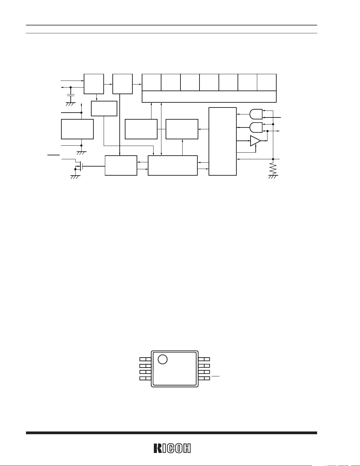
BLOCK DIAGRAM
SEC. MIN. HOUR WEEK DAY
MONTH
YEAR
OSCIN
OSCOUT
VDD
VSS
INTR
OSC DIV
OSC
DETECT
VOLTAGE
REGULATOR
ADDRESS
DECODER
INTERRUPT
CONTROL
SHIFT REGISTER
I/O
CONTROL
ADDRESS
REGISTER
SIO
SCLK
CE
TIME COUNTER
Page 6
RS5C313
3
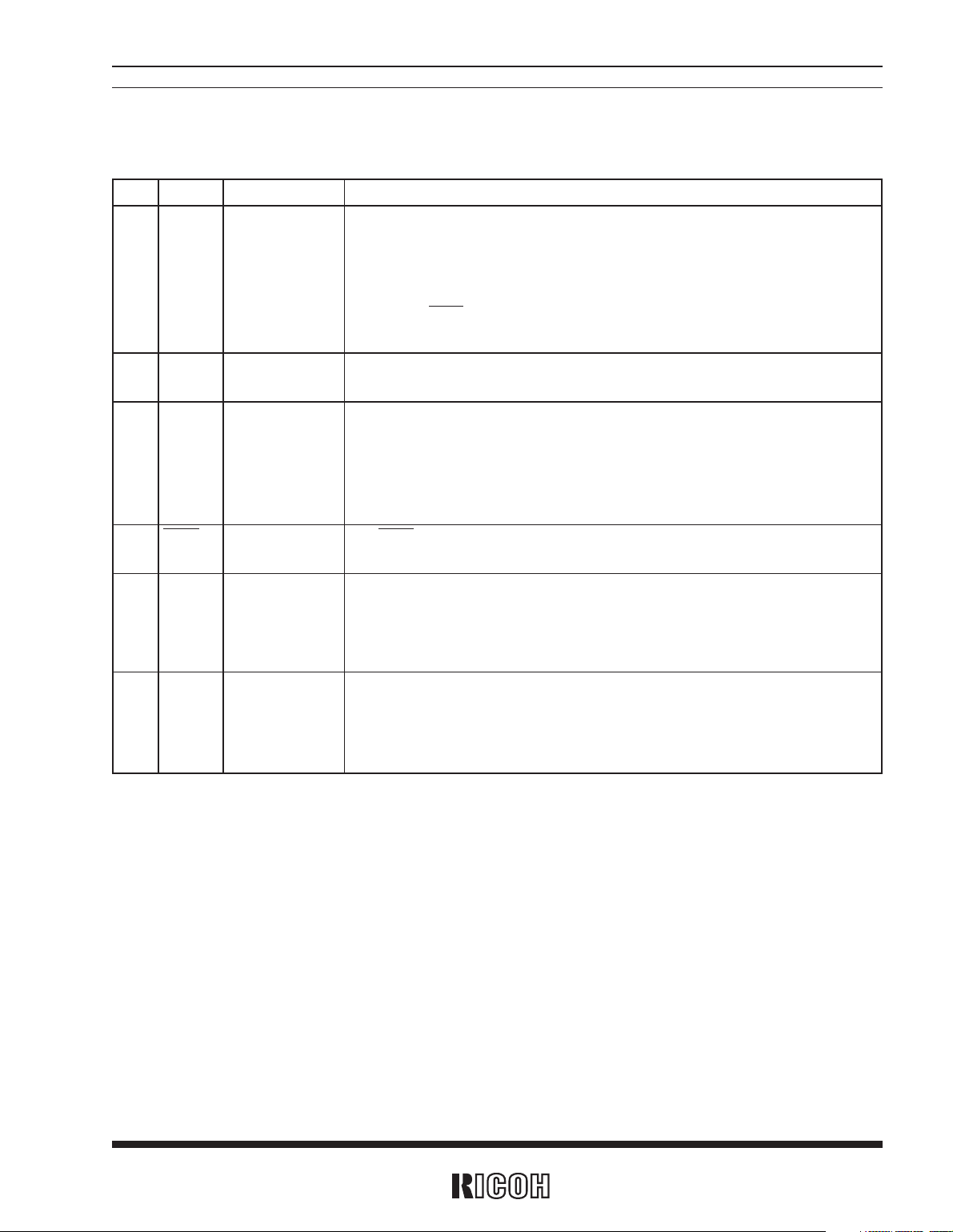
PIN DESCRIPTIONS
Pin No.
Symbol Name Description
1 CE
Chip enable input
The CE pin is used to interface with the CPU and is accessible when held at the high
level. This pin incorporates a pull-down resistor. It should be switched to the low level or opened when not accessed or when powering off the system. Holding the CE
pin at the high level for more than 2.5 seconds forces 1Hz interrupt pulses to be output from the INTR pin for oscillation frequency measurement .
(No pulse is output for less than 1.5 seconds.)
2 SCLK Shift clock input The SCLK pin is used to input shift clock pulses to synchronize data input to, and
output from, the SIO pin.
3 SIO Serial input The SIO pin inputs and outputs written or read data in synchronization with and out-
put shift clock pulses from the SCLK pin. The SIO pin causes high impedance when
the CE pin is held at the low level. After the CE pin is switched to the high level and
the control bits and the address bits are input from the SIO, the SIO pin performs
serial input and output operations
5 INTR Interrupt output The INTR pin outputs cyclic interrupt pulses to the CPU. This pin functions as an
Nch open drain output even when the CE pin is held at the low level.
7 OSCIN
Oscillation circuit
These pins configure an oscillation circuit by connecting a 32.768 kHz crystal
6
OSCOUT
input and output
oscillator between the OSCIN and OSCOUT pins and by connecting a capacitor
between the OSCIN and V
SS pins.
(Any other oscillation circuit components are built into the RS5C313.)
8 V
DD Positive power
supply input The VDD pin is connected to a power supply and the V
SS pin is connected to the
4 V
SS Negative power ground.
supply input
and output
Page 7
RS5C313
4
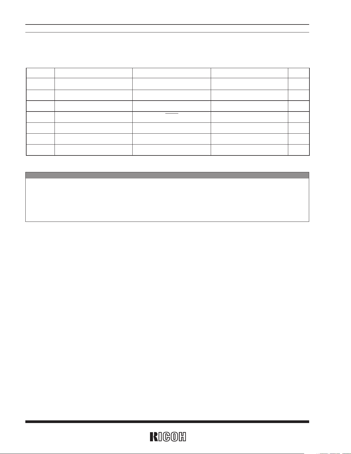
Symbol Item Conditions Ratings Unit
VDD Supply voltage –0.3 to +7.0 V
VI Input voltage –0.3 to +VDD+0.3 V
VO1 Output voltage1 SIO –0.3 to +VDD+0.3 V
VO2 Output voltage2 INTR –0.3 to +12 V
PD Maximum power consumption Topt=25˚C 300 mW
Topt Ambient operating temperature –30 to +80 ˚C
Tstg Storage temperature –40 to +125 ˚C
ABSOLUTE MAXIMUM RATINGS
(VSS=0V)
ABSOLUTE MAXIMUM RATINGS
Absolute Maximum ratings are threshold limit values that must not be exceeded even for an instant under
any conditions. Moreover, such values for any two items must not be reached simultaneously. Operation
above these absolute maximum ratings may cause degradation or permanent damage to the device. These
are stress ratings only and do not necessarily imply functional operation below these limits.
Page 8
RS5C313
5
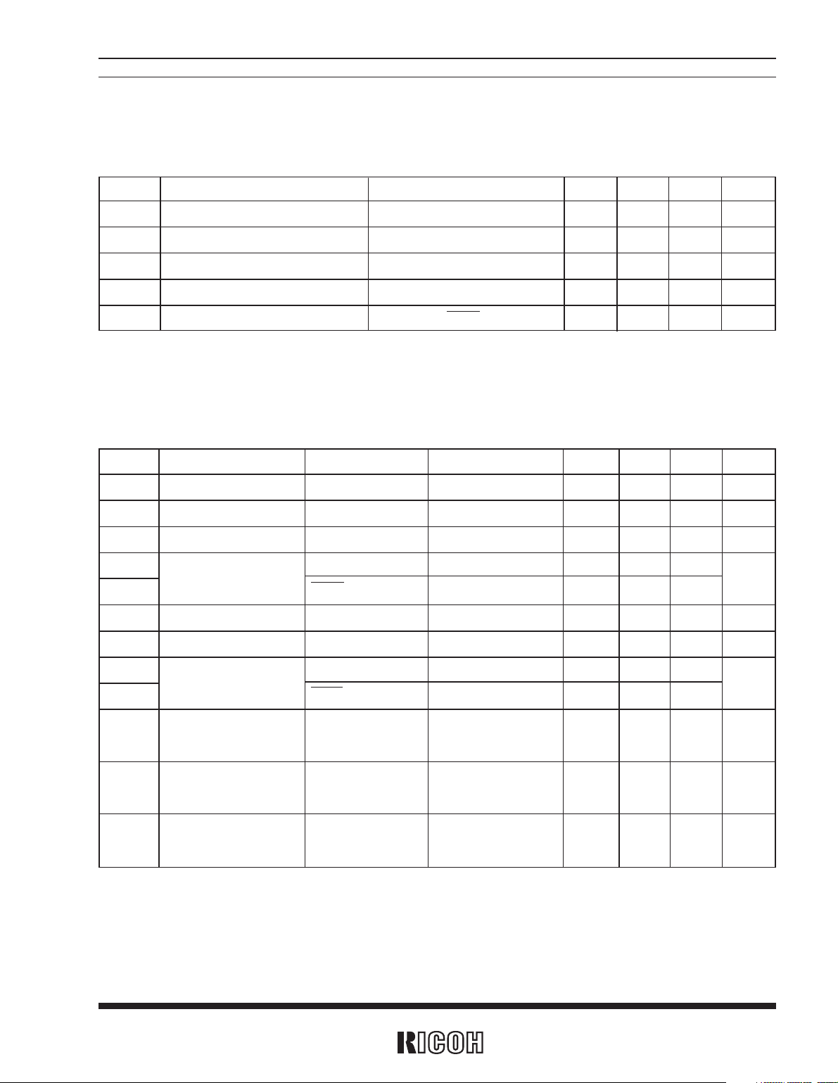
Symbol Item Pin name Conditions MIN. TYP. MAX. Unit
VIH “H” input voltage CE, SCLK, SIO 0.8VDD VDD V
VIL “L” input voltage CE, SCLK, SIO 0 0.2VDD V
IOH “H” output current SIO VOH=VDD–0.5V –1 mA
I
OL1
“L”
output current
SIO V
OL1=0.5V 1
IOL2 INTR VOL2=0.4V 2
RDN Pull-down resistance CE 45 130 450 kΩ
IILK Input leakage current SCLK VI =VDD or VSS –1 1 µA
I
OZ1
Output off-state
SIO V
O=VDD or VSS –2 2
IOZ2
leakage current
INTR V
O=10V –5 5
V
DD=3V
I/O=OPEN
V
DD=5.5V
I/O=OPEN
C
D
Internal oscillator
OSCOUT 10 pF
capacitance
DC CHARACTERISTICS
Unless otherwise specified:VSS=0V, VDD=5V±10%, Topt=–30 to +80˚C, oscillation frequency=32.768kHz (CL=6pF, R1=30kΩ), CG=10pF
IDD1 Power consumption 1 VDD 0.7 1.5 µA
I
DD2 Power consumption 2 VDD 2 µA
mA
µA
Symbol Item Conditions MIN. TYP. MAX. Unit
VDD Operating supply voltage 2.7 5.0 6.0 V
VCLK Time Keeping supply voltage 1.6 6.0 V
fXT Oscillation frequency 32.768 kHz
CG External oscillator capacitance CL value of crystal=6 to 8pF 5 10 24 pF
V
PUP Applied voltage at OFF INTR 10 V
RECOMMENDED OPERATING CONDITIONS
(VSS=0V, Topt=–30 to +80˚C)
Page 9
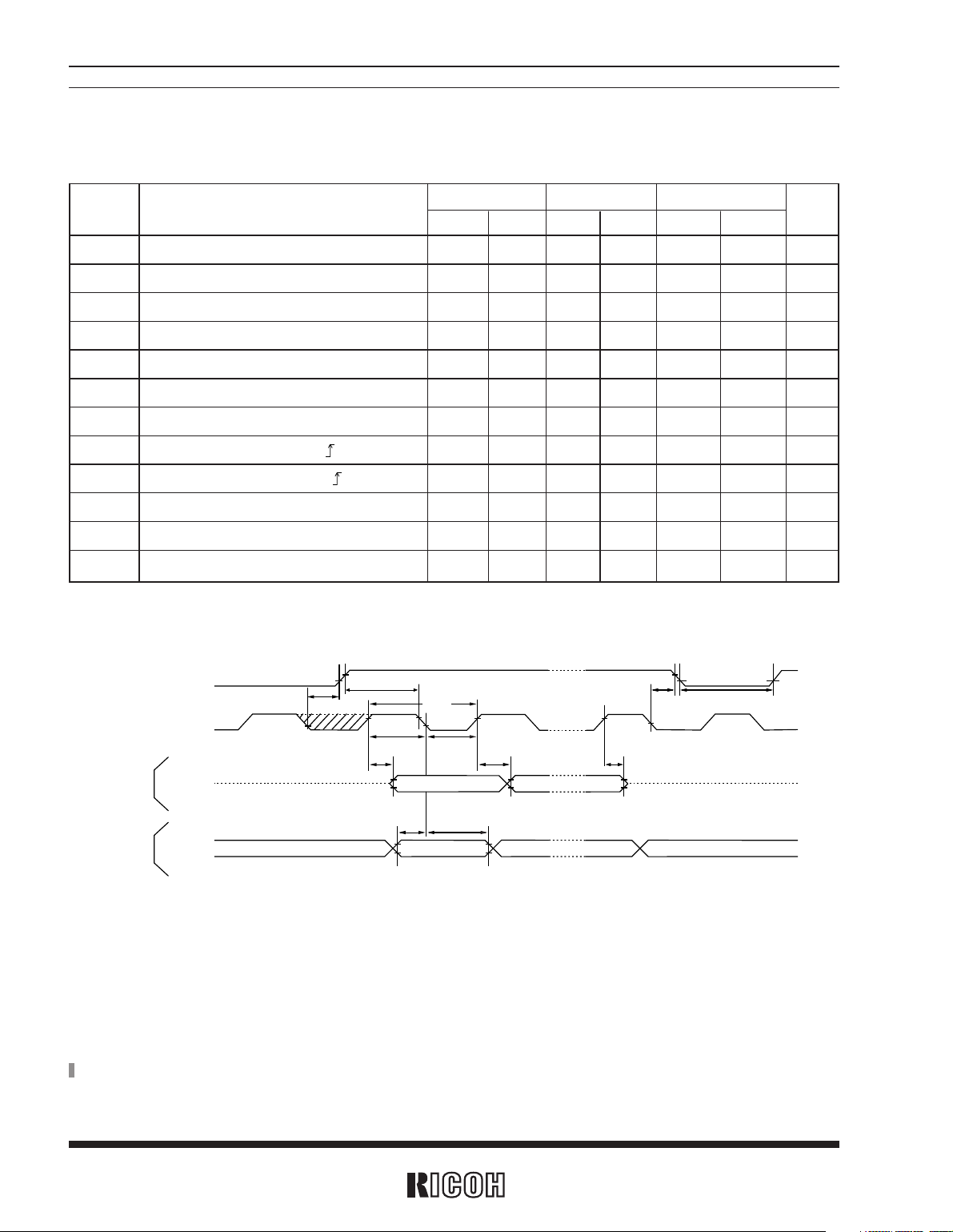
Symbol Item
VDD=5V±10% VDD=3V±10% VDD=5V±20%
Unit
MIN. MAX. MIN. MAX. MIN. MAX.
tCES CE set-up time 175 300 200 ns
tCEH CE hold time 175 300 200 ns
tCR CE recovery time 350 600 400 ns
tSCK SCLK clock cycle 350 600 400 ns
tCKH SCLK “H” clock time 175 300 200 ns
tCKL SCLK “L” clock time 175 300 200 ns
tCKS SCLK clock set-up time 60 100 80 ns
tRE Data output start time (from of SCLK) 120 200 135 ns
tRR Data output delay time (from of SCLK) 120 200 135 ns
tRZ Output floating time 120 200 135 ns
tDS Input data set-up time 50 80 60 ns
tDH Input data hold time 50 50 50 ns
RS5C313
6
AC CHARACTERISTICS
(VSS=0V, Topt=–30 to +80˚C, CL=50pF)
TIMING CHART
Input/output conditions
V
IH = 0.8 × VDD
VIL = 0.2 × VDD
VOH = 0.8 × VDD
VOL = 0.2 × VDD
tSCK
tCES
tCKS
tCEH
tCR
tRE
tRZ
tCKH tCKL
tRR
Read Data
Write Data
t
DS tDH
CE
SCLK
SIORead cycle
Write cycle
SIO
*
) The ability that is fair in “H” or “L” slanted line department
Page 10
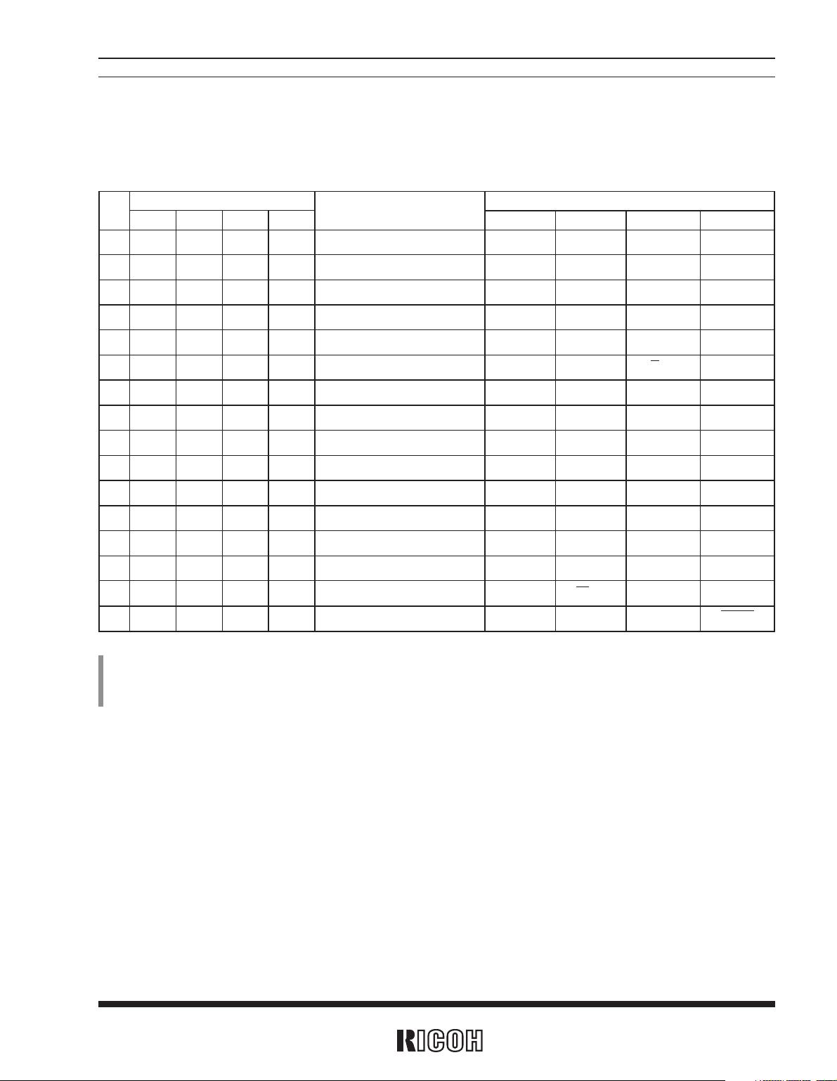
Address
A3
A2 A1 A0
RS5C313
7
0 0 0 0 0 1-second counter S8 S4 S2 S1
1 0 0 0 1 10-second counter S40 S20 S10
2 0 0 1 0 1-minute counter M8 M4 M2 M1
3 0 0 1 1 10-minute counter — M40 M20 M10
4 0 1 0 0 1-hour counter H8 H4 H2 H1
5 0 1 0 1 10-hour counter — —
P/A or H
20 H10
6 0 1 1 0 Day-of-the-week counter — W4 W2 W1
7 0 1 1 1 Interrupt cycle register CT3 CT2 CT1 CT0
8 1 0 0 0 1-day counter D8 D4 D2 D1
9 1 0 0 1 10-day counter — — D20 D10
A 1 0 1 0 1-month counter MO8 MO4 MO2 MO1
B 1 0 1 1 10-month counter — — — MO10
C 1 1 0 0 1-year counter Y8 Y4 Y2 Y1
D 1 1 0 1 10-year counter Y80 Y40 Y20 Y10
E 1 1 1 0 Control register CTFG 12/24
WTEN/XSTP
*3 ADJ/BSY
*
4
F 1 1 1 1 Test register — — — TEST
D3
D2 D1 D0
Data*
1
*
1) All the listed data can be read and written .
*
2) The “—” mark indicates data which can be read only and set to “0” when read .
*
3) The WTEN/XSTP bit of the control register is set to WTEN for write operation and XSTP for read operation.
*
4) The ADJ/BSY bit of the control register is set to ADJ for write operation and BSY for read operation.
Description
1.
Addressing
FUNCTIONAL DESCRIPTIONS
—*
2
Page 11
RS5C313
8
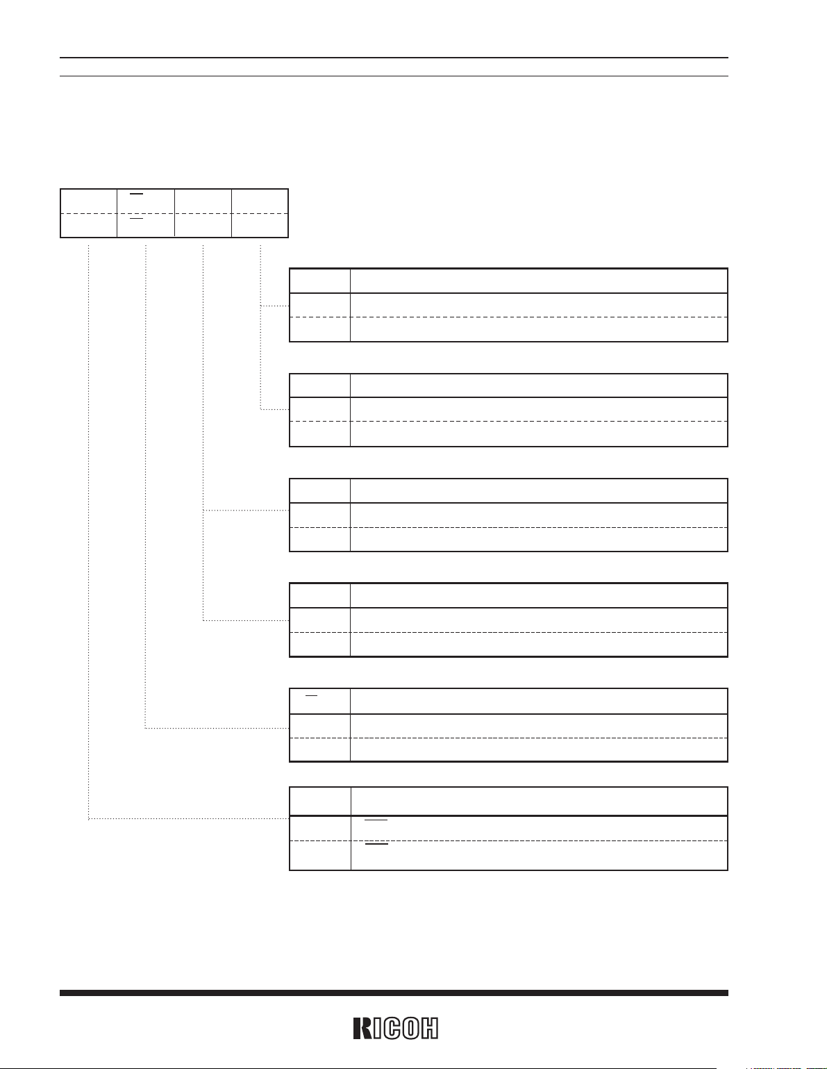
CTFG Description
0
INTR=H(Nch Open Drain). Enabling of write operation when the CT3 bit is set to 1.
1
INTR=L (Nch Open Drain). Enabling of write operation when the CT3 bit is set to 1.
ADJ Description
0 Ordinary operation
1 Second digit adjustment
BSY Description
0 Ordinary operation
1 Second digit carry or adjustment
D3 D2 D1 D0
CTFG 12/24 WTEN ADJ (For write operation)
CTFG 12/24 XSTP BSY (For read operation)
12/24 Description
0 12-hour time display system
(separate for mornings and afternoons)
1 24-hour time display system
2.1-1 (ADJ)
2.1 Control Register (at Eh)
2.
Register
±30-second Adjustment Bit
Clock/Calendar Counter Busy-state Indication Bit
WTEN Description
0 Disabling of 1-second digit carry for clock counter
1 Enabling of 1-second digit carry for clock counter
Clock Counter Enable/Disable Setting Bit
XSTP Description
0 Ordinary oscillation
1 Oscillator halt sensing
Oscillator Halt Sensing Bit
12/24-hour Time Display System Selection Bit
Interrupt Flag Bit
When the ADJ bit is set to 1: (If the WTEN bit is 0, adjustment of second digits is started after the WTEN bit is set to 1.)
1) For second digits ranging from 00 to 29 seconds: Time counts smaller than seconds are reset to set second digits to “00”.
2) For second digits ranging from 30 to 59 seconds: Time counts smaller than seconds are reset to set second digits to “00”
and increment minute digits by 1. After the ADJ bit is set to 1, the BSY
bit is set to 1 for the maximum duration of 122.1µs.
Page 12
Note
RS5C313
9
2.1-2 (BSY)
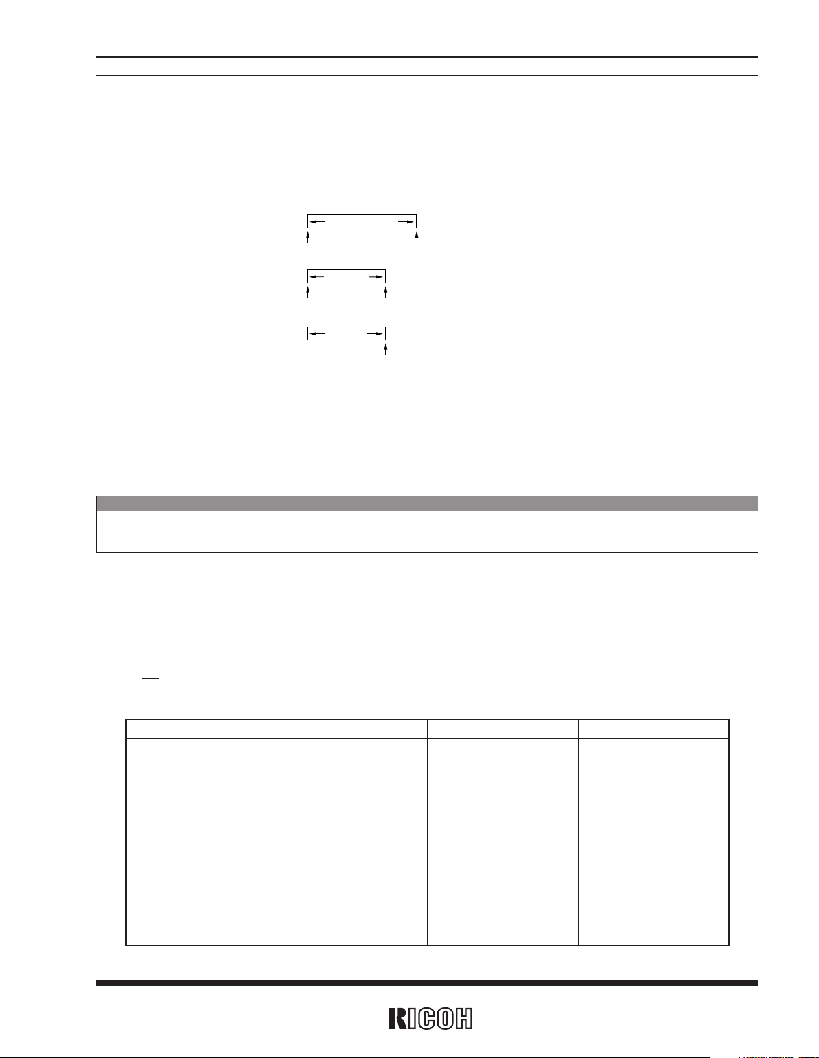
When the BSY bit is 1, the clock and calendar counters are being updated. Consequently, write operation should be performed
for the counters when the BSY bit is 0. Meanwhile, read operation is normally performed for the counters when the BSY bit is 0,
but can be performed without checking the BSY bit as long as appropriate software is provided for preventing read errors(Refer
to the item 11.3 Read Operation from Clock and Calendar Counters). The BSY bit is set to 1 in the following three cases:
MAX. 122.1µs
Setting of the ADJ bit to 1 Completion of second digit adjustment
(1) Adjustment of second digits by
±30 seconds
(2) Second digit increment by 1
(Subject to 1-second digit carry
when the WTEN bit is switched
from 0 to 1)
(3) Ordinary 1-second digit carry
MAX.91.6µs
Setting of the WTEN bit to 1
End of second digit increment by 1
91.6µs
End of second digit carry pulse
2.1-3 (WTEN)
The WTEN bit should be set to 0 to check that the BSY bit is 0 when performing read and write operations for the clock and
calendar counters. For read operation, the WTEN bit may be left as 1 without checking the BSY bit as long as appropriate
measures such as read repetition are provided for preventing read errors(Refer to the item 11.3 Read Operation from Clock
and Calendar Counters). The WTEN bit should be set to 1 after completing read and write operations, or will automatically
be set to 1 by switching the CE pin to the low level. If 1-second digit carry occurs when the WTEN bit is 0, a second digit
increment by 1 occurs when the WTEN bit is set to 1.
2.1-4 (XSTP)
The XSTP bit senses the ocilllator halt. When the CE pin is held at the low level, the XSTP bit is set to 1 once the crystal
oscillator is stopped after initial power-on or supply voltage drop and left to be 1 after it is restarted. When the CE pin is held
at the high level, the XSTP bit is left as it was when the CE pin was held at the low level without checking oscillation stop. As
such, the XSTP bit can be used to validate clock and calendar count data after power-on or supply voltage drop. The XSTP bit
is set to 0 when write operation is performed for the control register (at Eh) (during normal oscillation).
2.1-5 (12/24)
The 12/24 bit specifies time digit display in BCD code.
00 12(AM12) 12 32(PM12)
01 01(AM 1) 13 21(PM 1)
02 02(AM 2) 14 22(PM 2)
03 03(AM 3) 15 23(PM 3)
04 04(AM 4) 16 24(PM 4)
05 05(AM 5) 17 25(PM 5)
06 06(AM 6) 18 26(PM 6)
07 07(AM 7) 19 27(PM 7)
08 08(AM 8) 20 28(PM 8)
09 09(AM 9) 21 29(PM 9)
10 10(AM10) 22 30(PM10)
11 11(AM11) 23 31(PM11)
24-hour time display system 12-hour time display system 24-hour time display system 12-hour time display system
Either the 12-hour or 24-hour time display system should be selected before time setting (e.g. during initialization after power-on).
If the WTEN bit is 0 for 1/1024 second and more, second digit increment by 1 may not occur. (Refer to the item 11.3
Read Operation from Clock and Calendar Counters).
Page 13
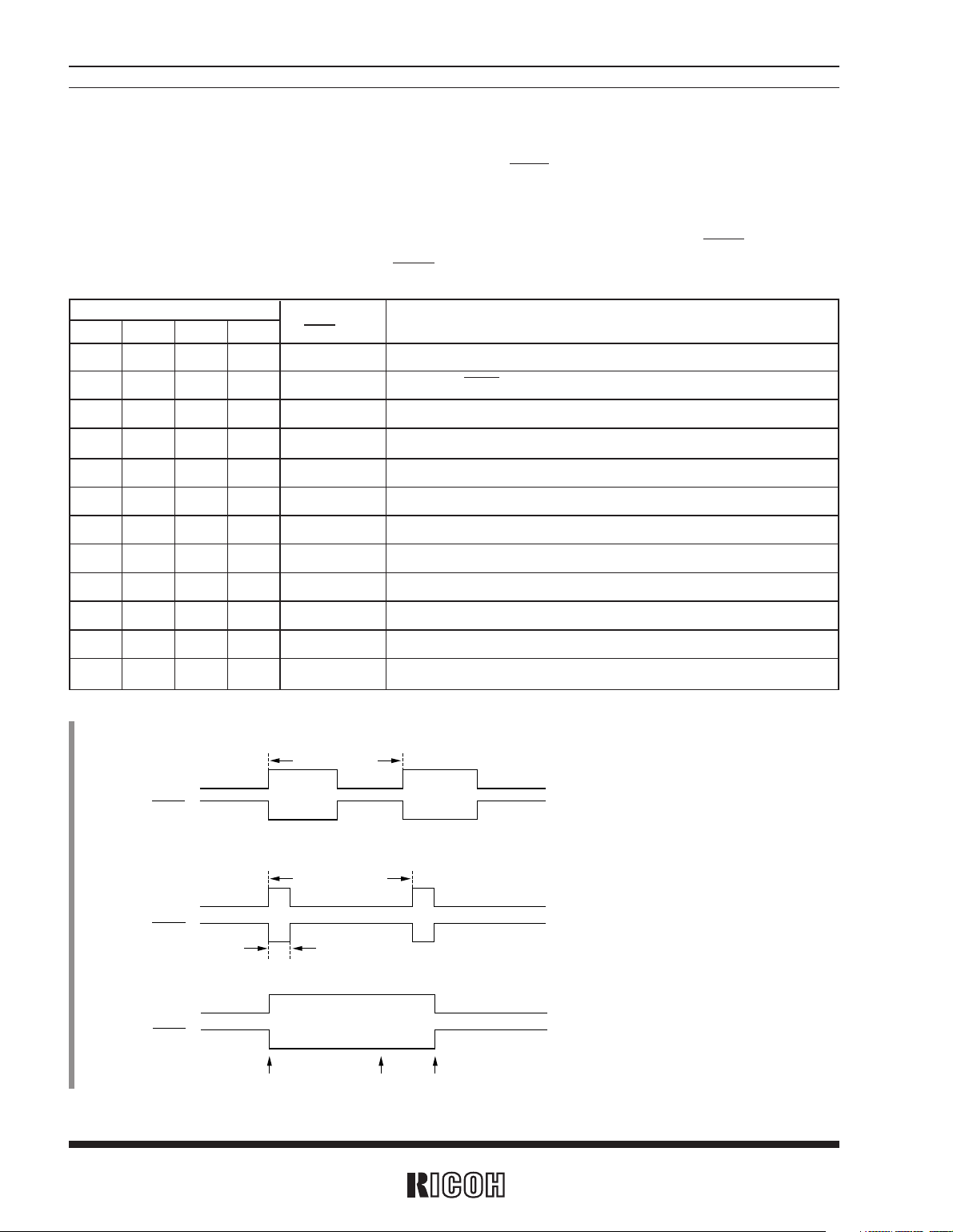
0
*
*
1
0 0 OFF Interrupt disabling
0
*
0 1 ON Fixing INTR pin at low level
0
*
1 0 0.977ms Cycle: 0.977 ms (1/1024 Hz), Duty: 50% *
2
0
*
1 1 0.5s Cycle: 0.5 s (1/2 Hz)*
3
1 0 0 0 1 second Every second*
4
1 0 0 1 10 seconds Every 10 seconds (For display of second digits: 00, 10, 20, 30, 40, and 50)*
4
1 0 1 0 1 minute Every minute (00 second)*
4
1 0 1 1 10 minutes
Every 10 minutes (00 second) (For display of minute digits: 00, 10, 20, 30, 40, and 50)
*
4
1 1 0 0 1 hour Every hour (00 minute and 00 second)*
4
1 1 0 1 1 day Every day (0 hour, 00 minute, and 00 second a.m.)*
4
1 1 1 0 1 week Every week (0 week, 0 hour, 00 minute, and 00 second a.m.)*
4
1 1 1 1 1 month Every month (1st day, 0 hour, 00 minute, and 00 second a.m.)*
4
RS5C313
10
*
1) The symbol “*” in the above table indicates 0 or 1.
Remarks
2.1-6 (CTFG)
The CTFG bit is set to 1 when interrupt pulses are output from the INTR pin held at the low level.
There are two interrupt modes selectable: the pulse mode (when the CT
3 bit is set to 0) and the level mode (when
the CT
3 bit is set to 1).
The CTFG bit can be set only when the CT
3 is set to 1. Setting the CTFG bit to 1 switches the INTR pin to the low
level while setting the CTFG bit to 0 turns off the INTR pin.
0.977ms
CTFG
INTR
Interrupt cycle register
CT
3 CT2 CT1 CT0
Outputs from
INTR pin
0.5s
0.488ms
CTFG
INTR
Interrupt
(Second count-up)
Setting CTFG bit to 0
CTFG
INTR
Interrupt
(Second count-up)
*
2)
*
3)
*
4)
Page 14
RS5C313
11
D3 D2 D1 D0
* * *
TEST (For write operation)
0 0 0 0 (For read operation)
*
1
TEST Description
0 Testing mode
1 Ordinary operating mode
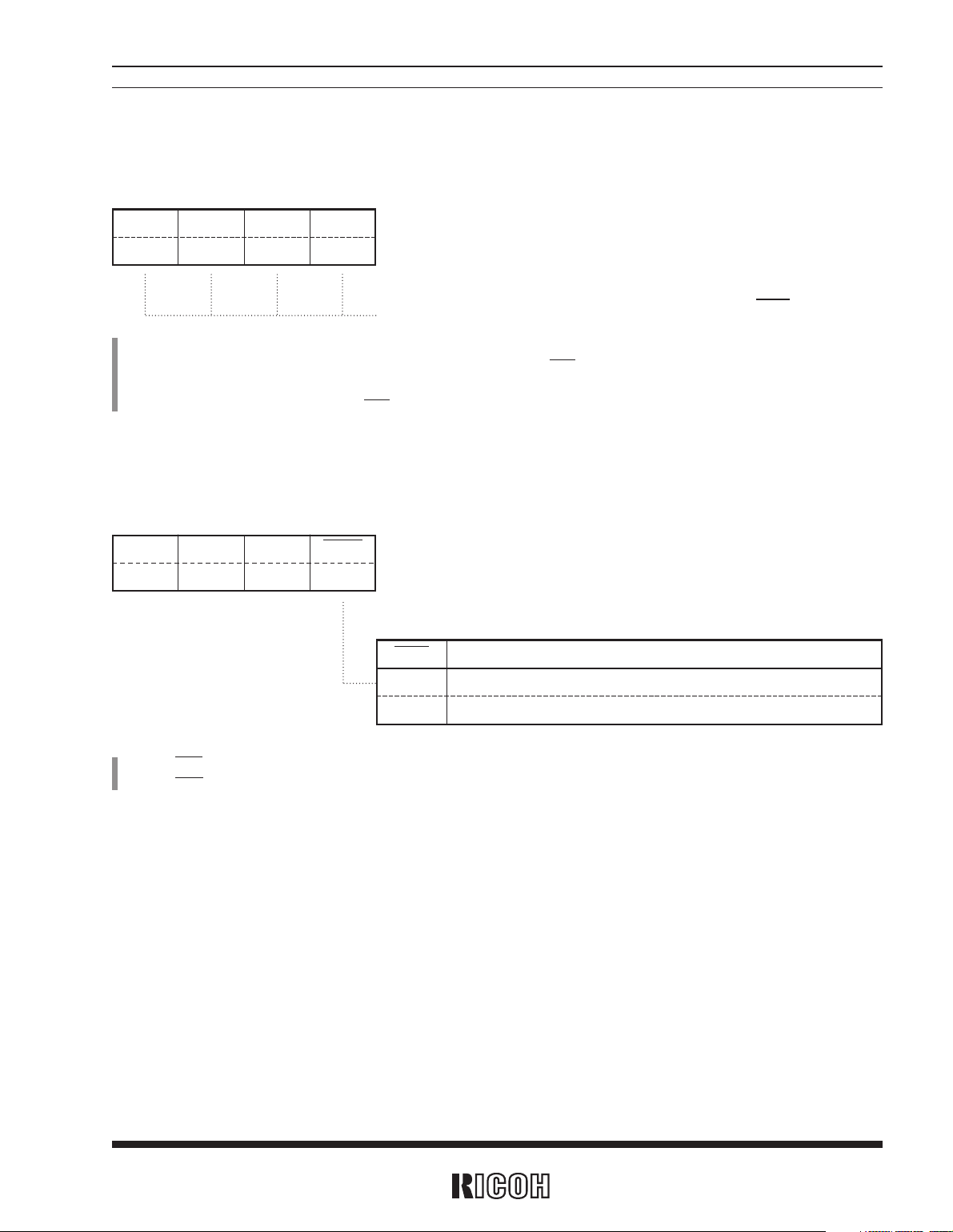
2.2 Interrupt Cycle Register (at 7h)
D3 D2 D1 D0
CT3 CT2 CT1 CT0 (For write operation)
CT3 CT2 CT1 CT0 (For read operation)
Bits for selecting the interrupt cycle and output mode at the INTR pin
*
1
Bit For Testing*
2
*
1) (CT3 to CT0)
The CT
3 to CT0 bits are used to select the interrupt cycle and output mode at the INTR pin. There are two interrupt modes selectable: the pulse mode
(when the CT
3 bit is set to 0) and the level mode (when the CT3 bit is set to 1).
The interrupt cycle and output mode at the INTR pin are shown in detail in the section on the CTFG bit in “2.1 Control Register (at Eh)”.
2.3 Test Register (at Fh)
*
1) The TEST bit is write-only and set to 0 when read.
*
2) The TEST bit should be fixed at 1 for ordinary operation and will automatically be set to 1 when the CE pin is at the low level.
Page 15
RS5C313
12
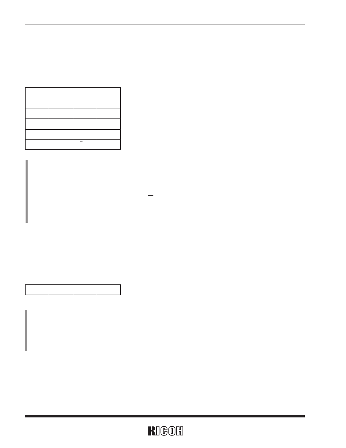
D3 D2 D1 D0
*
W4 W2 W1 ( read and write cycle) Day-of-the-week counter
1) The “*” mark in the above table indicates data which are set to 0 for read cycle and not set for write cycle.
2) Any carry to 1-second digits from the second counter is disabled when the WTEN bit (of the control register) is set to 0.
3) Time digit display ( BCD code):
Second digits: Range from 00 to 59 and carried to minute digits when incremented from 59 to 00.
Minute digits: Range from 00 to 59 and carried to hour digits when incremented from 59 to 00.
Hour digits: Range as shown in the section on the 12/24 bit and carried to day and day-of-the-week.
digits when incremented from 11 p.m. to 12 a.m. or 23 to 00.
4) Any registered imaginary time should be replaced with actual time as carrying to such registered imaginary time digits from
lower-order ones cause the clock counter to malfunction.
D3 D2 D1 D0
S8 S4 S2 S1 ( read and write cycle) 1-second time digit (at 0h)
*
S40 S20 S10 (read and write cycle) 10-second time digit (at 1h)
M8 M4 M2 M1 (read and write cycle) 1-minute time digit (at 2h)
*
M40 M20 M10 (read and write cycle) 10-minute time digit (at 3h)
H8 H4 H2 H1 (read and write cycle) 1-hour time digit (at 4h)
* *
P/A or H
20
H10 (read and write cycle) 10-hour time digit (at 5h)
3.1 Clock Counter (at 0h to 5h)
3. Counters
1) The “*” mark in the above table indicates data which are set to 0 for read cycle and not set for write cycle.
2) Day-of-the-week digits are incremented by 1 when carried to 1-day digits.
3) Day-of-the-week digit display (incremented in septimal notation):
(W4W2W1)=(000)→ (001)→ - - - - - - → (110) → (000)
The relation between days of the week and day-of-the-week digits is user changeable (e.g. Sunday=000).
4) The (W4W2W1) should not be set to (111).
3.2 Day-of-the-week Counter (at 6h)
Page 16
RS5C313
13
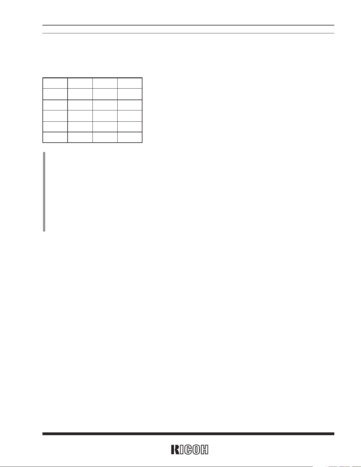
1) The “*” mark in the above table indicates data which are set to 0 for read cycle and not set for write cycle.
2) The automatic calendar function provides the following calendar digit displays in BCD code:
Day digits: Range from 1 to 31 (for January, March, May, July, August, October, and December).
Range from 1 to 30 (for April, June, September, and November).
Range from 1 to 29 (for February in leap years).
Range from 1 to 28 (for February in ordinary years).
Carried to month digits when cycled to 1.
Month digits: Range from 1 to 12 and carried to year digits when cycled to 1.
Year digits: Range from 00 to 99 and counted as 00, 04, 08, - - - -- -, 92, and 96 in leap years.
3) Any registered imaginary time should be replaced with actual time as carrying to such registered imaginary time digits from
lower-order ones cause the clock counter to malfunction.
D3 D2 D1 D0
D8 D4 D2 D1 (read and write cycle) 1-day calendar digit (at 8h)
* *
D20 D10 (read and write cycle) 10-day calendar digit (at 9h)
MO8 MO4 MO2 MO1 (read and write cycle) 1-month calendar digit (at Ah)
* * *
MO10 (read and write cycle) 10-month calendar digit(at Bh)
Y8 Y4 Y2 Y1 (read and write cycle) 1-year calendar digit (at Ch)
Y80 Y40 Y20 Y10 (read and write cycle) 10-year calendar digit (at Dh)
3.3 Calendar Counter (at 8h to Dh)
Page 17
RS5C313
14
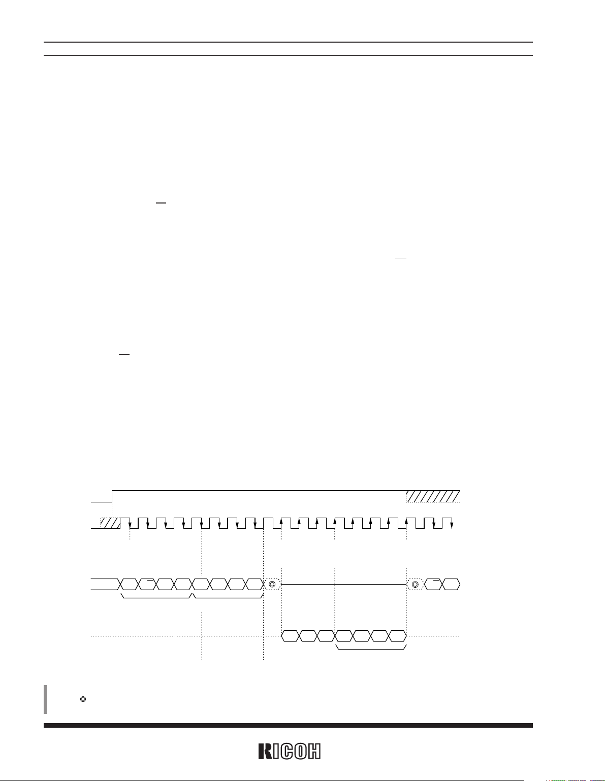
The real-time clock becomes accessible by switching the CE pin from the low level to high level to enable interfacing with the CPU and then inputting setting data (control bits and address bits) to the SIO pin in synchronization
with shift clock pulses from the SCLK pin.
The input data are registered in synchronization with the falling edge of the SCLK. When the data is read, the read
cycle shall be set by control bits.
1.1 Read Cycle Flow
1. The CE pin is switched from the low level to the high level.
2. Four control bits (with the first bit ignored) and four read address bits are input from the SIO pin. At this time,
control bits R/W and AD are set equally to 1 while a control bit DT is set to 0.
3. The SIO pin enters the output mode at the rising edge of the shift clock pulse 2B from the SCLK pin while the
four read bits (MSB→LSB) at designated addresses are output at the rising edge of the shift clock pulse 5B (see
the figure below).
4. Then, the SIO pin returns to the input mode at the rising edge of the shift clock pulse 1C. Afterwards control bits and
address bits are input at the shift clock pulses 1C in the same manner as at the shift clock pulse 1A.
5. At the end of read cycle, the CE pin is switched from the high level to the low level (after
tCEH from the falling edge of
the eighth shift clock pulse from the SCLK pin). (Following on read cycle, write operation can be performed by setting
control bits in the write mode at the shift clock pulse 1C and later with the CE pin held at the high level.)
R/W: Establishes the read mode when set to 1, and the write mode when set to 0.
AD: Writes succeeding address bits (A3 to A0) to the address register when set to 1 with the
DT bit set to 0 and performs no such write operation in any other case.
DT: Writes data bits (D3 to D0) to the counter or register specified by the address register
which has written just before when set to 1 with the R/W and AD bits set equally to 0 and
performs no such write operation in any other case.
A3 to A0: Inputs the bits MSB to LSB in the address table describing the functions.
• Control bits
• Address bits
USAGES
1. Read Data
1A 2A 3A 4A 5A 6A 7A 8A 1B 2B 3B 4B 5B 6B 7B 8B 1C 2C 3C
R/W
AD DT A3 A2 A1 A0
— — — D3 D2 D1 D0
R/W
AD
*
CE
SCLK
Input to
SIO pin
Output from
SIO pin
(Internal processing)
Reading to shift register
Writing to
address register
Setting of
control bits
Control bits Address bits
(Hi-z) (Hi-z)
(Hi-z)
Read data
Setting of
SIO pin in
output mode
Shifting data
Setting of SIO pin in
input mode
*
*
) In the above figure, the “*”mark indicates arbitrary data; the “—” mark indicates unknown data;
the mark indicates data which are available when the SIO pin is held at the high, low, or Hiz level ;
and the diagonaliy shaded area indicates high or low.
“ ”
Page 18
RS5C313
15
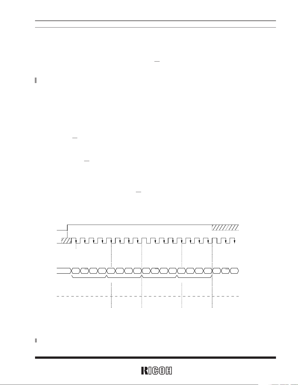
Writing data to the real-time clock requires inputting setting data (control bits and address bits) to the SIO pin and
then establishing the write mode by using a control bit R/W in the same manner as in read operation.
*
) Control bits and address bits are described in the previous section on read cycle.
• Data bits D3 to D0 : inputs writing data to the counter or the register describing the functions in order of MSB
to LSB.
2.1 Write Cycle Flow
1. The CE pin is switched from the low level to the high level.
2. Four control bits (with the first bit ignored) and four write address bits are input from the SIO pin. At this time,
control bits R/W and DT are set equally to 0 while a control bit AD is set to 1 (at the shift clock pulses 1A to 8A
from the SCLK pin).
3. Four control bits and four bits of data to be written are input in the descending order of their significance. At this
time, control bits R/W and AD are set equally to 0 while a control bit DT is set to 1 (at the shift clock pulses 1B
to 8B from the SCLK pin).
4. When write cycle is continued, control bits and address bits are input at the shift clock pulse 1C and later in the
same manner as at the shift clock pulse 1A.
5. At the end of write operation, control bits R/W, AD, and DT are set equally to 0 (at the falling edge of the fifth
shift clock pulse and later from the SCLK pin) or the CE pin is switched from the high level to the low level (after
tCEH from the falling edge of the eighth shift clock pulse from the SCLK pin).
2.
Write Data
1A 2A 3A 4A 5A 6A 7A 8A 1B 2B 3B 4B 5B 6B 7B 8B 1C 2C 3C
R/W
AD DT A3 A2 A1 A0
R/W AD DT D3 D2 D1 D0
R/W
AD
*
CE
SCLK
Input to
SIO pin
Output from
SIO pin
(Internal processing)
Reading from shift register
Writing to
address register
Setting of
control bits
End of write operationSetting of
control bits
Control bits Address bits
Control bits Data bits
(Hi-z) (Hi-z)
*
*
*
*
) In the above figure, the “*” mark indicates arbitrary data; and the diagonally shaded area indicates the high or low level.
Page 19
Considerations
When the power turns on from 0V, the CE pin should be set low or open once.
RS5C313
16
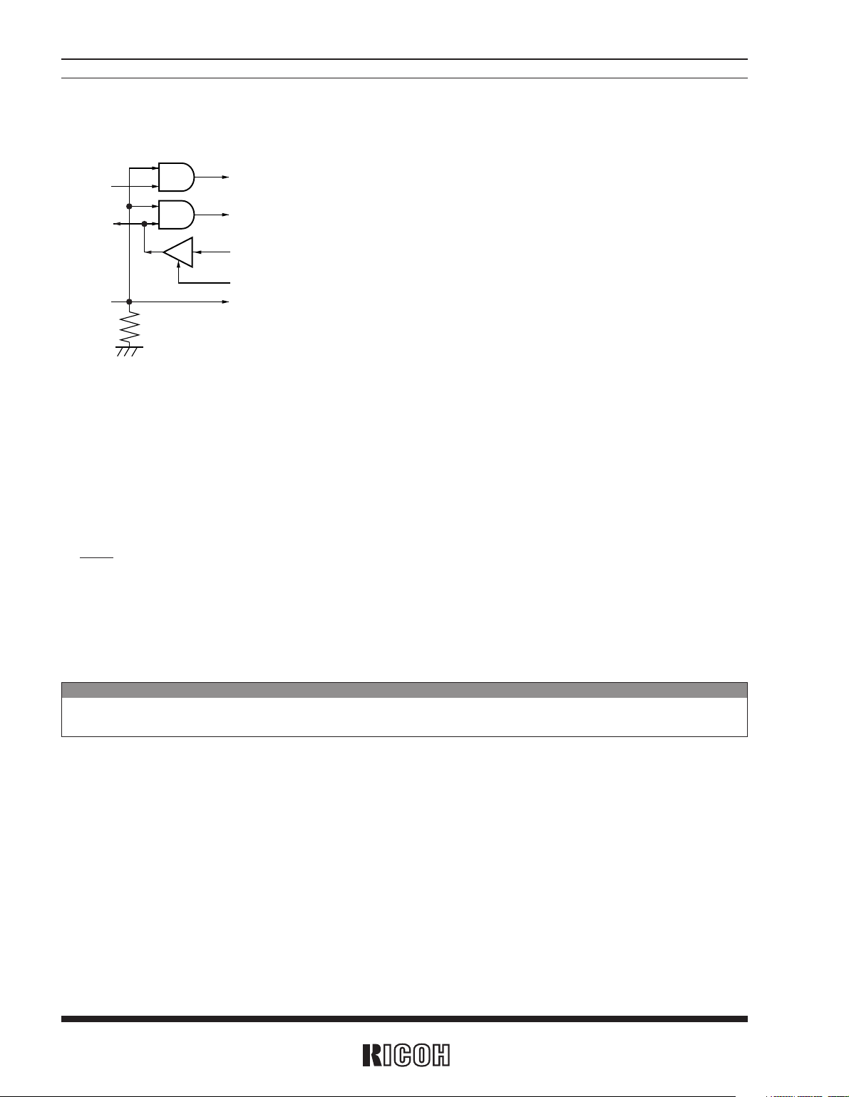
1) Switching the CE pin to the high level enables both the SCLK and SIO pins, allowing data to be serially read from and
written to the SIO pin in synchronization with shift clock pulses input from the SCLK pin.
2) Switching the CE pin to the low level or opening it disables both the SCLK and SIO pins, causing high impedance and
resetting the internal interfacing circuits such as the shift register.
3) The CE pin should be held at the low level or open state when no access is made to the RS5C313. The CE pin incorporates a pull-down resistor.
4) During system power-down (being back-up battery powered), the low-level input of the CE pin should be brought as close
as possible to the VSS level to minimize the loss of charge in the battery.
5) Holding the CE pin at the high level for more than 2.5 seconds mainly forces 1Hz interrupt pulses to be output from the
INTR pin for oscillation frequency measurement. When the CE pin is held at the high level for less than 1.5 seconds, no
pulse is output.
6) The CE pin should be held at the low level in order to enable oscillator halt sensing. Holding the CE pin at the high level,
therefore, disables oscillator halt sensing, retaining the value of the XSTP (oscillator halt sensing) bit which exists immediately before the CE pin is switched to the high level.
3. CE Pin
SCLK
SIO
CE
Shift clock pulses
Address & Write data
Read data
Reading control bits
Control bits
Page 20
Other Relevant Considerations
1) When applying an external input of clock pulses (32.768 kHz) to the OSCIN pin:
DC coupling - - - - - Prohibited due to mismatching input levels.
AC coupling - - - - - Permissible except that unpredictable results may occur in oscillator halt sensing due to
possible sensing errors caused by noises, etc.
2) Avoid using the oscillator output of the RS5C313 (from the OSCOUT pin) to drive any other IC for the purpose of
ensuring stable oscillation.
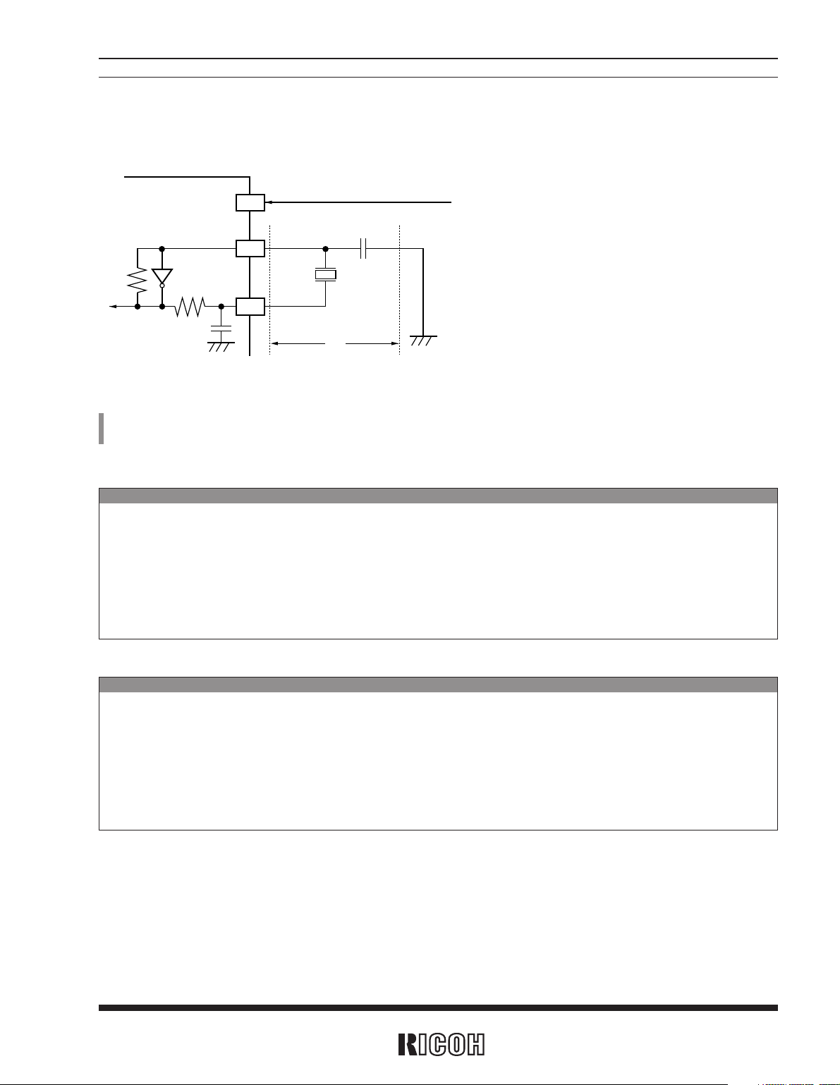
Considerations in Mounting Components Surrounding Oscillating Circuit
1) Mount the crystal oscillators and C
G in the closest possible position to the IC.
2) Avoid laying any signal or power line close to the oscillation circuit (particularly in the area marked with “←A →”
in the above figure).
3) Apply the highest possible insulation resistance between the OSCIN or OSCOUT pin and the PCB.
4) Avoid using any long parallel line to wire the OSCIN or OSCOUT pin.
5) Take extreme care not to cause condensation, which leads to various problems such as oscillation halt.
RS5C313
17
4.
Configuration of Oscillating Circuit
RF
RD
CD
OSCIN
OSCOUT
32kHz
VDD
VDD
C
G
VSS
A
8
7
6
Typical external device:
X'tal : 32.768kHz
(R
1=30kΩ)
(C
L=6pF to 8pF)
C
G=8pF to 20pF
Standard values of internal devices:
R
F=15MΩ
(
TYP.
)
R
D=60kΩ (TYP.
)
C
D=10pF (TYP.)
The oscillation circuit is driven at a constant voltage of about 1.5 V relative to the V
SS level. Consequently, it generates a wave-
form having a peak-to-peak amplitude of about 1.5 V on the positive side of the V
SS level.
Page 21
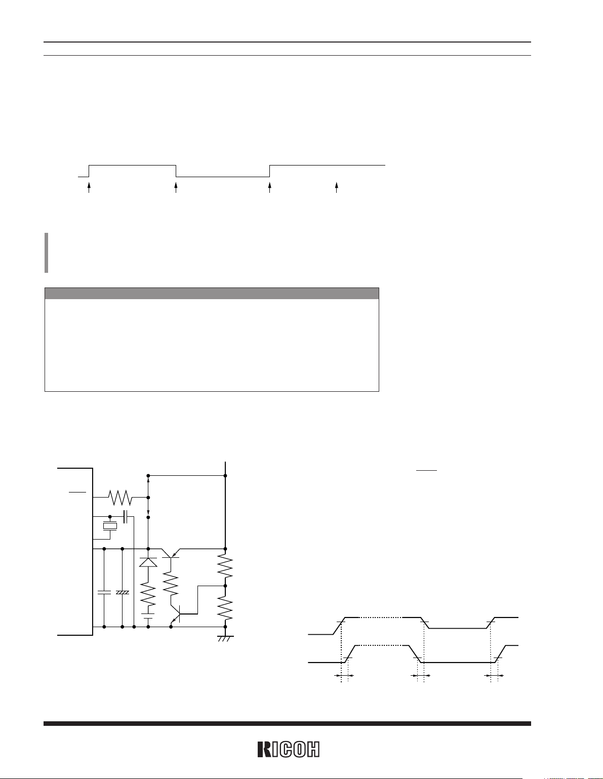
Considerations in Use of XSTP Bit
Ensure error-free oscillation halt sensing by preventing the following:
1) Instantaneous disconnection of V
DD
2) Condensation on the crystal oscillator
3) Generation of noise on the PCB in the crystal oscillator
4) Application of voltage exceeding prescribed maximum ratings to the individual pins of the IC
RS5C313
18
Oscillation Halt can be sensed by setting the XSTP (oscillator halt sensing) bit to 0 (after writing data to the control
register) and then monitoring the XSTP bit. Upon oscillator halt sensing, the XSTP bit is switched from 0 to 1. This
function can be applied to judge clock data validity.
5. Oscillator Halt Sensing
Writing of data to
control register
(in the presence of oscillation)
Power-on
from 0V
*
1
Oscillation restart
*
2
Oscillation halt
XSTP
*
1) While the CE pin is held at the low level the XSTP bit is set to 1 upon power-on from 0 V. Note that any instantaneous power disconnection may
cause operational failure. When the CE pin is held at the high level oscillation halt is not sensed and the value of the XSTP bit when the CE pin is
held at the low level is retained.
*
2) Once oscillation halt has been sensed, the XSTP bit is held at 1 even if oscillation is restarted.
6.
Typical Power Supply Circuit
OSCIN
OSCOUT
VDD
VSS
RS5C313
B
A
System supply voltage
INTR
1) Connect the capacitance of the oscillation circuit to the VSS pin.
2) Mount the high- and low-frequency by-pass capacitors in parallel
and very close to the RS5C313.
3) Connect the pull-up resistor of the INTR pin to two different positions depending on whether the resistor is in use during battery
back-up.
• When not in use during battery back-up
- - - - - Position A in the left figure
• When in use during battery back-up
- - - - - Position B in the left figure
4) Timing of power supply on / off and CE terminal refer to lower part
plan.
C
0V
V
DD
CE
D
0.2V
DD
MIN. 0µs MIN. 0µs MIN. 0µs
C,D,E : The lower limit voltage for CPU operation
0.2V
DD 0.2VDD
Battery voltage
System supply
voltage
E
Page 22
RS5C313
19
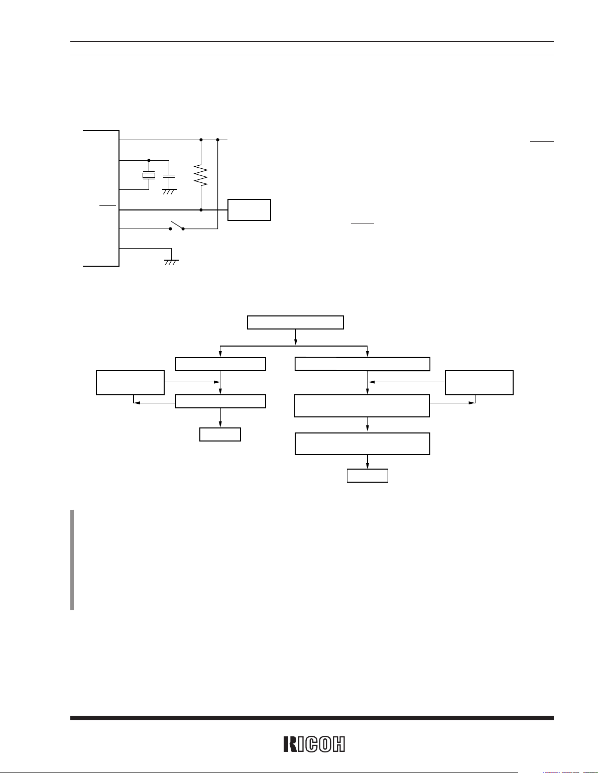
7.1 Oscillation Frequency Measurement
7.
Oscillation Frequency Adjustment
INTR
OSCOUT
OSCIN
VDD
CE
VSS
32kHz
+5V or +3V
Frequency
counter
C
G
1) When switch the CE pin to the high level after low level or
open state, a 1-Hz interrupt pulse is output from the INTR
pin about 2.5 seconds later. Measure this interrupt pulse by
using a frequency counter
2) Ensure that the frequency counter has more than six digits
(on the order of 1 ppm).
3) Place the C
G between the OSCIN pin and the VSS level and
pull up the INTR pin output to the V
DD .
*
1) To ensure that the crystal is matched to the IC, inquire its crystal supplier about its CL (load capacitance) and R1 (equivalent series resistance) values. It is recommended that the crystal should have the C
L value range of 6 to 8pF and the typical R1 value of 30k ohms.
*
2) To allow for the possible effects of floating capacitance, select the optimum capacitance of the CG on the mounted PCB. The standard and recommendable capacitance values of the C
G range from 5 to 24pF and 8 to 20pF, respectively. When you need to change the frequency to get higher
accuracy, change the C
L value of the crystal.
*
3) Collate the central variable capacitance value of the CG with its oscillation frequency by adjusting the angle of rotation of the variable capacitance of
the C
G in such a manner that the actual variable capacitance value is slightly smaller than the central variable capacitance value. (It is recommended
that the central variable capacitance value should be slightly less than one half of the actual variable capacitance value because the smaller is variable capacitance, the greater are fluctuations in oscillation frequency.) In the case of an excessive deviation of the oscillation frequency from its
required value, change the C
L value of the crystal.
7.2 Oscillation Frequency Adjustment
Select crystal oscillator
NG
OK
OK
NG
Fix CG.
(For fixed capacitance)
(For variable capacitance)
Change C
L
value of crystal.
Optimize CG.
End
End
Fix the capacitance of CG.
Optimize central variable
capacitance value
Make fine frequency adjustment
with variable capacitance.
Change the CL
value of crystal.
*
1
*
3
*
3
*
2
Page 23
Note
Any rise or fall in ambient temperature from its reference value ranging from
20 to 25 degrees Celsius causes a time delay for a 32kHz crystal oscillator. It is
recommendable, therefore, to set slightly high oscillation frequency at room
temperature.
0
*
*
1
0 0 OFF Interrupt halt
0
*
0 1 ON Fixing the INTR pin at the low level
0
*
1 0 0.977ms Cycle: 0.977ms (1/1024Hz) Duty: 50%
0
*
1 1 0.5s Cycle: 0.5s (1/2Hz)
1 0 0 0 1 second Every second
1 0 0 1 10 seconds Every 10 seconds (For display of second digits: 00, 10, 20, 30, 40, and 50)
1 0 1 0 1 minute Every minute (00 second)
1 0 1 1 10 minutes
Every 10 minutes (00 second) (For display of minute digits: 00, 10, 20, 30, 40, and 50)
1 1 0 0 1 hour Every hour (00 minute and 00 second)
1 1 0 1 1 day Every day (0 hour, 00 minute, and 00 second a.m.)
1 1 1 0 1 week Every week (0 week, 0 hour, 00 minute, and 00 second a.m.)
1 1 1 1 1 month Every month (1st day, 0 hour, 00 minute, and 00 second a.m.)
RS5C313
20
After adjustment, oscillation frequency is subject to fluctuations of an ambient temperature and supply voltage.
See “10. Typical Characteristic Measurements”.
Remarks
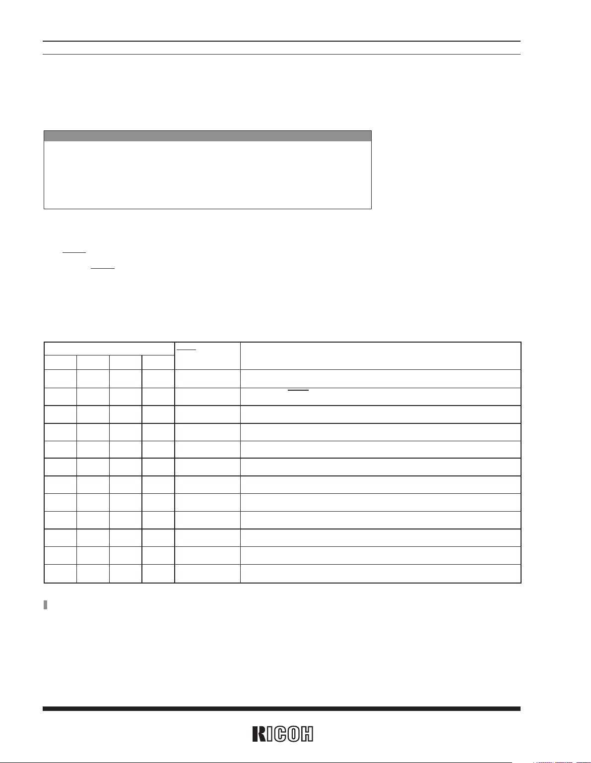
8.1 Selection of Interrupt Cycle
The interrupt cycle register can be used to select either one of two interrupt output modes: the pulse mode (when
the CT
3 bit is set to 0) and the level mode (when the CT3 bit is set to 1).
Interrupt cycle register
CT3 CT2 CT1 CT0
INTR pin output
The INTR pin output, the interrupt cycle register, and the CTFG bit can be used to interrupt the CPU in a certain
cycle. (The INTR pin functions as an Nch open drain output.)
8. Interrupt Operation
*
1) The symbol “*” in the above table indicates 0 or 1.
Page 24
RS5C313
21
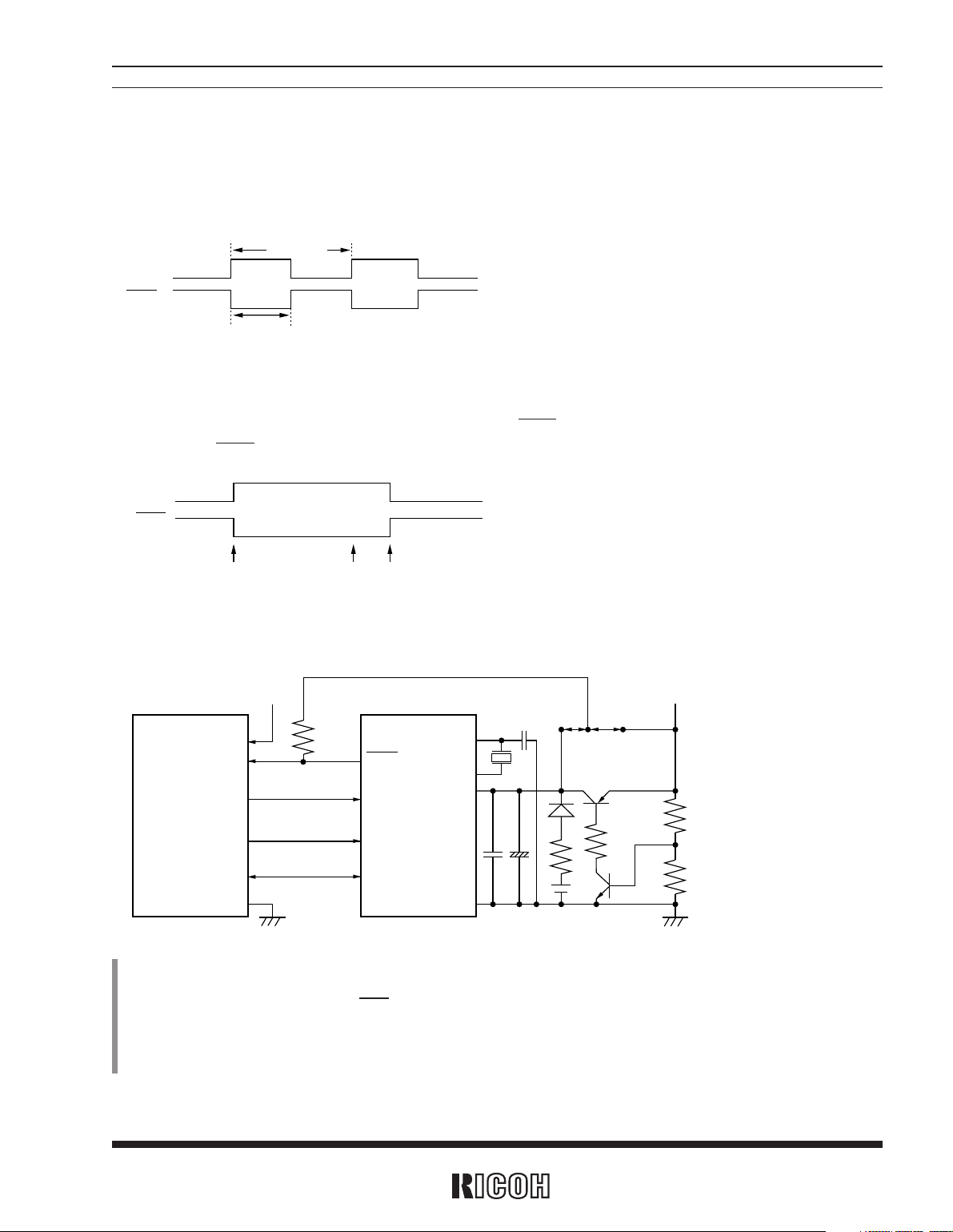
9.
Typical Application
VCC
VSS
OSCIN
OSCOUT
VDD
VSS
INTR
CE
SCLK
SIO
CPU RS5C313
System supply
voltage
B A
System supply
voltage
1) Connect the capacitance of the oscillation circuit to the VSS pin.
2) Mount the high- and low-frequency by-pass capacitors in parallel and very close to the RS5C313.
3) Connect the pull-up resistor of the INTR pin to two different positions depending on whether the resistor is in use during battery back-up.
When not in use during battery back-up - - - - - Position A in the above figure
When in use during battery back-up - - - - - - -- Position B in the above figure
8.2 Pulse Mode Interrupt
When the CT3 bit is set to 0 and provides four interrupt cycles, off, on, 1024 Hz, and 2 Hz can be selected. The
CTFG bit cannot be set because it is used for output monitoring.
T1
0.488ms
CTFG
INTR
8.3 Level Mode Interrupt
When the CT3 bit is set to 1, clock-interlocked cycles in increments of 1 second to 1 month can be selected. The
CTFG bit can be written; writing the CTFG bit switches the INTR pin to the low level while writing 0 to the CTFG
bit turns off the INTR pin.
Interrupt
(Second count-up)
Writing 0 to CTFG bit
CTFG
INTR
Interrupt
(Second count-up)
1024Hz : T1=0.977ms
2Hz : T1=500ms
Page 25
RS5C313
22
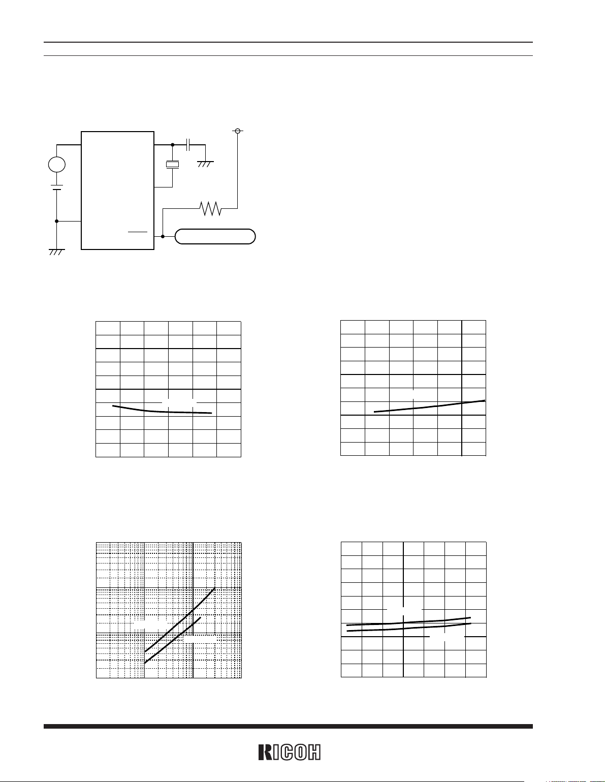
10.
Typical Characteristic Measurements
OSCIN
OSCOUT
INTR
VSS
VDD
A
CG
X'tal
VDD
Frequency counter
10.1 Standby Current vs. CG (VDD=3V) 10.2 Standby Current vs. VDD(CG=10pF)
VDD=3V
Standby Current IDD (µA)
CG (pF)
0
2.0
1.0
0.0
Topt=25˚C
30
20
10
CG=10pF
VDD (V)
Standby Current IDD (µA)
Topt=25˚C
2.0
1.0
0.0
0 2 4
6
CG=10pF
X'tal : R
1=30kΩ, CL=6pF
T
opt=25˚C
Input pin : V
DD or VSS
Output pin : Open
10.3 Operational Current vs. SCLK Frequency 10.4 Standby Current vs. Temperature (VDD=3V, 5V)
VDD=3V
VDD=5V
SCLK Frequency (MHz)
Operational Current IOPR (mA)
Topt=25˚C
1
0.1
0.01
0.001
0.01
0.1
1 10
VDD=3V
VDD=5V
Temperature Topt (˚C)
Standby Current IDD (µA)
CG=10pF
2
1
0
–40 –20 0
20
40 60 80
100
Page 26
RS5C313
23
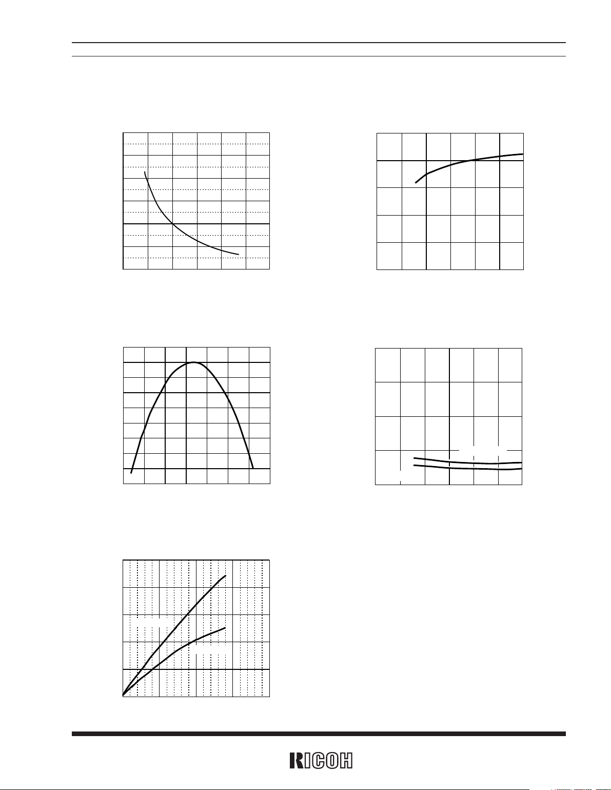
10.5 Oscillation Frequency Deviation vs. CG
(f0: CG=10pF reference)
10.6 Oscillation Frequency Deviation vs. V
DD
(f0: VDD=4V reference)
10.7
Oscillation Frequency Deviation vs. T emperature
(f0: Topt=25˚C reference)
10.8 Oscillation Start Time vs. VDD
10.9 VDS vs. IDS for Nch Open Drain Output
CG (pF)
Oscillation Frequency Deviation
f/f0 (ppm)
80
60
40
20
0
–20
–40
0 10 20 30
V
DD=3V, Topt=25˚C
VDD (V)
Oscillation Frequency Deviation
f/f0 (ppm)
1
0
–1
–2
–3
–4
C
G=10pF, Topt=25˚C
0
1
2
3
4
5
6
VDD=3V, CG=10pF
Oscillation Frequency Deviation
f/f0 (ppm)
Temperature Topt (˚C)
10
0
–10
–20
–30
–40
–50
–60
–70
–80
–40 –20 0 20
40 60 80
100
CG=20pF
CG=10pF
VDD (V)
Oscillation Start Time (s)
Topt=25˚C
1.0
0.5
0.0
0 1 2 3 4 5 6
VDD=3V
VDD=5V
VDS (V)
Nch Open Drain Output
I
DS (mA)
50
40
30
20
10
0
Topt=25˚C
0.0
0.5 1.0 1.5 2.0
Page 27
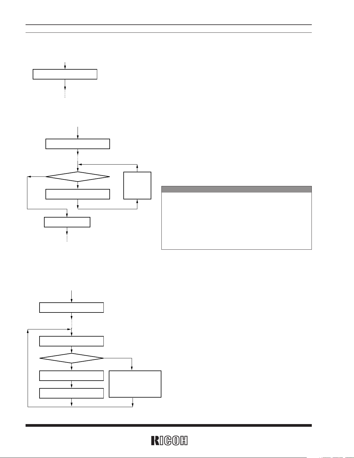
When using the XSTP bit
Ensure stable oscillation by preventing the following:
1) Condensation on the crystal oscillator
2) Instantaneous disconnection of power
3) Generation of clock noises, etc. in the crystal oscillator
4) Charge of voltage exceeding prescribed maximum ratings
to the individual pins of the IC
RS5C313
24
Start
XSTP=0?
BSY=0?
Interrupt cycle register←0h
Control register←3h, 7h
Control register←0h, 4h
Set clock and calendar
counters and interrupt cycles.
Wait or
other
operations.
Power-on
YES
No
YES
NO
*
1
*
2
*
3
*
4
*
6
*
5
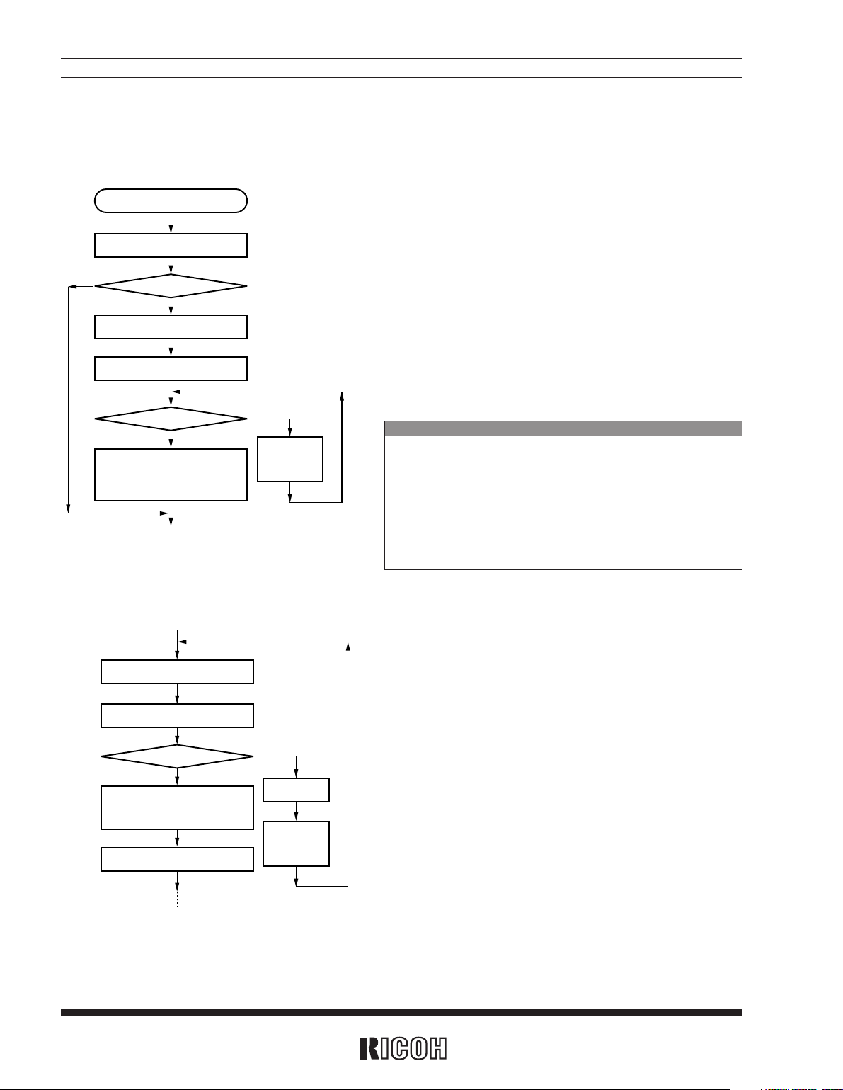
11.1 Initialization upon Power-on
11. Typical Software-based Operations
*
1) Switch the CE pin to the low level immediately after power-on.
*
2) When not making oscillation halt sensing (data validity), the XSTP bit need
not be checked.
*
3) Turn off the INTR pin, whose output is uncertain at power-on.
*
4) Write to control register 3h for 12-hour format or 7h for 24-hour format. Set
the ADJ bit to 1 for checking oscillaiton.
*
5) It takes 0.1-2 seconds to be set the BSY bit to 0 from oscillation starting upon
power-on from 0V. Provide an exit from an oscillation start loop to prepare
for oscillation failure.
*
6) Set the XSTP bit to 0 by writing data to the control register.
0h for the 12-hour time display system.
4h for the 24-hour time display system.
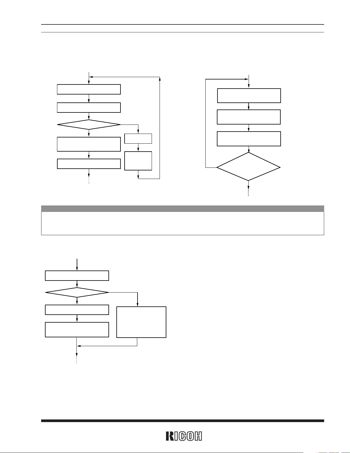
11.2 Write Operation to Clock and Calendar Counters
BSY=0?
Write to clock and
calendar counters.
CE=L
Wait or
other
operations.
CE=L
Control register←0h, 4h
CE=H
YES
NO
*
1
*
2
*
3
*
4
*
1) After switching the CE pin to the high level, hold it at the high level until any
subsequent operation requires switching it to the low level. (Note that
switching the CE pin to the low level sets the WTEN bit to 1.)
*
2) Write 0h for the 12-hour format or 4h for the 24-hour time display system.
*
3) The BSY bit is held at 1 for a maximum duration of 122.1 us.
*
4) Switch the CE pin to the low level to set the WTEN bit to 1.
During write operation to the clock and calendar counters, one 1-second
digit carry causes a 1-second increment while two 1-second digit carries
also cause only a 1-second increment, which, in turn, causes a time delay.
Page 28
RS5C313
25
11.3 Read Operation from Clock and Calendar Counters
CTFG=1?
Read from clock
calendar counter
Interrupt operation
from any other IC
Interrupt to CPU
Control register ←2h, 6h
YES
NO
*
6
*
7
*
8
*
1) After switching the CE pin to the high level, hold it at the high level until any
subsequent operation requires switching it to the low level. (Note that switching the CE pin to the low level sets the WTEN bit to 1.)
*
2) Write 0h for the 12-hour format or 4h for the 24-hour time display system.
*
3) The BSY bit is held at 1 for a maximum duration of 122.1 us.
*
4) Switch the CE pin to the low level to set the WTEN bit to 1.
During write operation to the clock and calendar counters, one 1-second digit
carry causes a 1-second increment while two 1-second digit carries also
cause only a 1-second increment, which, in turn, causes a time delay.
*
5) When needing any higher-order digits than the minute digits, replace second
digits with minute digits. (Reading LSD one of the required digits twice.)
*
6) Select the level mode as an interrupt mode by setting the CT3 bit to 1.
*
7) Write 2h for the 12-hour format or 6h for the 24-hour format.
*
8) Complete read operation within an interrupt cycle after interrupt generation
(e.g. within 1 second).
11.3-1
11.3-3
BSY=0?
CE=L
Wait or
other
operations.
CE=L
Control register ←0h, 4h
CE=H
YES
NO
*
1
*
2
*
3
*
4
Read from clock and
calendar counters.
11.3-2
Read from clock and
calendar counters.
Again read 1-second digit
of clock counter.
Two1-second
digit readings
match?
Read 1-second digit
of clock counter.
NO
YES
*
5
*
5
*
5
Read data as described in 11.3-2 or 11.3-3 when it takes (1/1024) sec or more to set the WTEN bit from 0 to 1 (CE=L),
the read operation described in 11.3-1 is prohibited as such a case.
Note
Page 29
When using the XSTP bit
Ensure stable oscillation by preventing the following:
1) Condensation on the crystal oscillator
2) Instantaneous disconnection of power
3) Generation of clock noises, etc. in the crystal oscillator
4) Charge of voltage exceeding prescribed maximum ratings
to the individual pins of the IC
RS5C313
26
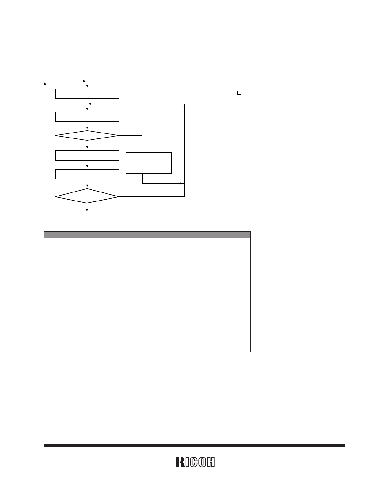
11.4 Second-digit Adjustment by ±30 seconds
Control register ←3h, 7h
*
1
*
1) Write 3h for the 12-hour format or 7h for the 24-hour format and then set the
ADJ bit to 1. (The BSY bit is held at 1 for a maximum duration of 122.1µs
after the ADJ bit is set to 1.)
11.5 Oscillation Start Judgment
XSTP=0?
Oscillation start
Wait or
other
operations
Power-on
Control register ←2h, 6h
YES
NO
*
2
*
4
*
3
*
2) The XSTP bit is set to 1 upon power-on from 0V.
*
3) It takes approximately 0.1 to 2 seconds to start oscillation.
Provide an exit from an oscillation start loop to prepare for oscillation failure.
*
4) Write 2h for the 12-hour format or 6h for the 24-hour format.
11.6 Interrupt Operation
CTFG=1?
Cyclic interrupt operation
Interrupt operation
from any other IC
Interrupt to CPU
Control register ←2h, 6h
Set interrupt cycle register
YES
NO
*
5
*
6
*
5) Set the interrupt cycle register to the level mode by setting the CT3 bit to 1.
*
6) Write 2h for the 12-hour format or 6h for the 24-hour format.
(a) Cyclic Interrupt Operation (Every 1 Second to 1 Month)
Page 30
Note
In the above typical operation, alarm time (hour and minute) is collated with
clock time by making interrupt operation a maximum of 37 times per day as
shown by the following calculation:
23(1-hour digit)+5(10-minute digit)+9(1-minute digit)=37 times
In this connection, a total current consumption increase resulting from interrupt operation can also be calculated as follows:
Assuming, for example, that interrupt operation to the CPU takes 50 ms and
consumes 10mA of current, an average current consumption increase resulting from interrupt operation can be calculated as follows: (50 ms
× 10mA× 37
times) / (60 seconds
× 60 minutes× 24 hours)=0.21µA Counting in a standard
current consumption of about 0.91µA when the RS5C313 is set to 3V, a total
current consumption can be calculated at about 1.1µA.
*
1) In this typical operation, alarm time is stored in the CPU and collated with
clock time through interrupt operation.
*
2) Initially set address h to Ch (every 1 hour) and change it in the following
sequence for every matching of clock counter readings in
Ch
→
Bh →Ah →(9h →8h)
Every Every Every (Every Every)
1 hour 10 mins. 1 min. (10 secs. 1 sec.)
In this manner, change the settings of the interrupt cycle register.
*
3) Write 2h for the 12-hour format or 6h for the 24-hour format.
*
4) Collate alarm time with clock time through interrupt operation.
Interrupt Setting
Time Digit for Collation
Ch 10-hour and 1-hour digits
Bh 10-minute digit (10-hour and 1-hour digits)
Ah 1-minute digit
(10-hour, 1-hour, and 10-minute digits)
(9h) 10-second digit
(10-hour digit to 1-minute digit)
(8h) 1-second digit
(10-hour digit to 10-second digit)
RS5C313
27
CTFG=1?
Read from clock counter
Interrupt operatin
from any other IC
Interrupt to CPU
Control register ←2h, 6h
Interrupt cycle register ← h
YES
YES
NO
Readings match?
NO
*
2
*
3
*
4
(b) Daily Time (Hour or Minute) Alarm Operation*
1
Page 31
RS5C313
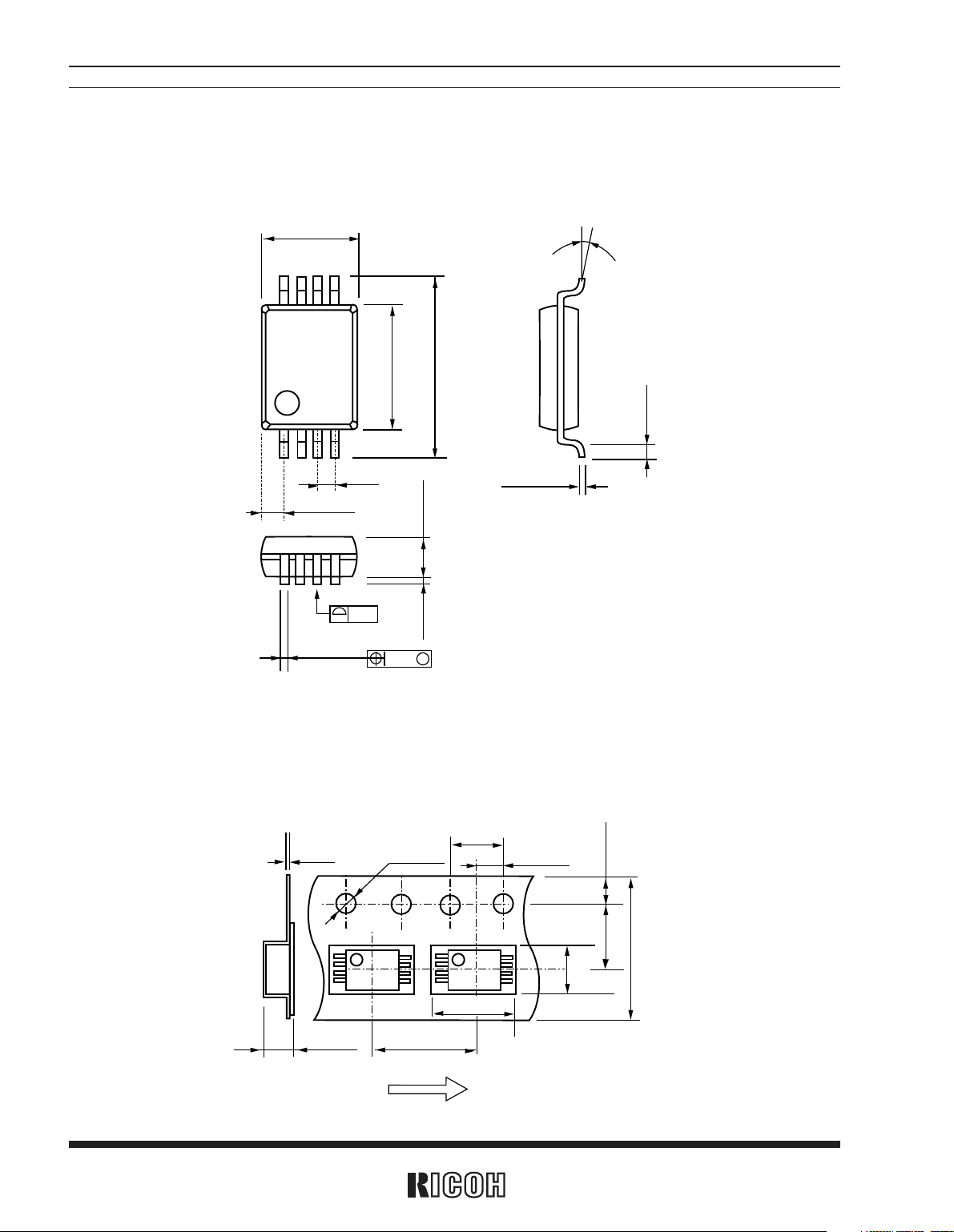
28
• 8pin SSOP (0.65mm pitch)
PACKAGE DIMENSIONS(Unit:mm)
0.15
+0.1
-
0.05
0.5±0.3
0° to 10°
0.1±0.1
0.15
0.1
M
0.22±0.1
1.15±0.1
0.775TYP.
0.65
1
4
6.4±0.3
4.4±0.2
8
5
3.5±0.3
TAPING SPECIFICATION(Unit:mm)
0.3
2.7 MAX.
4.0±0.1
2.0±0.05
8.0±0.1
1.75
±
0.1
5.5±0.05
3.9
6.7
12.0±0.3
User Direction of Feed.
ø1.5
+0.1
–0
The RS5C313 has one designated taping direction. The product designation for the taping components is
“RS5C313-E2”.
Page 32

RICOH COMPANY, LTD.
ELECTRONIC DEVICES DIVISION
HEADQUARTERS
13-1, Himemuro-cho, Ikeda City, Osaka 563-8501, JAPAN
Phone +81-727-53-6003 Fax +81-727-53-2120
YOKOHAMA OFFICE (International Sales)
3-2-3, Shin-Yokohama, Kohoku-ku, Yokohama City, Kanagawa 222-8530,
JAPAN
Phone +81-45-477-1697 Fax +81-45-477-1694 · 1695
http://www.ricoh.co.jp/LSI/english/
RICOH CORPORATION
ELECTRONIC DEVICES DIVISION
SAN JOSE OFFICE
1996 Lundy Avenue, San Jose, CA 95131, U.S.A.
Phone +1-408-944-3306 Fax +1-408-432-8375
http://www.ricoh-usa.com/semicond.htm
 Loading...