

Page 1

I2C bus SERIAL INTERFACE
REAL-TIME CLOCK ICs
RS5C372A/B
ELECTRONIC DEVICES DIVISION
NO.EA-044-9908
APPLICATION MANUAL
Page 2

NOTICE
1. The products and the product specifications described in this application manual are subject to change or discontinuation of production without notice for reasons such as improvement. Therefore, before deciding to use
the products, please refer to Ricoh sales representatives for the latest information thereon.
2. This application manual may not be copied or otherwise reproduced in whole or in part without prior written consent of Ricoh.
3. Please be sure to take any necessary formalities under relevant laws or regulations before exporting or otherwise taking out of your country the products or the technical information described herein.
4. The technical information described in this application manual shows typical characteristics of and example
application circuits for the products. The release of such information is not to be construed as a warranty of or a
grant of license under Ricoh's or any third party's intellectual property rights or any other rights.
5. The products listed in this document are intended and designed for use as general electronic components in
standard applications (office equipment, computer equipment, measuring instruments, consumer electronic
products, amusement equipment etc.). Those customers intending to use a product in an application requiring
extreme quality and reliability, for example, in a highly specific application where the failure or misoperation of
the product could result in human injury or death (aircraft, spacevehicle, nuclear reactor control system, traffic
control system, automotive and transportation equipment, combustion equipment, safety devices, life support
system etc.) should first contact us.
6. We are making our continuous effort to improve the quality and reliability of our products, but semiconductor
products are likely to fail with certain probability. In order prevent any injury to persons or damages to property
resulting from such failure, customers should be careful enough to incorporate safety measures in their design,
such as redundancy feature, fire-containment feature and fail-safe feature. We do not assume any liability or
responsibility for any loss or damage arising from misuse or inappropriate use of the products.
7. Anti-radiation design is not implemented in the products described in this application manual.
8. Please contact Ricoh sales representatives should you have any questions or comments concerning the products or the technical information.
June 1995
Page 3

RS5C372A
OUTLINE
...................................................................................................
1
FEATURES
................................................................................................
1
BLOCK DIAGRAM
.....................................................................................
2
APPLICATIONS
.........................................................................................
2
PIN CONFIGURATION
................................................................................
2
PIN DESCRIPTIONS
..................................................................................
3
ABSOLUTE MAXIMUM RATINGS
...............................................................
3
RECOMMENDED OPERATING CONDITIONS
..............................................
4
DC CHARACTERISTICS
.............................................................................
4
AC CHARACTERISTICS
.............................................................................
5
RS5C372B
OUTLINE
...................................................................................................
7
FEATURES
................................................................................................
7
BLOCK DIAGRAM
.....................................................................................
8
APPLICATIONS
.........................................................................................
8
PIN CONFIGURATION
................................................................................
8
PIN DESCRIPTIONS
..................................................................................
9
ABSOLUTE MAXIMUM RATINGS
...............................................................
9
RECOMMENDED OPERATING CONDITIONS
............................................
10
DC CHARACTERISTICS
...........................................................................
10
AC CHARACTERISTICS
...........................................................................
11
RS5C372A/B
GENERAL DESCRIPTION
.........................................................................
13
FUNCTIONAL DESCRIPTIONS
.................................................................
15
1. Allocation of Internal Addresses
..................................................................
15
2. Registers
.............................................................................................
16
RS5C372A/B
APPLICATION MANUAL
CONTENTS
Page 4

USAGES
..................................................................................................
26
1. Interfacing with the CPU
...........................................................................
26
2. Configuration of Oscillating Circuit and Time Trimming
........................................
35
3. Oscillator Halt Sensing
.............................................................................
40
4. INTRA Output and INTRB Output Pins (RS5C372A), INTR Output Pin (RS5C372B)
....
40
5. Typical Applications
.................................................................................
46
6. Typical Characteristic Measurements
............................................................
49
7. Typical Software-based Operations
...............................................................
51
PACKAGE DIMENSIONS
..............................................................................
54
TAPING SPECIFICATION
..............................................................................
54
Page 5

I2C bus SERIAL INTERFACE
REAL-TIME CLOCK IC
RS5C372A
1
OUTLINE
The RS5C372A is a CMOS type real-time clock which is connected to the CPU via 2-wires and capable of serial
transmission of clock and calendar data to the CPU.
The RS5C372A can generate various periodic interrupt clock pulses lasting for long period (one month), and
alarm interrupt can be made by days of the week, hours, and minutes by two incorporated systems. Since an oscillation circuit is driven at a constant voltage, it undergoes fluctuations of few voltage and consequently offers low current consumption (TYP. 0.5µA at 3V). It also provides an oscillator halt sensing function applicable for data validation at power-on and other occasions and 32-kHz clock output for an external micro computer. (Nch. open drain output) The product also incorporates a time trimming circuit that adjusts the clock with higher precision by adjusting
any errors in crystal oscillator frequencies based on signals from the CPU. The crystal oscillator may be selected
from 32.768kHz or 32.000kHz types. Integrated into an ultra compact and ultra thin 8 pin SSOP package, the
RS5C372A is the optimum choice for equipment requiring small sized and low power consuming products.
FEATURES
• Time keeping voltage: 1.45V to 6.0V
• Lowest supply current: 0.5µA TYP. (0.9µA MAX.) : 3V (25˚C)
(1.0µA MAX.) : 3V (–40 to +85˚C)
• Connected to the CPU via only 2-wires (I
2
C bus Interface, MAX.400kHz, address 7bit)
• A clock counter (counting hours, minutes, and seconds) and a calendar counter (counting leap years, years,
months, days, and days of the week) in BCD codes
• Interrupt to the CPU (period of one month to one second, interrupt flag, interrupt halt function) (INTRA, INTRB)
• Two systems of alarm functions (days of the week, hours, and minutes) (INTRA, INTRB)
• Oscillation halt sensing to judge internal data validity
• Clock output of 32.768kHz (32.000kHz) (output controllable via a register)
...
(Nch. open drain output)
• Second digit adjustment by ±30 seconds
• Automatic leap year recognition up to the year 2099
• 12-hour or 24-hour time display selectable
• Oscillation stabilizing capacity (C
G, CD) incorporated
• High precision time trimming circuit
• Oscillator of 32.768kHz or 32.000kHz may be used
• CMOS logic
• Package: 8pin SSOP
Note
· I2C bus is a trademark of PHILIPS ELECTRONICS N.V.
· Purchase of I
2
C components of Ricoh Company, Ltd. conveys a license under the Philips I2C Patent Rights to
use these components in an I
2
C system, provided that the system comforms to the I2C Standard Specifica-
tion as defined by Philips.
Page 6
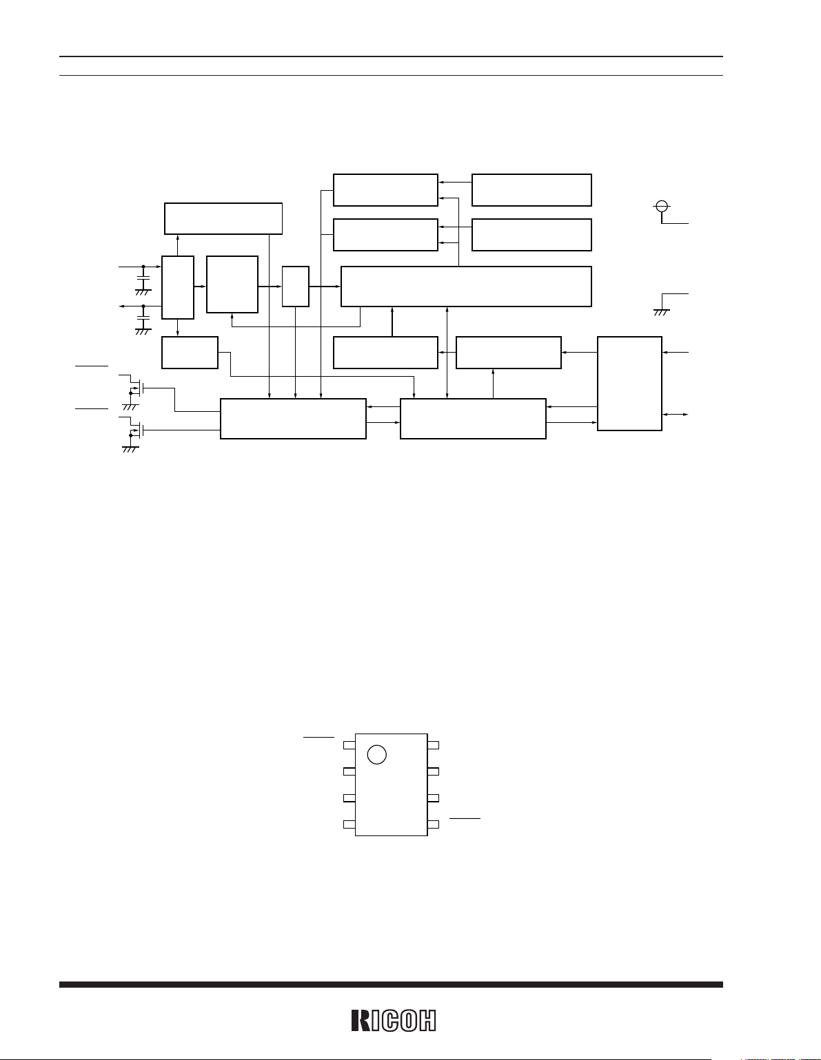
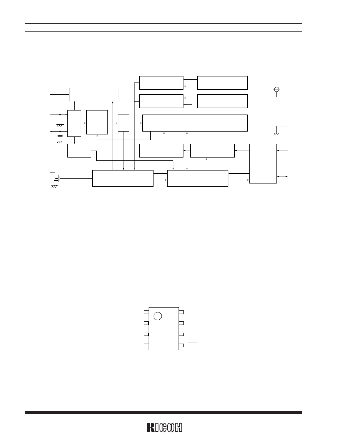
RS5C372A
2
BLOCK DIAGRAM
COMPARATOR_A
ALARM_A REGISTER
(WEEK,MIN,HOUR)
ALARM_B REGISTER
(WEEK,MIN,HOUR)
COMPARATOR_B
TIME COUNTER
(SEC,MIN,HOUR,WEEK,DAY,MONTH,YEAR)
ADDRESS
REGISTER
ADDRESS
DECODER
SHIFT REGISTERINTERRUPT CONTROL
32kHz OUTPUT
CONTROL
DIVIDER
CORREC
-TION
DIVOSC
OSCIN
OSCOUT
OSC
DETECT
I/O
CONTROL
VSS
SCL
SDA
VDD
INTRA
INTRB
PIN CONFIGURATION
• 8pin SSOP
INTRB
1
SCL
2
SDA
3
VSS
VDD
OSCIN
OSCOUT
INTRA
4
8
7
6
5
APPLICATIONS
• Communication devices (multi function phone, portable phone, PHS or pager)
• OA devices (fax, portable fax)
• Computer (desk-top and mobile PC, portable word-processor, PDA, electric note or video game)
• AV components (portable audio unit, video camera,camera, digital camera or remote controller)
• Home appliances (rice cooker, electric oven)
• Other (car navigation system, multi-function watch)
Page 7
RS5C372A
3
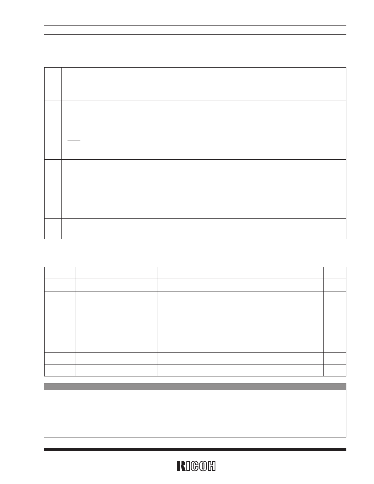
PIN DESCRIPTIONS
Pin No.
Symbol Name Description
2 SCL Serial Clock Line
This pin is used to input shift clock pulses to synchronize data input/output to and
from the SDA pin with this clock. Up to 6V beyond VDD may be input.
3 SDA Serial Data Line
This pin inputs and outputs written or read data in synchronization with shift clock
pulses from the SCL pin. Up to 6V beyond V
DD may be input. This pin functions
as an Nch open drain output.
5 INTRA Interrupt Output A
This pin outputs periodic interrupt pulses and alarm interrupt (Alarm_A, Alarm_B)
to the CPU. This pin is off when power is activated from 0V. This pin functions as
an Nch open drain output.
1 INTRB Interrupt Output B
This pin outputs 32.768kHz clock pulses (when 32.768kHz crystal is used), periodic interrupt pulses to the CPU or alarm interrupt (Alarm_B). It outputs 32.768kHz
when power source is activated from 0V. This pin functions as an Nch open drain
output.
7 OSCIN Oscillator Circuit
6
OSCOUT
Input/Output
8 VDD
Positive Power Supply Input
4 VSS
Negative Power Supply Input
These pins configure an oscillator circuit by connecting a 32.768kHz or 32.000kHz
crystal oscillator between the OSCIN–OSCOUT pins.
(Any other oscillator circuit components are built into the RS5C372A.)
The VDD pin is connected to the positive power supply and VSS to the ground.
ABSOLUTE MAXIMUM RATINGS
(Vss=0V)
Symbol Item Conditions Ratings Unit
VDD Supply Voltage –0.3 to +7.0 V
VI Input Voltage SCL, SDA –0.3 to +7.0 V
VO1 Output Voltage 1 SDA –0.3 to +7.0
V
VO2 Output Voltage 2
INTRA, INTRB
–0.3 to +12
PD Power Dissipation Topt=25˚C 300 mW
Topt Operating Temperature –40 to +85 ˚C
Tstg Storage Temperature –55 to +125 ˚C
ABSOLUTE MAXIMUM RATINGS
Absolute Maximum ratings are threshold limit values that must not be exceeded even for an instant under
any conditions. Moreover, such values for any two items must not be reached simultaneously. Operation
above these absolute maximum ratings may cause degradation or permanent damage to the device. These
are stress ratings only and do not necessarily imply functional operation below these limits.
Page 8
RS5C372A
4
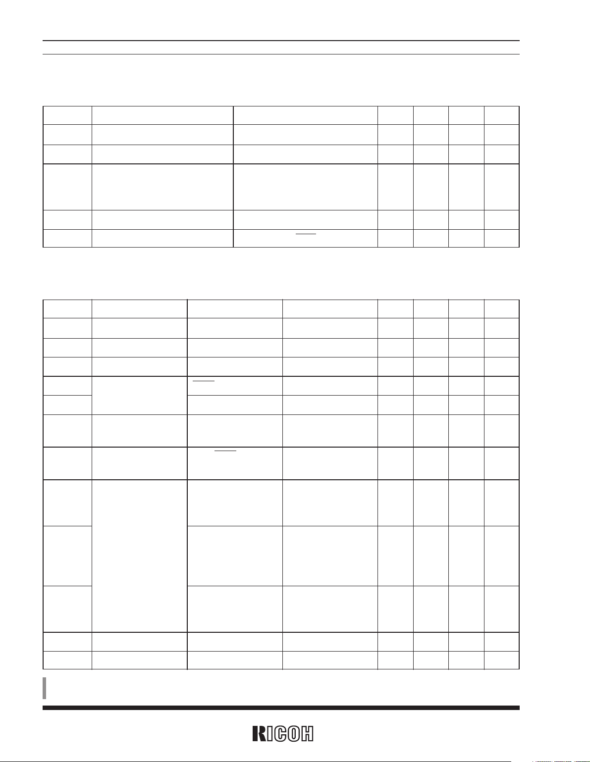
RECOMMENDED OPERATING CONDITIONS
(Vss=0V, Topt=–40 to +85˚C)
Symbol Item Conditions MIN. TYP. MAX. Unit
VDD Supply Voltage 2.0 6.0 V
VCLK Timekeeping Voltage 1.45 6.0 V
32.768
F
XT Oscillation Frequency or kHz
32.000
VPUP1 Pull-up Voltage 1 SCL, SDA 6.0 V
V
PUP2 Pull-up Voltage 2
INTRA, INTRB
10.0 V
DC CHARACTERISTICS
Unless otherwise specified: Vss=0V, VDD
=3V, Topt=–40 to +85˚C, Oscillation frequency=32.768kHz, or 32.000kHz(R1=30kΩ)
Symbol Item Pin name Conditions MIN. TYP. MAX. Unit
VIH
“H” Input Voltage SCL, SDA 0.8VDD 6.0 V
VIL “L” Input Voltage SCL, SDA –0.3 0.2VDD V
IOL1
INTRA, INTRB
V
OL1=0.4V 1 mA
IOL2 SDA VOL2=0.6V 6 mA
I
ILK Input Leakage Current SCL
V
I=6V or Vss
–1 1 µA
VDD=6V
I
OZ
Output Off State SDA, INTRA, VO=6V or Vss
–1 1 µA
Leakage Current INTRB VDD=6V
V
DD=3V, Topt=25˚C
I
DD1 VDD SCL, SDA=3V 0.5 0.9 µA
Output=OPEN
*
1
VDD=3V,
I
DD2 VDD
Topt=–40 to +85˚C
1.0 µA
SCL, SDA=3V
Output=OPEN
*
1
VDD=6V
I
DD3 VDD SCL, SDA=6V 0.8 2.0 µA
Output=OPEN
*
1
CG
Internal Oscillation Capacitance 1
OSCIN 10 pF
C
D
Internal Oscillation Capacitance 2
OSCOUT 10 pF
Output Current
Standby Current
*
1) The mode outputs no clock pulses when output is open (output off state).
For consumption current (output: no load) when 32kHz pulses are output from INTRB, see “USAGES, 6. Typical Characteristic Measurements”
Page 9
RS5C372A
5
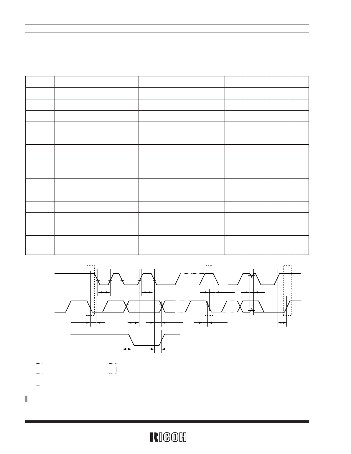
AC CHARACTERISTICS
Unless otherwise specified : VSS=0V, Topt=–40 to +85˚C, Crystal=32.768kHz or 32.000kHz
I/O conditions: V
IH=0.8×VDD, VIL=0.2×VDD, VOL=0.2×VDD, CL=50pF
Symbol Item Conditions MIN. TYP. MAX. Unit
fSCL SCL Clock Frequency 0 100 kHz
tLOW SCL Clock “L” Time 4.7 µs
tHIGH SCL Clock “H” Time 4.0 µs
tHD ; STA Start Condition Hold Time 4.0 µs
tSU ; STO Stop Condition Setup Time 4.0 µs
tSU ; STA Start Condition Setup Time 4.7 µs
tSU ; DAT Data Setup Time 250 ns
tHDH ; DAT “H” Data Hold Time 0 ns
tHDL ; DAT “L” Data Hold Time 35 ns
tPL ; DAT
SDA “L” Stable Time After Falling of SCL
2.0 µs
tPZ ; DAT
SDA off Stable Time After Falling of SCL
2.0 µs
tR
Rising Time of SCL and SDA (Input)
1000 ns
tF
Falling Time of SCL and SDA (Input)
300 ns
tSP
Spike Width that can be Removed
50 ns
with Input Filter
*
) For detailed information refer to “USAGES, 1.2 Transmission System of I2C bus.”
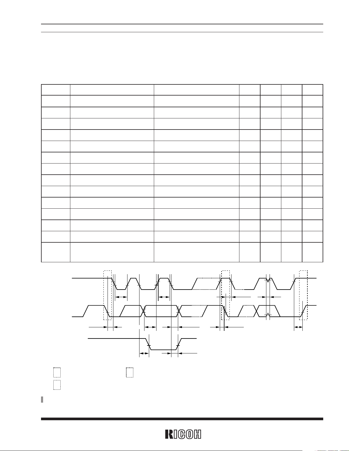
• VDD≥2.0V (supports standard mode I2C bus)
SCL
SDA(IN)
SDA(OUT)
S
S Sr P
t
LOW
tHD;STA tHDH;DAT
Start condition
tSU;DAT
tPL;DAT
Stop condition
P
tHIGH
tHDL;DAT
tPZ;DAT
tHD;STA tSP
tSU;STA
tSU;STO
Sr
Repeated start condition
Page 10

RS5C372A
6
Unless otherwise specified : VSS=0V, Topt=–40 to +85˚C, Crystal=32.768kHz or 32.000kHz
I/O conditions: V
IH=0.8×VDD, VIL=0.2×VDD, VOL=0.2×VDD, CL=50pF
Symbol Item Conditions MIN. TYP. MAX. Unit
fSCL SCL Clock Frequency 0 400 kHz
tLOW SCL Clock “L” Time 1.3 µs
tHIGH SCL Clock “H” Time 0.6 µs
tHD ; STA Start Condition Hold Time 0.6 µs
tSU ; STO Stop Condition Setup Time 0.6 µs
tSU ; STA Start Condition Setup Time 0.6 µs
tSU ; DAT Data Setup Time 100 ns
tHDH ; DAT “H” Data Hold Time 0 ns
tHDL ; DAT “L” Data Hold Time 35 ns
tPL
; DAT
SDA “L” Stable Time After Falling of SCL
0.9 µs
tPZ ; DAT
SDA Off Stable Time After Falling of SCL
0.9 µs
tR
Rising Time of SCL and SDA (Input)
300 ns
tF
Falling Time of SCL and SDA (Input)
300 ns
tSP
Spike Width that can be Removed
50 ns
with Input Filter
*
) For detailed information refer to “USAGES, 1.2 Transmission System of I2C bus.”
• VDD≥2.5V (supports fast mode I2C bus)
SCL
SDA(IN)
SDA(OUT)
S
S Sr P
t
LOW
tHD;STA tHDH;DAT
Start condition
tSU;DAT
tPL;DAT
Stop condition
P
tHIGH
tHDL;DAT
tPZ;DAT
tHD;STA tSP
tSU;STA
tSU;STO
Sr
Repeated start condition
Page 11

I2C bus SERIAL INTERFACE
REAL-TIME CLOCK IC
RS5C372B
7
OUTLINE
The RS5C372B is a CMOS type real-time clock which is connected to the CPU via 2-wires and capable of serial
transmission of clock and calendar data to the CPU.
The RS5C372B can generate various periodic interrupt clock pulses lasting for long period (one month), and
alarm interrupt can be made by days of the week, hours, and minutes by two incorporated systems. Since an oscillation circuit is driven at a constant voltage, it undergoes fluctuations of few voltage and consequently offers low current consumption (TYP. 0.5µA at 3V). It also provides an oscillator halt sensing function applicable for data validation at power-on and other occasions and 32-kHz clock output for an external micro computer. (CMOS output) The
product also incorporates a time trimming circuit that adjusts the clock with higher precision by adjusting any
errors in crystal oscillator frequencies based on signals from the CPU. The crystal oscillator may be selected from
32.768kHz or 32.000kHz types. Integrated into an ultra compact and ultra thin 8 pin SSOP package, the RS5C372B
is the optimum choice for equipment requiring small sized and low power consuming products.
FEATURES
• Time keeping voltage: 1.45V to 6.0V
• Lowest supply current: 0.5µA TYP. (0.9µA MAX.) : 3V (25˚C)
(1.0µA MAX.) : 3V (–40 to +85˚C)
• Connected to the CPU via only 2-wires (I
2
C bus Interface, MAX.400kHz, address 7bit)
• A clock counter (counting hours, minutes, and seconds) and a calendar counter (counting leap years, years,
months, days, and days of the week) in BCD codes
• Interrupt to the CPU (period of one month to one second, interrupt flag, interrupt halt function) (INTR)
• Two systems of alarm functions (days of the week, hours, and minutes) (INTR)
• Oscillation halt sensing to judge internal data validity
• Clock output of 32.768kHz (32.000kHz) (output controllable via a register)
...
(CMOS output)
• Second digit adjustment by ±30 seconds
• Automatic leap year recognition up to the year 2099
• 12-hour or 24-hour time display selectable
• Oscillation stabilizing capacity (C
G, CD) incorporated
• High precision time trimming circuit
• Oscillator of 32.768kHz or 32.000kHz may be used
• CMOS logic
• Package: 8pin SSOP
Note
· I2C bus is a trademark of PHILIPS ELECTRONICS N.V.
· Purchase of I
2
C components of Ricoh Company, Ltd. conveys a license under the Philips I2C Patent Rights to
use these components in an I
2
C system, provided that the system comforms to the I2C Standard Specifica-
tion as defined by Philips.
Page 12
RS5C372B
8
BLOCK DIAGRAM
COMPARATOR_A
ALARM_A REGISTER
(WEEK,MIN,HOUR)
ALARM_B REGISTER
(WEEK,MIN,HOUR)
COMPARATOR_B
TIME COUNTER
(SEC,MIN,HOUR,WEEK,DAY,MONTH,YEAR)
ADDRESS
REGISTER
ADDRESS
DECODER
SHIFT REGISTERINTERRUPT CONTROL
32kHz OUTPUT
CONTROL
DIVIDER
CORREC
-TION
DIVOSC
OSCIN
OSCOUT
32KOUT
OSC
DETECT
I/O
CONTROL
VSS
SCL
SDA
VDD
INTR
PIN CONFIGURATION
• 8pin SSOP
32KOUT
1
SCL
2
SDA
3
VSS
VDD
OSCIN
OSCOUT
INTR
4
8
7
6
5
APPLICATIONS
• Communication devices (multi function phone, portable phone, PHS or pager)
• OA devices (fax, portable fax)
• Computer (desk-top and mobile PC, portable word-processor, PDA, electric note or video game)
• AV components (portable audio unit, video camera,camera, digital camera or remote controller)
• Home appliances (rice cooker, electric oven)
• Other (car navigation system, multi-function watch)
Page 13
RS5C372B
9
PIN DESCRIPTIONS
Pin No.
Symbol Name Description
2 SCL Serial Clock Line
This pin is used to input shift clock pulses to synchronize data input/output to and
from the SDA pin with this clock. Up to 6V beyond VDD may be input.
3 SDA Serial Data Line
This pin inputs and outputs written or read data in synchronization with shift clock
pulses from the SCL pin. Up to 6V beyond V
DD may be input. This pin functions
as an Nch open drain output.
5 INTR Interrupt Output
This pin outputs periodic interrupt pulses and alarm interrupt (Alarm_A, Alarm_B)
to the CPU. This pin is off when power is activated from 0V. This pin functions as
an Nch open drain output.
1 32KOUT
32-kHz Clock Output
The 32KOUT pin is used to output 32.768kHz clock pulses (when 32.768kHz crystal is used). Enabled at power-on from 0volts. CMOS output. The RS5C372B can
disable 32-kHz clock output in response to a command from the host computer.
7 OSCIN Oscillator Circuit
6
OSCOUT
Input/Output
8 VDD
Positive Power Supply Input
4 VSS
Negative Power Supply Input
These pins configure an oscillator circuit by connecting a 32.768kHz or 32.000kHz
crystal oscillator between the OSCIN–OSCOUT pins.
(Any other oscillator circuit components are built into the RS5C372A.)
The VDD pin is connected to the positive power supply and VSS to the ground.
ABSOLUTE MAXIMUM RATINGS
(Vss=0V)
Symbol Item Conditions Ratings Unit
VDD Supply Voltage –0.3 to +7.0 V
VI Input Voltage SCL, SDA –0.3 to +7.0 V
Output Voltage 1 SDA –0.3 to +7.0
VO Output Voltage 2
INTR
–0.3 to +12 V
Output Voltage 3
32KOUT
–0.3 to VDD+0.3
PD Power Dissipation Topt=25˚C 300 mW
Topt Operating Temperature –40 to +85 ˚C
Tstg Storage Temperature –55 to +125 ˚C
ABSOLUTE MAXIMUM RATINGS
Absolute Maximum ratings are threshold limit values that must not be exceeded even for an instant under
any conditions. Moreover, such values for any two items must not be reached simultaneously. Operation
above these absolute maximum ratings may cause degradation or permanent damage to the device. These
are stress ratings only and do not necessarily imply functional operation below these limits.
Page 14
RS5C372B
10
RECOMMENDED OPERATING CONDITIONS
(Vss=0V, Topt=–40 to +85˚C)
Symbol Item Conditions MIN. TYP. MAX. Unit
VDD Supply Voltage 2.0 6.0 V
VCLK Timekeeping Voltage 1.45 6.0 V
32.768
F
XT Oscillation Frequency or kHz
32.000
VPUP1 Pull-up Voltage 1 SCL, SDA 6.0 V
V
PUP2 Pull-up Voltage 2
INTR
10.0 V
DC CHARACTERISTICS
Unless otherwise specified: Vss=0V, VDD
=3V, Topt=–40 to +85˚C, Oscillation frequency=32.768kHz, or 32.000kHz(R1=30kΩ)
Symbol Item Pin name Conditions MIN. TYP. MAX. Unit
VIH
“H” Input Voltage SCL, SDA 0.8VDD 6.0 V
VIL “L” Input Voltage SCL, SDA –0.3 0.2VDD V
IOH “H” Output Current 32KOUT VOH=VDD–0.5V –0.5 mA
IOL1
INTR, 32KOUT
V
OL1=0.4V 1 mA
IOL2 SDA VOL2=0.6V 6 mA
I
ILK Input Leakage Current SCL
V
I=6V or Vss
–1 1 µA
VDD=6V
I
OZ
Output Off State SDA, INTR VO=6V or Vss
–1 1 µA
Leakage Current 32KOUT VDD=6V
V
DD=3V, Topt=25˚C
I
DD1 VDD SCL, SDA=3V 0.5 0.9 µA
Output=OPEN
*
1
VDD=3V,
I
DD2 VDD
Topt=–40 to +85˚C
1.0 µA
SCL, SDA=3V
Output=OPEN
*
1
VDD=6V
I
DD3 VDD SCL, SDA=6V 0.8 2.0 µA
Output=Open
*
1
CG
Internal Oscillation Capacitance 1
OSCIN 10 pF
C
D
Internal Oscillation Capacitance 2
OSCOUT 10 pF
“L” Output Current
Standby Current
*
1) The mode outputs no clock pulses when output is open (output off state).
For consumption current (output: no load) when 32kHz pulses are output from 32KOUT, see “USAGES, 6. Typical Characteristic Measurements”
Page 15

RS5C372B
11
AC CHARACTERISTICS
Unless otherwise specified : VSS=0V, Topt=–40 to +85˚C, Crystal=32.768kHz or 32.000kHz
I/O conditions: V
IH=0.8×VDD, VIL=0.2×VDD, VOL=0.2×VDD, CL=50pF
Symbol Item Conditions MIN. TYP. MAX. Unit
fSCL SCL Clock Frequency 0 100 kHz
tLOW SCL Clock “L” Time 4.7 µs
tHIGH SCL Clock “H” Time 4.0 µs
tHD ; STA Start Condition Hold Time 4.0 µs
tSU ; STO Stop Condition Hetup Time 4.0 µs
tSU ; STA Start Condition Setup Time 4.7 µs
tSU ; DAT Data Setup Time 250 ns
tHDH ; DAT “H” Data Hold Time 0 ns
tHDL ; DAT “L” Data Hold Time 35 ns
tPL ; DAT
SDA “L” Stable Time After Falling of SCL
2.0 µs
tPZ ; DAT
SDA Off Stable Time After Falling of SCL
2.0 µs
tR
Rising Time of SCL and SDA (Input)
1000 ns
tF
Falling Time of SCL and SDA (Input)
300 ns
tSP
Spike Width that can be Removed
50 ns
with Input Filter
*
) For detailed information refer to “USAGES, 1.2 Transmission System of I2C bus.”
• VDD≥2.0V (supports standard mode I2C bus)
SCL
SDA(IN)
SDA(OUT)
S
S Sr P
t
LOW
tHD;STA tHDH;DAT
Start condition
tSU;DAT
tPL;DAT
Stop condition
P
tHIGH
tHDL;DAT
tPZ;DAT
tHD;STA tSP
tSU;STA
tSU;STO
Sr
Repeated start condition
Page 16
RS5C372B
12
Unless otherwise specified : VSS=0V, Topt=–40 to +85˚C, Crystal=32.768kHz or 32.000kHz
I/O conditions: V
IH=0.8×VDD, VIL=0.2×VDD, VOL=0.2×VDD, CL=50pF
Symbol Item Conditions MIN. TYP. MAX. Unit
fSCL SCL Clock Frequency 0 400 kHz
tLOW SCL Clock “L” Time 1.3 µs
tHIGH SCL Clock “H” Time 0.6 µs
tHD ; STA Start Condition Hold Time 0.6 µs
tSU ; STO Stop Condition Setup Time 0.6 µs
tSU ; STA Start Condition Setup Time 0.6 µs
tSU ; DAT Data Setup Time 100 ns
tHDH ; DAT “H” Data Hold Time 0 ns
tHDL ; DAT “L” Data Hold Time 35 ns
tPL
; DAT
SDA “L” Stable Time After Falling of SCL
0.9 µs
tPZ ; DAT
SDA Off Stable Time After Falling of SCL
0.9 µs
tR
Rising Time of SCL and SDA (Input)
300 ns
tF
Falling Time of SCL and SDA (Input)
300 ns
tSP
Spike Width that can be Removed
50 ns
with Input Filter
*
) For detailed information refer to “USAGES, 1.2 Transmission System of I2C bus.”
• VDD≥2.5V (supports fast mode I2C bus)
SCL
SDA(IN)
SDA(OUT)
S
S Sr P
t
LOW
tHD;STA tHDH;DAT
Start condition
tSU;DAT
tPL;DAT
Stop condition
P
tHIGH
tHDL;DAT
tPZ;DAT
tHD;STA tSP
tSU;STA
tSU;STO
Sr
Repeated start condition
Page 17

RS5C372A/B
13
GENERAL DESCRIPTION
1. Interfacing with the CPU
The RS5C372A/B read /write data over I2C bus interface via 2-wires: SDA (data) and SCL (clock). Since the output
of the I/O pin of SDA is open drain, data interfacing with a CPU with different supply voltage is possible by applying
pull-up resistor on the circuit board. The maximum clock frequency of 400kHz of SCL enables data transfer in I
2
C
bus fast mode.
2. Clock function
The clock function of the RS5C372A/B allows write/read data from lower two digits of the dominical year to seconds to and from the CPU. When lower two digits of the dominical year are multiples of 4, the year is recognized as
a leap year automatically. Up to the year 2099 leap years will be automatically recognized.
3. Alarm function
˙
RS5C372A
The RS5C372A has an alarm function that outputs an interrupt signal from INTRA or INTRB output pins to the CPU
when the day of the week, hour or minute corresponds to the setting. These two systems of alarms (Alarm_A,
Alarm_B), each may output interrupt signal separately at a specified time. The alarm may be selectable between on
and off for each day of the week, thus allowing outputting alarm everyday or on a specific day of the week.
The Alarm_A is output from the INTRA pin while the Alarm_B is output from either the INTRA or the INTRB pins.
Polling is possible separately for each alarm function.
˙
RS5C372B
The RS5C372B has an alarm function that outputs an interrupt signal from INTR output pin to the CPU when the
day of the week, hour or minute corresponds to the setting. These two systems of alarms (Alarm_A, Alarm_B),
each may output interrupt signal separately at a specified time. The alarm may be selectable between on and off for
each day of the week, thus allowing outputting alarm everyday or on a specific day of the week.
Polling is possible separately for each alarm function.
4. High precision time trimming function
The RS5C372A/B have an internal oscillation circuit capacitance CG and CD so that an oscillation circuit may be configured simply by externally connecting a crystal. Either 32.768kHz or 32.000kHz may be selected as a crystal oscillator by setting the internal register appropriately. The RS5C372A/B incorporate a time trimming circuit that
adjusts gain or loss of the clock from the CPU up to approx. ±189ppm (±194ppm when 32.000kHz crystal is used) by
approximately 3ppm steps to correct discrepancy in oscillation frequency. (Error after correction: ±1.5ppm: 25˚C)
Thus by adjusting frequencies for each system,
· Clock display is possible at much higher precision than conventional real-time clock while using a crystal with
broader fluctuation in precision.
· Even seasonal frequency fluctuation may be corrected by adjusting seasonal clock error.
*
) The year 2000 is a leap year while the year 2100 is not.
Page 18

RS5C372A/B
14
· For those systems that have temperature detection precision of clock function may be increased by correcting
clock error according to temperature fluctuations.
5. Oscillation halt sensing
The oscillation halt sensing function uses a register to store oscillation halt information. This function may be used
to determine if the RS5C372A/B supply power has been booted from 0V and if it has been backed up. This function
is useful for determining if clock data is valid or invalid.
6. Periodic interrupt
˙
RS5C372A
The RS5C372A can output periodic interrupt pulses in addition to alarm function from the INTRA and INTRB pins.
This frequency may be selected from 2Hz (every 0.5 seconds), 1Hz (every second), 1/60Hz (every minute),
1/3600Hz (every hour) and monthly (1st of month).
Output wave form for periodic interrupt may be selected from regular pulse waveform (2Hz and 1Hz) and waveforms (every second, every minute, every hour and every month) that are appropriate for CPU level interrupt. Outputs may be selected either INTRA or INTRB. The RS5C372A/B has polling function that monitors pin status in the
register.
˙
RS5C372B
The RS5C372B can output periodic interrupt pulses in addition to alarm function from the INTR pin. This frequency
may be selected from 2Hz (every 0.5 seconds), 1Hz (every second), 1/60Hz (every minute), 1/3600Hz (every hour)
and monthly (1st of month).
Output wave form for periodic interrupt may be selected from regular pulse waveform (2Hz and 1Hz) and waveforms (every second, every minute, every hour and every month) that are appropriate for CPU level interrupt. Periodic Interrupt outputs from INTR. The RS5C372B has polling function that monitors pin status in the register.
7. 32-kHz clock output
˙
RS5C372A
The RS5C372A may output oscillation frequency from the INTRB pin. This clock output is set for output by default,
which is set to on or off by setting the register.
˙
RS5C372B
The RS5C372B may output oscillation frequency from the 32KOUT pin. This clock output is set for output by
default, which is set to on or off by setting the register. The 32KOUT pin is CMOS push-pull output terminal.
Note
The year-digit counter of RS5C372A/B counts only lower two digits of a year and no counter is supplied for upper two
digits. When you are going to use this product in a system that must cope with “2000 year problem” which shall be
corrected by software.
Page 19

RS5C372A/B
15
FUNCTIONAL DESCRIPTIONS
1. Allocation of Internal Addresses
Internal address
Contents
Data*
1
A3 A2 A1 A0 D7 D6 D5 D4 D3 D2 D1 D0
0 0 0 0 0 Second Counter —*
2
S40 S20 S10 S8 S4 S2 S1
1 0 0 0 1 Minute Counter — M40 M20 M10 M8 M4 M2 M1
2 0 0 1 0 Hour Counter — —
H
20
H10 H8 H4 H2 H1
P/A
3 0 0 1 1 Day of the Week Counter — — — — — W4 W2 W1
4 0 1 0 0 Day Counter — — D20 D10 D8 D4 D2 D1
5 0 1 0 1 Month Counter — — — MO10 MO8 MO4 MO2 MO1
6 0 1 1 0 Year Counter Y80 Y40 Y20 Y10 Y8 Y4 Y2 Y1
7 0 1 1 1 Time Trimming Register
XSL
F6 F5 F4 F3 F2 F1 F0
8 1 0 0 0 Alarm_A (Minute Register) — AM40 AM20 AM10 AM8 AM4 AM2 AM1
9 1 0 0 1 Alarm_A (Hour Register) — —
AH
20
AH10 AH8 AH4 AH2 AH1
AP/A
A 1 0 1 0
Alarm_A (Day of the Week Register)
— AW6 AW5 AW4 AW3 AW2 AW1 AW0
B 1 0 1 1 Alarm_B (Minute Register) — BM40 BM20 BM10 BM8 BM4 BM2 BM1
C 1 1 0 0 Alarm_B (Hour Register) — —
BH
20
BH10 BH8 BH4 BH2 BH1
BP/A
D 1 1 0 1
Alarm_B (Day of the Week Register)
— BW6 BW5 BW4 BW3 BW2 BW1 BW0
E 1 1 1 0 Control Register 1 AALE BALE SL2
*
5
SL1
*
5
TEST CT2 CT1 CT0
F 1 1 1 1 Control Register 2 — — 12/24
ADJ
*
3
CLEN CTFG AAFG BAFG
XSTP
*
4
*
1) All the listed data can be read and written except for ADJ/XSTP.
*
2) The “–” mark indicates data which can be read only and set to “0” when read.
*
3) The ADJ/XSTP bit of the control register2 is set to ADJ for write and XSTP for read operation. The XSTP bit is set to “0” by writing data into the control register2 for normal oscillation.
*
4) When XSTP is set to “1”, the XSL, F6 to F0, CT2 to CT0, AALE, BALE, SL2, SL1, CLEN and TEST bits are reset to “0”.
*
5) SL1 and SL2 apply to the RS5C372A. For the RS5C372B, these bits must be filled with “0”.
Page 20

RS5C372A/B
16
2. Registers
2.1 Control Register 1 (at internal address Eh)
D7 D6 D5 D4 D3 D2 D1 D0
AALE BALE SL2
*
2
SL1
*
2
TEST CT2 CT1 CT0
AALE BALE SL2
*
2
SL1
*
2
TEST CT2 CT1 CT0
0 0 0 0 0 0 0 0
(For write operation)
(For read operation)
Default*
*
1) The default means read value when XSTP bit is set to “1” by starting up from 0V, or supply voltage drop, etc.
*
2) SL1 andSL2 apply to the RS5C372A. For the RS5C372B, these bits must be filled with “0”.
2.1-1 AALE, BALE
Alarm_A, Alarm_B enable bits
AALE, BALE Description
0 Alarm_A (Alarm_B) Correspondence action invalid
1 Alarm_A (Alarm_B) Correspondence action valid
2.1-2 SL2, SL1 (RS5C372A only)
(Default)
Interrupt output select bits
SL2 SL1 Description
0 0
Outputs Alarm_A, Alarm_B, INT to the INTRA. Outputs 32k clock pulses to the INTRB.
0 1
Outputs Alarm_A, INT to the INTRA. Outputs 32k clock pulses, Alarm_B to the INTRB.
1 0
Outputs Alarm_A, Alarm_B to the INTRA. Outputs 32k clock pulses, INT to the INTRB.
1 1
Outputs Alarm_A to the INTRA. Outputs 32k clock pulses, Alarm_B, INT to the INTRB.
By setting SL1 and SL2 bits, two alarm pulses (Alarm_A and alarm_B), periodic interrupt output (INT), 32k clock
pulses may be output to the INTRA or INTRB pins selectively.
(Default)
2.1-3 TEST
Test bit
TEST Description
0 Ordinary operation mode
1 Test mode
(Default)
The test bit is used for IC test. Set the TEST bit to 0 in ordinary operation.
Page 21

RS5C372A/B
17
2.1-4 CT2, CT1, CT0
Periodic interrupt cycle select bit
CT2 CT1 CT0
Description
Wave Form Mode
Cycle and Falling Timing
0 0 0 — off (“H”)
0 0 1 — Fixed at “L”
0 1 0 Pulse Mode 2Hz (Duty50%)
0 1 1 Pulse Mode 1Hz (Duty50%)
1 0 0 Level Mode Every second (synchronized with second count up)
1 0 1 Level Mode Every minute (00 second of every minute)
1 1 0 Level Mode Every hour (00 minute(s) 00 second(s) of every hour)
1 1 1 Level Mode
Every month (the 1st day 00 A.M. 00 minute(s) 00 second(s) of every month)
1) Pulse mode : Outputs 2Hz, 1Hz clock pulses. For relationships with counting up of seconds see the diagram
below.
(Default)
*
) When 32.000kHz crystal is used,
In the 2Hz clock pulse mode, 0.496s clock pulses and 0.504s clock pulse are output alternately.
Duty cycle for 1Hz clock pulses becomes 50.4% (“L” duration is 0.496s while “H” duration is 0.504s).
2) Level mode : One second, one minute or one month may be selected for an interrupt cycle. Counting up of seconds is matched with falling edge of interrupt output.
3) When the time trimming circuit is used, periodic interrupt cycle changes every 20 seconds.
Pulse mode : “L” duration of output pulses may change in the maximum range of ±3.784ms (±3.875ms when
32.000kHz crystal is used.)
For example, Duty will be 50±0.3784% (or 50±0.3875% when 32.000kHz crystal is used) at 1Hz.
Level mode : Frequency in one second may change in the maximum range of ±3.784ms (±3.875ms when
32.000kHz crystal is used.)
Relation Between Mode Waveforms and CTFG Bit
• Pulse mode
Approx. 92µs (32.768kHz crystal is used)
Approx. 94µs (32.000kHz crystal is used)
CTFG bit
(Counting up of seconds)
INTRA or INTRB pins
(INTR pin for the RS5C372B)
*
) Since counting up of seconds and the falling edge has a time lag of approx. 92µs (at 32.768kHz) (approx. 94µs when 32.000kHz crystal is used), time
with apparently approx. one second of delay from time of the real-time clock may be read when time is read in synchronization with the falling edge of
output.
Page 22

RS5C372A/B
18
• Level mode
Write 0 to CTFG
(Second count-up)
Write 0 to CTFG
CTFG bit
(Second count-up) (Second count-up)
INTRA or INTRB pins
(INTR pin for the RS5C372B)
2.2 Control Register 2 (at internal address Fh)
D7 D6 D5 D4 D3 D2 D1 D0
— — 12/24 ADJ CLEN CTFG AAFG BAFG
0 0 12/24 XSTP CLEN CTFG AAFG BAFG
0 0 Undefined 1 0 0 0 0
(For write operation)
(For read operation)
Default*
*
) The default means read value when XSTP bit is set to “1” by starting up from 0V, or supply voltage drop, etc.
2.2-1 12/24
12/24-hour Time Display System Selection bit
12/24 Description
0 12-hour time display system (separate for mornings and afternoons)
1 24-hour time display system
Being set this bit at “0” indicates 12-hour display system while “1” indicates 24-hour system.
Time Display Digit Table
24-hour time display system 12-hour time display system 24-hour time display system 12-hour time display system
00 12 (AM12) 12 32 (PM12)
01 01 (AM 1) 13 21 (PM 1)
02 02 (AM 2) 14 22 (PM 2)
03 03 (AM 3) 15 23 (PM 3)
04 04 (AM 4) 16 24 (PM 4)
05 05 (AM 5) 17 25 (PM 5)
06 06 (AM 6) 18 26 (PM 6)
07 07 (AM 7) 19 27 (PM 7)
08 08 (AM 8) 20 28 (PM 8)
09 09 (AM 9) 21 29 (PM 9)
10 10 (AM10) 22 30 (PM10)
11 11 (AM11) 23 31 (PM11)
*
) Either the 12-hour or 24-hour time display system should be selected before writing time data.
Page 23

RS5C372A/B
19
2.2-2 ADJ
±30 Second Adjust Bit
ADJ Description
0 Ordinary operation
1 Second digit adjustment
· The following operations are performed by setting the second ADJ bit to 1.
1) For second digits ranging from “00” to “29” seconds:
Time counters smaller than seconds are reset and second digits are set to “00”.
2) For second digits ranging from “30” to “59” seconds:
Time counters smaller than seconds are reset and second digits are set to “00”. Minute digits are incremented
by 1.
· Second digits are adjusted within 122µs (within 125µs: when 32.000kHz crystal is used) from writing operation to
ADJ.
· The ADJ bit is for write only and allows no read operation.
2.2-3 XSTP
Oscillator Halt Sensing Bit
XSTP Description
0 Ordinary oscillation
1 Oscillator halt sensing
(Default)
The XSTP bit senses the oscillator halt.
· When oscillation is halted after initial power on from 0V or drop in supply voltage the bit is set to “1” and which
remains to be “1” after it is restarted. This bit may be used to judge validity of clock and calendar count data after
power on or supply voltage drop.
· When this bit is set to “1”, XSL, F
6 to F0, CT2, CT1, CT0, AALE, BALE, SL2, SL1, CLEN and TEST bits are reset to
“0”. INTRA(INTR)*will stop output and the INTRB(32KOUT)*will output 32kHz clock pulses.
· The XSTP bit is set to “0” by setting the control register 2 (address Fh) during ordinary oscillation.
32-kHz Clock Output Bit
CLEN Description
0 32-kHz clock output enabled
1 32-kHz clock output disabled
(Default)
By setting this bit to “0”, output of clock pulses of the same frequency as the crystal oscillator is enabled.
2.2-4 CLEN
*
) INTRA and INTRB for the RS5C372A, INTR and 32KOUT for the RS5C372B.
Page 24

RS5C372A/B
20
2.2-5 CTFG
Periodic Interrupt Flag Bit
CTFG Description
0 Periodic interrupt output=OFF (“H”)
1 Periodic interrupt output=ON (“L”)
(Default)
This bit is set to “1” when periodic interrupt pulses are output (INTRA or INTRB=“L”) *1.
The CTFG bit may be set only to “0” in the interrupt level mode. Setting this bit to “0” sets either the INTRA or the
INTRB to OFF (“H”)
*
2
.
When this bit is set to “1” nothing happens.
Alarm_A (Alarm_B) Flag Bit
AAFG, BAFG Description
0 Unmatched alarm register with clock counter
1 Matched alarm register with clock counter
(Default)
· The alarm interruption is enabled only when the AALE, BALE bits are set to “1”. This bit turns to “1” when
matched time is sensed for each alarm.
· The AAFG, BAFG bit may be set only to “0”. Setting this bit to “0” sets either the INTRA or the INTRB to the OFF
“H”. When this bit is set to “1” nothing happens.
· When the AALE, BALE bit is set to “0”, alarm operation is disabled and “0” is read from the AAFG, BAFG bit.
Output Relationships Between the ALFG Bit and INTRA or INTRB(INTR for the RS5C372B
)
Setting of the AAFG
(BAFG) bit to 0
(Matched alarm time)
Setting of the AAFG
(BAFG) bit to 0
AAFG (BAFG) bit
(Matched alarm time) (Matched alarm time)
INTRA or INTRB pins
(INTR pin for the RS5C372B)
*
1) INTR=“L” for the RS5C372B.
*
2) INTR=OFF (“H”) for the RS5C372B.
2.2-6 AAFG, BAFG
*
) INTR to the OFF (“H” ) for the RS5C372B.
Page 25

RS5C372A/B
21
2.3 Clock Counter (at internal address 0-2h)
· Time digit display (in BCD code)
Second digits : Range from 00 to 59 and carried to minute digits when incremented from 59 to 00.
Minute digits : Range from 00 to 59 and carried to hour digits when incremented from 59 to 00.
Hour digits : See descriptions on the 12/24 bit (Section 2.2-1).
Carried to day and day-of-the-week digits when incremented from 11 p.m. to 12 a.m. or 23 to 00.
· Any registered imaginary time should be replaced with correct time as carrying to such registered imaginary time
digits from lower-order ones cause the clock counter malfunction.
2.3-1 Second digit register (at internal address 0h)
D7 D6 D5 D4 D3 D2 D1 D0
— S40 S20 S10 S8 S4 S2 S1
0 S40 S20 S10 S8 S4 S2 S1
0 Undefined Undefined Undefined Undefined Undefined Undefined Undefined
(For write operation)
(For read operation)
Default*
2.3-2 Minute digit register (at internal address 1h)
D7 D6 D5 D4 D3 D2 D1 D0
— M40 M20 M10 M8 M4 M2 M1
0 M
40 M20 M10 M8 M4 M2 M1
0 Undefined Undefined Undefined Undefined Undefined Undefined Undefined
(For write operation)
(For read operation)
Default*
2.3-3 Hour digit register (at internal address 2h)
D7 D6 D5 D4 D3 D2 D1 D0
— — P/A or H20 H10 H8 H4 H2 H1
0 0 P/A or H20 H10 H8 H4 H2 H1
0 0 Undefined Undefined Undefined Undefined Undefined Undefined
(For write operation)
(For read operation)
Default*
*
) The default means read value when XSTP bit is set to “1” by starting up from 0V, or supply voltage drop, etc.
Page 26

RS5C372A/B
22
2.4 Day-of-the-week Counter (at internal address 3h)
D7 D6 D5 D4 D3 D2 D1 D0
— — — — — W4 W2 W1
0 0 0 0 0 W4 W2 W1
0 0 0 0 0 Undefined Undefined Undefined
(For write operation)
(For read operation)
Default*
*
) The default means read value when XSTP bit is set to “1” by starting up from 0V, or supply voltage drop, etc.
· Day-of-the-week digits are incremented by 1 when carried to 1-day digits.
· Day-of-the-week digits display (incremented in septimal notation):
(W
4, W2, W1)=(0,0,0)→(0,0,1)→
....
→(1,1,0)→(0,0,0)
· The relation between days of the week and day-of-the-week digits is user changeable (e.g. Sunday=0,0,0).
· The (W
4, W
2, W1) should not be set to (1, 1, 1).
2.5 Calendar Counter (at internal address 4 to 6h)
· The automatic calendar function provides the following calendar digit displays in BCD code.
Day digits : Range from 1 to 31 (for January, March, May, July, August, October, and December).
Range from 1 to 30 (for April, June, September, and November).
Range from 1 to 29 (for February in leap years).
Range from 1 to 28 (for February in ordinary years).
Carried to month digits when cycled to 1.
Month digits : Range from 1 to 12 and carried to year digits when cycled to 1.
Year digits : Range from 00 to 99 and 00, 04, 08,..., 92, and 96 are counted as leap years.
· Any registered imaginary time should be replaced with correct time as carrying to such registered imaginary time
digits from lower-order ones cause the clock counter malfunction.
2.5-1 Day digit register (at internal address 4h)
D7 D6 D5 D4 D3 D2 D1 D0
— — D20 D10 D8 D4 D2 D1
0 0 D20 D10 D8 D4 D2 D1
0 0 Undefined Undefined Undefined Undefined Undefined Undefined
(For write operation)
(For read operation)
Default*
2.5-2 Month digit register (at internal address 5h)
D7 D6 D5 D4 D3 D2 D1 D0
— — — MO10 MO8 MO4 MO2 MO1
0 0 0 MO10 MO8 MO4 MO2 MO1
0 0 0 Undefined Undefined Undefined Undefined Undefined
(For write operation)
(For read operation)
Default*
Page 27

RS5C372A/B
23
2.5-3 Year digit register (at internal address 6h)
D7 D6 D5 D4 D3 D2 D1 D0
Y80 Y40 Y20 Y10 Y8 Y4 Y2 Y1
Y80 Y40 Y20 Y10 Y8 Y4 Y2 Y1
Undefined Undefined Undefined Undefined Undefined Undefined Undefined Undefined
(For write operation)
(For read operation)
Default*
2.6 Time Trimming Register (at internal address 7h)
D7 D6 D5 D4 D3 D2 D1 D0
XSL
F
6 F5 F4 F3 F2 F1 F0
XSL
F
6 F5 F4 F3 F2 F1 F0
0 0 0 0 0 0 0 0
(For write operation)
(For read operation)
Default*
*
) The default means read value when XSTP bit is set to “1” by starting up from 0V, or supply voltage drop, etc.
2.6-1 XSL bit
The XSL bit is used to select a crystal oscillator.
Set the XSL to “0” (default) to use 32.768kHz.
Set the XSL to “1” to use 32.000kHz.
2.6-2 F6 to F0
The time trimming circuit adjust one second count based on this register readings when second digit is 00, 20, or 40
seconds. Normally, counting up to seconds is made once per 32,768 of clock pulse (or 32,000 when 32.000kHz crystal is used) generated by the oscillator. Setting data to this register activates the time trimming circuit.
Register counts will be incremented as ((F
5, F4, F3, F2, F1, F0)–1)×2 when F6 is set to “0”.
Register counts will be decremented as ((F
5, F4, F3, F2, F1, F0)+1)×2 when F6 is set to “1”.
Counts will not change when (F
6, F5, F4, F3, F2, F1, F0) are set to (
*
, 0, 0, 0, 0, 0,*).
For example, when 32.768kHz crystal is used.
When (F
6, F5, F4, F3, F2, F1, F0) are set to (0, 0, 0, 0, 1, 1, 1), counts will change as: 32,768+(7–1)×2=32,780
(clock will be delayed) when second digit is 00, 20, or 40.
When (F
6, F5, F4, F3, F2, F1, F0) are set to (0, 0, 0, 0, 0, 0, 1), counts will remain 32,768 without changing when
second digit is 00, 20, or 40.
When (F
6, F5, F4, F3, F2, F1, F0) are set to (1, 1, 1, 1, 1, 1, 0), counts will change as: 32,768+(–2)×2=32,764
(clock will be advanced) when second digit is 00, 20, or 40.
Adding 2 clock pulses every 20 seconds: 2/(32,768
×20)=3.051ppm (or 3.125ppm when 32.000kHz crystal is used),
delays the clock by approx. 3ppm. Likewise, decrementing 2 clock pulses advances the clock by 3ppm. Thus the
clock may be adjusted to the precision of ±1.5ppm. Note that the time trimming function only adjust clock timing
and oscillation frequency and 32-kHz clock output is not adjusted.
*
) The default means read value when XSTP bit is set to “1” by starting up from 0V, or supply voltage drop, etc.
Page 28

RS5C372A/B
24
2.7 Alarm_A, Alarm_B Register (Alarm_A: internal address 8 to Ah; Alarm_B: internal address B to Dh)
2.7-1 Alarm_A minute register (internal address 8h)
D7 D6 D5 D4 D3 D2 D1 D0
— AM40 AM20 AM10 AM8 AM4 AM2 AM1
0 AM40 AM20 AM10 AM8 AM4 AM2 AM1
0 Undefined Undefined Undefined Undefined Undefined Undefined Undefined
(For write operation)
(For read operation)
Default*
2.7-2 Alarm_B minute register (internal address Bh)
D7 D6 D5 D4 D3 D2 D1 D0
— BM40 BM20 BM10 BM8 BM4 BM2 BM1
0 BM40 BM20 BM10 BM8 BM4 BM2 BM1
0 Undefined Undefined Undefined Undefined Undefined Undefined Undefined
(For write operation)
(For read operation)
Default*
2.7-3 Alarm_A hour register (internal address 9h)
D7 D6 D5 D4 D3 D2 D1 D0
— — AH20, AP/A AH10 AH8 AH4 AH2 AH1
0 0 AH20, AP/A AH10 AH8 AH4 AH2 AH1
0 0 Undefined Undefined Undefined Undefined Undefined Undefined
(For write operation)
(For read operation)
Default*
2.7-4 Alarm_B hour register (internal address Ch)
D7 D6 D5 D4 D3 D2 D1 D0
— — BH20, AP/A BH10 BH8 BH4 BH2 BH1
0 0 BH20, AP/A BH10 BH8 BH4 BH2 BH1
0 0 Undefined Undefined Undefined Undefined Undefined Undefined
(For write operation)
(For read operation)
Default*
2.7-5 Alarm_A day-of-the-week register (internal address Ah)
D7 D6 D5 D4 D3 D2 D1 D0
— AW6 AW5 AW4 AW3 AW2 AW1 AW0
0 AW6 AW5 AW4 AW3 AW2 AW1 AW0
0 Undefined Undefined Undefined Undefined Undefined Undefined Undefined
(For write operation)
(For read operation)
Default*
Page 29

RS5C372A/B
25
2.7-6 Alarm_B day-of-the-week register (internal address Dh)
D7 D6 D5 D4 D3 D2 D1 D0
— BW6 BW5 BW4 BW3 BW2 BW1 BW0
0 BW6 BW5 BW4 BW3 BW2 BW1 BW0
0 Undefined Undefined Undefined Undefined Undefined Undefined Undefined
(For write operation)
(For read operation)
Default*
*
) The default means read value when XSTP bit is set to “1” by starting up from 0V, or supply voltage drop, etc.
· Alarm_A, Alarm_B hour register D5 is set to 0 for AM and 1 for PM in the 12-hour display system at AP/A.
The register D5 indicates 10 digit of hour digit in 24-hour display system at AH
20.
· To activate alarm operation, any imaginary alarm time setting should not be left to avoid unmatching.
· In hour digit display midnight is set to 12, noon is set to 32 in 12-hour display system. (See section 2.2-1)
· AW
0 to AW6 correspond to the day-of-the-week counter (W4, W2, W1) being set at (0, 0, 0) to (1, 1, 0).
· No alarm pulses are output when all of AW
0 to AW6 are set to “0”.
Example of Alarm Time Settings
Day-of-the-week 12-hour system 24-hour system
Alarm Time Settings
Sun. Mon. Tue. Wed. Thu. Fri. Sat.
10-hour
1-hour 10-min
1-min
10-hour
1-hour 10-min
1-min
AW0 AW1 AW2 AW3 AW4 AW5 AW6
00:00 AM every day 1 1 1 1 1 1 1 1 2 0 0 0 0 0 0
01:30 AM every day 1 1 1 1 1 1 1 0 1 3 0 0 1 3 0
11:59 AM every day 1 1 1 1 1 1 1 1 1 5 9 1 1 5 9
00:00 PM on
0 1 1 1 1 1 0 3 2 0 0 1 2 0 0
Monday through Friday
01:30 PM on Sunday 1 0 0 0 0 0 0 2 1 3 0 1 3 3 0
11:59 PM on Monday,
0 1 0 1 0 1 0 3 1 5 9 2 3 5 9
Wednesday, and Friday
Designation of days of the week and AW0 to AW6 in the above table is an example.
Page 30

RS5C372A/B
26
USAGES
1. Interfacing with the CPU
The RS5C372A/B employ the I2C bus system to be connected to the CPU via 2-wires. Connection and transfer system of I
2
C bus are described in the following sections.
Note
I2C bus is a trademark of PHILIPS ELECTRONICS N.V.
1.1 Connection of I2C bus
2-wires, SCL and SDA which are connected to I2C bus are used for transmit clock pulses and data respectively.
All ICs that are connected to these lines are designed that will be not be clamped when a voltage beyond supply voltage is applied to input or output pins. Open drain pins are used for output. This construction allows communication
of signals between ICs with different supply voltages by adding a pull-up resistor to each signal line as shown in the
figure below. Each IC is designed not to affect SCL and SDA signal lines when power to each of these is turned off
separately.
VDD1
V
DD2
V
DD3
V
DD4
SCL
R
P
RP
SDA
Microcontroller
RS5C372A/B
Other
Peripheral
Device
*
1) For data interface, the following conditions must be met:
V
DD4≥VDD1
V
DD4≥VDD2
V
DD4≥VDD3
*
2) When the master is one, the microcontroller is ready for
driving SCL to “H” and R
P of SCL may not be required.
Page 31

RS5C372A/B
27
Cautions on Determining RP Resistance
(1) Voltage drop at RP due to sum of input current or output current at off conditions on each IC pin connect-
ed to the I
2
C bus shall be adequately small.
(2) Rising time of each signal shall be kept short even when all capacity of the bus is driven.
(3) Current consumed in I
2
C bus is small compared to the consumption current permitted for the entire sys-
tem.
When all ICs connected to I
2
C bus are CMOS type, condition (1) may usually be ignored since input current
and off state output current is extremely small for the many CMOS type ICs.
Thus the maximum resistance of R
P may be determined based on (2) while the minimum on (3) in most cas-
es.
In actual cases a resistor may be place between the bus and input/output pins of each IC to improve noise
margins in which case the R
P minimum value may be determined by the resistance.
Consumption current in the bus to review (3) above may be expressed by the formula below:
Bus consumption current =
(Sum of input current and off state output current of all devices in stand-by mode)
×
Bus stand-by duration
Bus stand-by duration + bus operation duration
+
Supply voltage
×bus operation duration × 2
R
P resistance × 2 ×(bus stand-by duration + bus operation duration)
+ supply voltage
×bus capacity × charging/discharging times per unit time
Operation of “
× 2” in the second member denominator in the above formula is derived from assumption that
“L” duration of SDA and SCL pins are the half of bus operation duration. “
× 2” in the numerator of the same
member is because there are two pins of SDA and SCL. The third member, (charging/discharging times per
unit time) means number of transition from “H” to “L” of the signal line.
Calculation example is shown below:
Pull-up resistor (R
P)=10kΩ, Bus capacity=50pF (both for SCL and SDA), VDD=3V
In as system with sum of input current and off state output current of each pin=0.1µA, I
2
C bus is used for
10ms every second while the rest of 990ms is in the stand-by mode. In this mode number of transitions of the
SCL pin from “H” to “L” state is 100 while SDA 50, every second.
Bus consumption current =
0.1µA
×990ms
990ms + 10ms
+
3V
×10ms × 2
10kΩ
×2 × (990ms + 10ms)
+ 3V
×50pF × (100 + 50)
= 0.099µA + 3.0µA + 0.0225µA = 3.12µA
Generally, the second member of the above formula is larger enough than the first and the third members,
bus consumption current may be determined by the second member in many cases.
.
.
.
.
Page 32

RS5C372A/B
28
1.2 Transmission System of I2C bus
1.2-1 Start and stop conditions
In I2C bus, SDA must be kept at a certain state while SCL is at the “H” state as shown below during data transmission.
tHDL;DAT or tHDH;DATtSU;DAT
SDA
SCL
The SCL and SDA pins are at the “H” level when no data transmission is made. Changing the SDA from “H” to “L”
when the SCL and the SDA are “H” activates the start condition and access is started. Changing the SDA from “L”
to “H” when the SCL is “H” activates stop condition and accessing stopped. Generation of start and stop conditions
are always made by the master (see the figure below).
Stop condition
t
SU;STOtHD;STA
Start condition
SDA
SCL
1.2-2 Data transmission and its acknowledge
After start condition is entered, data is transmitted by 1byte (8bits). Any bytes of data may be serially transmitted.
The receiving side will send an acknowledge signal to the transmission side each time 8bit data is transmitted.
The acknowledge signal is sent immediately after falling to “L” of SCL8bit clock pulses of data transmission, by
releasing the SDA by the transmission side that has asserted the bus at that time and by turning the SDA to “L” by
the receiving side. When transmission of 1byte data next to preceding 1byte of data is received, the receiving side
releases the SDA pin at falling edge of the SCL9bit of clock pulses or when the receiving side switches to the transmission side it starts data transmission. When the master is the receiving side, it generates no acknowledge signal
after the last 1byte of data from the slave to tell the transmitter that data transmission has completed when the slave
side (transmission side) continues to release the SDA pin so that the master will be able to generate stop condition.
1 2 8 9
Acknowledge signalStart condition
SCL from the master
SDA from
the transmission side
SDA from
the receiving side
Page 33

RS5C372A/B
29
1.2-3 Data transmission format in I2C bus
I2C bus generates no CE signals. In place of it each device has a 7bit slave address allocated. The first 1byte is allocated to this 7bit of slave address and to the command (R/W) for which data transmission direction is designated by
the data transmission thereafter. 7bit address is sequentially transmitted from the MSB and 2 and after bytes are
read, when 8bit is “H” and write when “L”.
The slave address of the RS5C372A/B are specified at (0110010).
At the end of data transmission/receiving stop condition is generated to complete transmission. However, if start
condition is generated without generating stop condition, repeated start condition is met and transmission/receiving
data may be continued by setting the slave address again. Use this procedures when the transmission direction
needs to be changed during one transmission.
S
Master to slave
Start condition
P
Slave to master
Stop condition
Sr Repeated start condition
A A
Acknowledge signal
A
S 0 A A A P
R/W=0 (Write)(0110010)
Data is written into
the slave from the master
When data is read from
the slave immediately
after 7bit addressing
from the master
When the transmission
direction is to be changed
during transmission.
S 1 A A P
R/W=1 (Read)(0110010)
S 0 A A Sr 1
R/W=0 (Write)(0110010)
R/W=1 (Read)(0110010)
A A P
Inform read has been completed by
not generating an acknowledge signal, to the slave side.
Inform read has been completed by
not generating an acknowledge signal,
to the slave side.
A
A
Slave address
Slave address
Slave address
Slave address
Data
Data
Data
Data
Data
Data
Data
Page 34

RS5C372A/B
30
1.2-4 Data transmission write format in the RS5C372A/B
Although the I2C bus standard defines a transmission format for the slave address allocated for each IC, transmission method of address information in IC is not defined. The RS5C372A/B transmit data the internal address pointer (4bit) and the transmission format register (4bit) at the 1byte next to one which transmitted a slave address and a
write command. For write operation only one transmission format is available and (0000) is set to the transmission
format register. The 3byte transmits data to the address specified by the internal address pointer written to the
2byte. Internal address pointer settings are automatically incremented for 4byte and after. Note that when the internal address pointer is Fh, it will change to 0h on transmitting the next byte.
Example of data writing (When writing to internal address Eh to Fh)
S01 1 0 0010
1
1 1 0 0 000A A A PA
R/W=0 (Write)
Transmission of
slave address
(0110010)
Setting of
Eh to the
internal
address
pointer
Setting of
0h to the
transmission
format
register
Writing of data to the
internal address Eh.
Writing of data to the
internal address Fh.
Data
Data
S
A A
Master to slave
Start condition
Acknowledge signal
A
P
Slave to master
Stop condition
Page 35

RS5C372A/B
31
1.2-5 Data transmission read format of the RS5C372A/B
The RS5C372A/B allow the following three readout methods of data from an internal register.
1) The first method to reading data from the internal register is to specify an internal address by setting the internal
address pointer and the transmission format register described 1.2-4, generate the repeated start condition (see
section 1.2-3) to change the data transmission direction to perform reading. The internal address pointer is set to
Fh when the stop condition is met. Therefore, this method of reading allows no insertion of the stop condition
before the repeated start condition. Set 0h to the transmission format register.
Example 1 of data read (when data is read from 2h to 4h)
S01 1 0 0010
0
0 1 0 0 000A
A A A P
A 10Sr
0
0 1 0 A11
R/W=0 (Write)
Transmission of
slave address
(0110010)
Transmission of
slave address
(0110010)
Setting of
2h to the
internal
address
pointer
Setting of
0h to the
transmission
format
register
Reading of data from
the internal address 2h.
Reading of data from
the internal address 3h.
Reading of data from
the internal address 4h.
DataDataData
Repeated start condition R/W=1 (Read)
S Sr
A A
Master to slave
Slave to master
Start condition
Acknowledge signal
Repeated start condition P Stop condition
A
Page 36

RS5C372A/B
32
2) The second method to reading data from the internal register is to start reading immediately after writing to the
internal address pointer and the transmission format register. Although this method is not based on the I
2
C bus
standard in a strict sense it still effective to shorten read time to ease load to the master. Set 4h to the transmission format register when this method is used.
Example 2 of data read (when data is read from internal addresses Eh to 1h).
S01 1 0 0010
1
1 1 0 0 010A
A
S P
A A
A A P
A A
R/W=0 (Write)
Transmission of
slave address
(0110010)
Setting of
Eh to the
internal
address
pointer
Setting of
4h to the
transmission
format
register
Reading of data from
the internal address Fh.
Master to slave
Slave to master
Start condition
Acknowledge signal
Stop condition
Reading of data from
the internal address 0h.
Reading of data from
the internal address 1h.
Reading of data from
the internal address Eh
A
Data
Data Data Data
Page 37

RS5C372A/B
33
3) The third method to reading data from the internal register is to start reading immediately after writing to the
slave address and the R/W bit. Since the internal address pointer is set to Fh by default as described in 1), this
method is only effective when reading is started from the internal address Fh.
Example 3 of data read (when data is read from internal addresses Fh to 3h).
S01 1 0 1010 A
A
S P
A A
A A P
A A
R/W=1 (Read)
Transmission of
slave address
(0110010)
Reading of data from
the internal address Fh.
Reading of data from
the internal address 1h.
Master to slave
Slave to master
Start condition
Acknowledge signal
Stop condition
Reading of data from
the internal address 2h.
Reading of data from
the internal address 3h.
Reading of data from
the internal address 0h.
A
Data
Data
DataDataData
Page 38

RS5C372A/B
34
1.2-6 Data transmission under special condition
The RS5C372A/B hold the clock tentatively for duration from start condition to stop condition to avoid invalid read
or write clock on carrying clock. When clock is carried during this period, which will be adjusted within approx.
61µs from stop condition. To prevent invalid read or write clock shall be made during one transmission operation
(from start condition to stop condition). When 0.5 to 1.0 second elapses after start condition any access to the
RS5C372A/B are automatically released to release tentative hold of the clock, set Fh to the address pointer, and
access from the CPU is forced to be terminated (the same action as made stop condition is received: automatic
resume function from the I
2
C bus interface). Therefore, one access must be completed within 0.5 seconds. The
automatic resume function prevents delay in clock even if the SCL is stopped from sudden failure of the system during clock read operation.
Also a second start condition after the first condition and before the stop condition is regarded as the “repeated start
condition.” Therefore, when 0.5 to 1.0 seconds passed after the first start condition, access to the RS5C372A/B are
automatically released.
If access is tried after automatic resume function is activated, no acknowledge signal will be output for writing while
FFh will be output for reading.
Access to the Real-time Clock
1) No stop condition shall be generated until clock read/write is started and completed.
2) One cycle read/write operation shall be completed within 0.5 seconds.
The user shall always be able to access the real-time clock as long as these two conditions are met.
Bad example of reading from seconds to hours (invalid read)
(Start condition) → (Read of seconds) → (Read of minutes) → (Stop condition) → (Start condition) → (Read
of hour) → (Stop condition)
Assuming read was started at 05:59:59 P.M. and while reading seconds and minutes the time advanced to
06:00:00 P.M. At this time second digit is hold so the read as 05:59:59. Then the RS5C372A/B confirm (Stop
condition) and carry second digit being hold and the time changes to 06:00:00 P.M. Then, when the hour
digit is read, it changes to 6. The wrong results of 06:59:59 will be read.
Page 39

RS5C372A/B
35
2. Configuration of Oscillating Circuit and Time Trimming
2.1 Configuration of Oscillating Circuit
8
7
6
RS5C372A/B
R
F
RD
CD
CG
OSCIN
OSCOUT
32kHz
VDD
V
DD
A
Typical external device:
X'tal: 32.768kHz or 32.000kHz
(R
1=30kΩ TYP.)
(C
L=6pF to 8pF)
Typical values of internal devices:
R
F 15MΩ (TYP.)
R
D 60kΩ (TYP.)
C
G, CD 10pF (TYP.)
The oscillation circuit is driven at a constant voltage of about 1.2V relative to the Vss level.
Consequently, it generates a wave form having a peak-to-peak amplitude of about 1.2V on the positive side of the Vss
level.
Considerations on Crystal Oscillator
Basic characteristics of a crystal oscillator includes R1 (equivalent series resistance: ease of oscillation) and
C
L (load capacitance: rank of center frequency). R1=TYP. of 30kΩ, CL=6 to 8pF is recommended for the
RS5C372A/B. Confirm recommended values to the manufacturer of the crystal oscillator used.
Considerations in Mounting Components Surrounding Oscillating Circuit
1) Mount the crystal oscillators in the closest possible position to the IC.
2) Avoid laying any signal or power line close to the oscillation circuit (particularly in the area marked with
“← A →” in the above figure).
3) Apply the highest possible insulation resistance between the OSCIN or OSCOUT pin and the PCB.
4) Avoid using any long parallel line to wire the OSCIN and OSCOUT pin.
5) Take extreme care not to cause condensation, which leads to various problems such as oscillation halt.
Other Relevant Considerations
1) When applying an external input of clock pulses (32.768kHz or 32.000kHz) to the OSCIN pin:
DC coupling : Prohibited due to mismatching of input levels.
AC coupling : Permissible except that unpredictable results may occur in oscillator halt sensing due to
possible sensing errors caused by noises, etc.
2) Avoid using the oscillator output of the RS5C372A/B (from the OSCOUT pin) to drive any other IC for the
purpose of ensuring stable oscillation.
Page 40

RS5C372A/B
36
2.2 Measurement of Oscillation Frequency
Frequency
counter
RS5C372A/B
32.768kHz
or
32.000kHz
OSCIN
OSCOUT
VDD
V
SS
INTRB (32KOUT)
*
4
*
4
*
3
*
1) Clock pulse of 32.768kHz or 32.000kHz is output from the
INTRB output pin on powering on (XSTP is set to 1).
*
2) Use a frequency counter having at least 6 digits (7digits or
more recommended).
*
3) Pull-up the INTRB output pin to VDD for the RS5C372A.
*
4) INTRB applies to the RS5C372A, and 32KOUT applies to the
RS5C372B. The RS5C372B does not need pull-up resistor.
2.3 Oscillation Frequency Adjustment
Adjustment amount of oscillation frequency may differ dependent on how the RS5C372A/B is used or how much
clock error is permissible in the system it is installed. Use the flow chart shown below find an optimal oscillation
frequency adjustment method.
Start
32kHz
clock used?
NO
NO
NO
YES
YES
YES
YES
NO
32kHz clock output is used, but clock
frequency precision is not considered
For clock precision errors derived by adding deflection
in crystal oscillator*
1
+ deflection in IC*2 is permissible*3.
For clock precision errors derived by adding deflection
in crystal oscillator*
1
+ deflection in IC*2 is permissible*3.
(A) course
(B) course
(C) course
(D) course
*
1) In general crystal oscillators are classified by their central frequency of CL (load capacitance) and available further grouped in several ranks as ±10,
±20 and ±50ppm of fluctuations in precision.
*
2) Fluctuations in frequency due to the IC used is generally from ±5 to ±10ppm at a room temperature.
*
3) Clock precision here is at a room temperature and is subjected to change due to temperature characteristics of the crystal itself.
Page 41

RS5C372A/B
37
(A) course
Adjustment of clock is not made for IC (no adjustment) and any C
L value may be used for the crystal oscillator. Pre-
cision fluctuations of a crystal oscillator may be selected as long as clock precision allows. Obtain the central frequency as described in section 2.2 using several crystal oscillator and ICs, determine an adjustment value as
described in “2.4 Time Trimming Circuit” which shall be set to the RS5C372A/B.
(B) course
To keep clock precision within the range of (fluctuation in crys-tal oscillator + fluctuation in IC), clock shall be
adjustment is required for each IC. On adjusting procedures see “2.4 Time Trimming Circuit.” Available selection
range for the frequency precision fluctuations and C
L (load capacitance) for a crystal oscillator may be widened by
adjusting clock frequency. Obtain the central frequency as described in section 2.2 using the crystal oscillator and
IC to be used, determine if an adjustment is possible or not using the clock adjustment circuit, perform adjustment
for each IC using the clock adjustment circuit. Up to ±1.5ppm may be adjusted at a room temperature.
(C) course
In (C) and (D) courses, adjustment of 32-kHz clock output frequency as well as clock is necessary. Frequency
adjustment for the crystal oscillator is made by adjusting both of C
G and CD connected to the both ends of the oscil-
lator. Since the RS5C372A/B incorporate the C
G and CD, oscillating frequency is required using CL of the crystal
oscillator as the reference.
Generally, relation between C
L and CG or CD is as follows:
CL =
C
G × CD
+ CS CS : Board floating capacitance
C
G + CD
Although a crystal oscillator having CL value of around 6 to 8pF is recommended for the RS5C372A/B, measure
oscillation frequency as described in section 2.2 and if frequency is high (clock gains) switch to a crystal oscillator
with smaller C
L while if frequency is small (clock loses) switch to an oscillator with larger CL. Using these proce-
dures select a crystal oscillator with optimal C
L and set unadjusted value to the clock adjustment circuit. (See section
2.4, “Time Trimming Circuit”.) We recommend to consult the crystal manufacturer on compatibility of C
L values.
High oscillation frequency (clock gains) may be adjusted by externally adding C
GOUT as shown below.
8
7
6
RS5C372A/B
R
F
RD
CD
CG
OSCIN
OSCOUT
32kHz
C
GOUT
VDD
V
DD
*
1
*
1) CGOUT shall be from 0 to 15pF.
(D) course
Select a crystal oscillator as in the (C) course, then adjust clock error for each IC as in (B) course. For clock adjusting procedures, see “2.4 Time Trimming Circuit.”
Page 42

RS5C372A/B
38
2.4 Time Trimming Circuit
Using the time trimming circuit gain or lose of clock may be adjusted with high precision by changing clock pulses
for one second every 20 seconds. When adjustment with this circuit is not necessary, set (F
6, F5, F4, F3, F2, F1, F0)
to (
*
, 0, 0, 0, 0, 0,*) to disable adjustment. (*mark indicates 0 or 1.)
Adjustment amount may be calculated using the following formula.
2.4-1 When oscillation frequency*1 >target frequency*2(clock gains)
Adjustment amount*3 =
(Oscillation frequency – Target frequency + 0.1)
Oscillation frequency ×3.051 × 10
–6
= (Oscillation frequency – Target frequency) ×10 + 1
When 32.000kHz crystal oscillator is used, the same formula,
Adjustment amount =
(Oscillation frequency – Target frequency + 0.1)
Oscillation frequency ×3.125 × 10
–6
= (Oscillation frequency – Target frequency) ×10 + 1
is used.
*
1) Oscillation frequency : Clock frequency output from the INTRB (32KOUT for the RS5C372B) pin as in “2.2 Oscillation Frequency Measurement” at a
room temperature.
*
2) Target frequency : A frequency to be adjusted to.
Since temperature characteristics of a 32.768kHz crystal oscillator are such that it will generally generates the highest frequency at a room temperature, we recommend to set the target frequency to approx. 32768.00Hz to 32768.10Hz (+3.05ppm
to 32768Hz).
We also recommend setting of approx. 32000.00Hz to 32000.10Hz (3.125ppm to 32000Hz) also for the 32.000kHz crystal.
Note that this value may differ based on the environment or place where the device will be used.
*
3) Adjustment amount : A value to be set finally to F6 to F0 bits. This value is expressed in 7bit binary digits with sign bit (two's compliment).
2.4-2 When oscillation frequency=target frequency (no clock gain or loss)
Set the adjustment value to 0 or +1, or –64 or –63 to disable adjustment.
2.4-3 When oscillation frequency<target frequency (clock loses)
Adjustment amount =
(Oscillation frequency – Target frequency)
Oscillation frequency
×3.051 × 10
–6
= (Oscillation frequency – Target frequency) ×10
Also a 32.000kHz crystal is used, the same formula,
Adjustment amount =
(Oscillation frequency – Target frequency)
Oscillation frequency
×3.051 × 10
–6
= (Oscillation frequency – Target frequency) ×10
is used.
.
.
.
.
.
.
.
.
Page 43

RS5C372A/B
39
Example of Calculations
(1) When oscillation frequency=32768.85kHz ; target frequency=32768.05kHz
Adjustment value= (32768.85–32768.05+0.1) / (32768.85
×3.051×10
–6
) = (32768.85+32768.05)×10+1=9.001=9
Set (F
6, F5, F4, F3, F2, F1, F0) to (0, 0, 0, 1, 0, 0, 1).
As this example shows, adjustments to be used when the clock gains shall be distance from 01h.
(2) When actual oscillation frequency=32763.95kHz ; target frequency=32768.05kHz
Adjustment value= (32763.95–32768.05) / (32763.95
×3.051×10
–6
) = (32763.95–32768.05)×10=–41.015=–41
To express –41 in 7bit binary digits with sign bit (two's compliment),
Subtract 41(29h) from 128(80h) in the above case, 80h–29h=57h.
Thus, set (F
6, F5, F4, F3, F2, F1, F0) to (1, 0, 1, 0, 1, 1, 1).
As this example shows, adjustments to be used when the clock loses shall be distance from 80h.
After adjustment, adjustment error against the target frequency will be approx. ±1.5ppm at a room temperature.
Notes
1) Clock frequency output from the INTRB (32KOUT for the RS5C372B) pin will not change after adjustment
by the clock adjustment circuit.
2) Adjustable range: The range of adjustment values for a case oscillation frequency is higher than target frequency (clock gains) is (F
6, F5, F4, F3, F2, F1, F0)=(0, 0, 0, 0, 0, 1, 0) to (0, 1, 1, 1, 1, 1, 1) and actual
adjustable amount shall be –3.05ppm to –189.2ppm (–3.125ppm to –193.7ppm for 32.000kHz crystal), thus
clock error may be adjusted until clock gain reaches +189.2ppm (+193.7ppm for 32.000kHz crystal).
On the other hand, the range of adjustment values for a case when oscillation frequency is lower than target frequency (clock loses) is (F
6, F5, F4, F3, F2, F1, F0)=(1, 1, 1, 1, 1, 1, 1) to (1, 0, 0, 0, 0, 1, 0) and actual
adjustable amount shall be +3.05ppm to +189.2ppm (+3.125ppm to +193.8ppm for 32.000kHz crystal), thus
clock error may be adjsted until clock loss reaches –189.2ppm (–193.8ppm for 32.000kHz crystal).
.
.
.
.
.
.
Page 44

RS5C372A/B
40
3. Oscillator Halt Sensing
Oscillation halt can be sensed through monitoring the XSTP bit with preceding setting of the XSTP bit to 0 by writing data to the control register 2. Upon oscillator halt sensing, the XSTP bit is switched from 0 to 1. This function
can be applied to judge clock data validity. When the XSTP bit is 1, XSL, F
6 to F0, CT2, CT1, CT0, AALE, BALE, SL2,
SL
1, CLEN and TEST bits are reset to 0.
Considerations in Use of XSTP Bit
Ensure error-free oscillation halt sensing by preventing the following events:
1) Instantaneous disconnection of V
DD
2) Condensation on the crystal oscillator
3) Generation of noise on the PCB in the crystal oscillator
4) Application of voltage exceeding prescribed maximum ratings to the individual pins of the IC.
*
1) The XSTP bit is set to 1 upon power-on from 0V.
Note that any instantaneous power disconnection may cause operation failure.
*
2) Once oscillation halt has been sensed, the XSTP bit is held at 1 even if oscillation is restarted.
4. INTRA Output and INTRB Output Pins (RS5C372A), INTR Output Pin (RS5C372B)
4.1 INTRA Output and INTRB Output Pins (RS5C372A)
The following three output wave forms can be output from the INTRA or the INTRB pin.
1) Alarm interrupt
When a registered time for alarm (such as day-of-the-week, hour or minute) coincide with calendar counter (such
as day-of-the-week, hour or minute) interrupt to the CPU are requested with the output pin being on (“L”). Alarm
interrupt consists of Alarm_A and Alarm_B, both have equivalent functions.
2) Periodic interrupt
Outputs an output wave form selected by setting the periodic interrupt frequency select bit. Wave forms include
pulse mode and level mode.
3) 32-kHz clock output
Clock pulses generated in the oscillation circuit are output as they are.
4.1-1 Control of the INTRA, INTRB Output (flag bit, enable bit, interrupt output select bit) (RS5C372A)
Of the three output wave forms listed above, interrupt output conditions may be set by setting the flag bit that monitors output state on the register, the enable bit that enables an output wave form and the output select bit that
selects either INTRA or INTRB to be output a wave form to.
Interrupt output select bit (SL2, SL1)
Flag bit Enable bit (D5, D4 at Eh)
(0,0) (0,1) (1,0) (1,1)
Alarm_A AAFG (D1 at Fh) AALE (D7 at Eh) INTRA INTRA INTRA INTRA
Alarm_B BAFG (D0 at Fh) BALE (D6 at Eh) INTRA INTRB INTRA INTRB
Periodic interrupt CTFG (D2 at Fh)
Disabled at CT
2=CT1=CT0=0
INTRA INTRA INTRB INTRB
(D2 to D0 at Eh)
32-kHz clock output No CLEN (D3 at Fh) INTRB INTRB INTRB INTRB
Page 45

RS5C372A/B
41
· When power ON (XSTP=1) since AALE=BALE=CT2=CT1=CT0=CLEN=SL2=SL1=0,
INTRA=OFF (
“H”).
32-kHz clock pulses are output from the INTRB pin.
· When more than one output wave forms are output from a single output pin, the output will have OR wave form of
negative logic of both.
Example: When Alarm_A and Alarm_B are output from the INTRA pin.
Alarm_A
Alarm_B
INTRA
In such a case which output wave form is output from the pin may be confirmed by reading
the flag register.
4.1-2 Alarm Interrupt (RS5C372A)
For setting an alarm time, designated time such as day-of-the-week, hour or minute should be set to the alarm registers being AALE (BALE) bit to 0. After that set the AALE (BALE) bit to 1, from this moment onward when such
registered alarm time coincide the value of calendar counter the INTRA or INTRB comes down to “L” (ON). The
INTRA or INTRB output can be controlled by operating to the AALE (BALE) and AAFG (BAFG) bits.
Alarm-calendar coincidence
period (1 min.)
Day-ofthe-week,
time
matched
Day-ofthe-week,
time
matched
Day-ofthe-week,
time
matched
Day-ofthe-week,
time
matched
INTRA or INTRB
INTRA or INTRB
AALE←1
(BALE)
AALE←1
(BALE)
AALFG←0
(BAFG)
AALE←0
(BALE)
AALE←0
(BALE)
AALE←1
(BALE)
A
A : MAX.61.1µs
(MAX. 62.5µs when 32.000kHz crystal is used.)
*
) Note that AAFG (BAFG) has an output wave form of reversed logic.
Page 46

RS5C372A/B
42
4.2 INTR Output Pin (RS5C372B)
The following three output wave forms can be output from the INTR pin.
1) Alarm interrupt
When a registered time for alarm (such as day-of-the-week, hour or minute) coincide with calendar counter (such
as day-of-the-week, hour or minute) interrupt to the CPU are requested with the output pin being on (“L”). Alarm
interrupt consists of Alarm_A and Alarm_B, both have equivalent functions.
2) Periodic interrupt
Outputs an output wave form selected by setting the periodic interrupt frequency select bit. Wave forms include
pulse mode and level mode.
4.2-1 Control of the INTR Output (flag bit, enable bit, interrupt output select bit) (RS5C372B)
Of the two output wave forms listed above, interrupt output conditions may be set by setting the flag bit that monitors output state on the register, the enable bit that enables an output wave form.
Flag bit Enable bit
Alarm_A AAFG (D1 at Fh) AALE (D7 at Eh)
Alarm_B BAFG (D0 at Fh) BALE (D6 at Eh)
Periodic interrupt CTFG (D2 at Fh)
Disabled at CT
2=CT1=CT0=0
(D2 to D0 at Eh)
· When power ON (XSTP=1) since AALE=BALE=CT2=CT1=CT0=0,
INTR=OFF (
“H”).
· When more than one output wave forms are output from a single output pin, the output will have OR wave form of
negative logic of both.
Example: When Alarm_A and Alarm_B are output from the INTR pin.
Alarm_A
Alarm_B
INTR
In such a case which output wave form is output from the pin may be confirmed by reading
the flag register.
Page 47

RS5C372A/B
43
4.3 Periodic (Clock) Interrupt
The INTRA or INTRB pin (INTR for the RS5C372B) output, the periodic interrupt cycle select bits (CT2, CT1, CT0) and
the interrupt output select bits (SL2, SL1) can be used to interrupt the CPU in a certain cycle. The periodic interrupt
cycle select bits can be used to select either one of two interrupt output modes: the pulse mode and the level mode.
Interrupt Cycle Selection
CT2 CT1 CT0
Description
Wave From Mode Cycle and Falling Timing
0 0 0 — OFF (Default)
0 0 1 — Fixed at “L”
0 1 0 Pulse mode 2Hz (Duty50%)
0 1 1 Pulse mode 1Hz (Duty50%)
1 0 0 Level mode Every second (coincident with second count-up)
1 0 1 Level mode Every minute (at 00 second)
1 1 0 Level mode Every hour (at 00:00 on the hour)
1 1 1 Level mode Every month (1st day, 00:00:00 a.m.)
1) Pulse mode : Outputs 2Hz, 1Hz clock pulses. For relationships with counting up of seconds see the diagram
below.
*
) When 32.000kHz crystal is used,
In the 2Hz clock pulse mode, 0.496s clock pulses and 0.504s clock pulse are output alternately.
Duty cycle for 1Hz clock pulses becomes 50.4% (“L” duration is 0.496s while “H” duration is 0.504s).
4.2-2 Alarm Interrupt (RS5C372B)
For setting an alarm time, designated time such as day-of-the-week, hour or minute should be set to the alarm registers being AALE (BALE) bit to 0. After that set the AALE (BALE) bit to 1, from this moment onward when such
registered alarm time coincide the value of calendar counter the INTR comes down to “L” (ON). The INTR output
can be controlled by operating to the AALE (BALE) and AAFG (BAFG) bits.
Alarm-calendar coincidence
period (1 min.)
Day-ofthe-week,
time
matched
Day-ofthe-week,
time
matched
Day-ofthe-week,
time
matched
Day-ofthe-week,
time
matched
INTR
INTR
AALE←1
(BALE)
AALE←1
(BALE)
AALFG←0
(BAFG)
AALE←0
(BALE)
AALE←0
(BALE)
AALE←1
(BALE)
A
A : MAX.61.1µs
(MAX. 62.5µs when 32.000kHz crystal is used.)
*
) Note that AAFG (BAFG) has an output wave form of reversed logic.
Page 48

RS5C372A/B
44
2) Level mode : One second, one minute or one month may be selected for an interrupt cycle. Counting up of seconds is matched with falling edge of interrupt output.
3) When the time trimming circuit is used, periodic interrupt cycle changes every 20 seconds.
Pulse mode : “L” duration of output pulses may change in the maximum range of ±3.784ms (±3.875ms when
32.000kHz crystal is used.)
For example, Duty will be 50±0.3784% (or 50±0.3875% when 32.000kHz crystal is used) at 1Hz.
Level mode : Frequency in one second may change in the maximum range of ±3.784ms (±3.875ms when
32.000kHz crystal is used.)
Relation Between Mode Waveforms and CTFG Bit
• Pulse mode
Approx. 92µs (32.768kHz crystal is used)
Approx. 94µs (32.000kHz crystal is used)
CTFG bit
(Counting up of seconds)
INTRA or INTRB pins
(INTR pin for the RS5C372B)
*
) Since counting up of seconds and the falling edge has a time lag of approx. 92µs (at 32.768kHz) (approx. 94µs when 32.000kHz crystal is used), a
time may be read with apparently approx. one second delayed from time of the real-time clock when time is read in synchronization with the falling
edge of output.
• Level mode
Write 0 to CTFG
(Second count-up)
Write 0 to CTFG
CTFG bit
(Second count-up) (Second count-up)
INTRA or INTRB pins
(INTR pin for the RS5C372B)
Page 49

RS5C372A/B
45
4.4 32-kHz Clock Output
˙
RS5C372A
The crystal oscillator can generate clock pulses of 32kHz from the INTRB pin. The pin is changed to “H” by setting
the CLEN bit to “1”.
*
1) 32-kHz clock output will not be affected from settings in the clock adjustment register.
*
2) When power ON (XSTP=1) 32-kHz clock pulses are output from the INTRB pin.
˙
RS5C372B
The crystal oscillator can generate clock pulses of 32kHz from the 32KOUT pin.The pin is changed to “off” by setting the CLEN bit to “1”.
*
1) 32-kHz clock output will not be affected from settings in the clock adjustment register.
*
2) When power ON (XSTP=1) 32-kHz clock pulses are output from the 32KOUT pin.
MAX. 76.3µs
MAX. 76.3µs
CLEN bit setting
32KOUT pin output
(MAX. 78.1µs when 32.000kHz crystal is used)(MAX. 78.1µs when 32.000kHz crystal is used)
Page 50

RS5C372A/B
46
5. Typical Applications
5.1 Examples of Circuits
Example 1
RS5C372A/B
32.768kHz
or 32.000kHz
A
B
OSCIN
OSCOUT
VDD
VSS
INTRA or B
(INTR)
System power supply
*
3
*
2
*
1
*
1) Mount the high-and low-frequency by-pass capacitors in parallel and very close to the RS5C372A/B.
*
2) Connect the pull-up resistor of the INTRA pin or the
INTRB pin (INTR) to two different positions depending on whether the resistor is in use during battery
back-up:
(I) When not in use during battery back-up
..........
Position A in the left figure
(II) When in use during battery back-up
..........
Position B in the left figure
*
3) INTRA and INTRB for the RS5C372A, INTR for the
RS5C372B.
Example 2
RS5C372A/B
A
B
32.768kHz
or 32.000kHz
OSCIN
OSCOUT
VDD
VSS
INTRA or B
(INTR)
System power supply
*
2
*
1) Connection in the example shown left may not affect
the RS5C372A/B except the 32KOUT of the
RS5C372B since it is designed to be operational
even when the pin voltage exceeds V
DD.
*
2) INTRA and INTRB for the RS5C372A, INTR for the
RS5C372B.
Page 51

RS5C372A/B
47
5.2 Example of Interface Circuit to the CPU
˙
RS5C372A
VDD
Microcontroller
32.768kHz or
32.000kHz
VDD
VSS
OSCIN
OSCOUT
SCL
SDA
INTRB
RS5C372A
INTRA
System power supply
Backup power supply
*
) The SCL and SDA pins of the RS5C372A do not contain protective diodes on VDD side. Therefore, back up power supply≤system power supply caus-
es no adverse effect.
VDD
Microcontroller
32.768kHz or
32.000kHz
VDD
VSS
OSCIN
OSCOUT
SCL
SDA
INTR
RS5C372B
32KOUT
System power supply
Backup power supply
*
) The SCL and SDA pins of the RS5C372B do not contain protective diodes on VDD side. Therefore, back up power supply≤system power supply caus-
es no adverse effect.
˙
RS5C372B
Page 52

RS5C372A/B
48
Software Setting
(1) Use periodic interrupt immediately after power on to output ON (“L”) from the INTRB pin.
(2) When you want to turn power off use Alarm_B or periodic interrupt to set a timing for power on and output it
from the INTRB. The INTRB remains off (“H”) until the timing specified, high voltage is applied to the regulator
CE pin thus power for the micro controller is turned off.
(3) On reaching the specified timing, the INTRB pin switches to on (“L”) and power turns on. Hereafter, power is
turned off by setting 0 to the BALFG or the CTFG and turned on again at a next timing specified.
5.3 Example of Power Supply Wake-up Circuit (RS5C372A only)
The sample circuit below has been designed so that system power supply turns on at a time set in the Alarm_B
using the Alarm_B of the RS5C372A and the RN5RZ
××A (RN5RT××A)
*
1
.
RN5RZ××A or
RN5RT××A
VDD VOUT
RS5C372A
CE
VDD
Microcontroller
32.768kHz or 32.000kHz
VDD
VSS
OSCIN
OSCOUT
SCL
SDA
INTRB
System power supply
Backup power supply
*
1
*2*
3
*
3
*
4
*
1) The RN5RZ××A and the RN5RT××A are RICOH regulators with stand-by functions.
*
2) The INTRB of the RS5C372A outputs 32-kHz clock pulses on power on. A capacitor is included so that CE will not change to “H” while 32-kHz clock
is off (“H”) to allow the regulator to be turned on.
*
3) This resistor is used to prevent excess current from flowing into the pins of the RS5C372A/B and the RN5RZ××A (RN5RT××A) on power on.
*
4) Pull-up resistors of the SCL and SDA are not shown in the figure for clarity.
Page 53

RS5C372A/B
49
6. Typical Characteristic Measurements
• Test Circuit
X'tal : 32.768kHz
(R
1=30kΩ TYP.)
(C
L=6pF to 8pF)
Topt : 25˚C
Output pins : Open
32.768kHz
OSCIN
OSCOUT
VDD
VSS
INTRB (32KOUT)
8
7
6
4
1
Frequency
counter
*
1
*
1
6.1 Standby Supply Current vs. Power Supply Voltage
Power Supply Voltage VDD(V)
0
0
1
2
2 4 6
Standby Supply Current IDD(µA)
(Topt=25˚C, INTRB(32KOUT)=OFF)
Power Supply Voltage VDD(V)
0
0
1
2
2 4 6
Supply Current During
32k Clock Output I
DD(µA)
(Topt=25˚C, INTRB=Open)
SCL Clock Frequency(kHz)
0
0
10
15
5
20
200 400 600
Supply Current During Access IDD(µA)
(Topt=25˚C, SDA=Open)
VDD=3V
VDD=5V
*
1) INTRB applies to the RS5C372A, and the 32KOUT applies
to the RS5C372B. The RS5C372B does not need pull up
resistor.
0
0
1
2
3
4
5
6
2 4 6
(Topt=25˚C, 32KOUT=Open)
Power Supply Voltage VDD(V)
Supply Current During
32k Clock Output I
DD(µA)
6.2 Supply Current During 32k Clock Output
vs. Power Spply Voltage (RS5C372A)
6.2 Supply Current During 32k Clock Output
vs. Power Spply Voltage (RS5C372B)
6.3 Supply Current During CPU Access
vs. SCL Clock Frequency
Page 54

RS5C372A/B
50
External CG(pF)
0
–50
–10
–20
–30
–40
10
0
5 1510 20
Oscillation Frequency Deviation(ppm)
(Topt=25˚C, VDD=3V,
External C
G=0pF Standard)
Power Supply Voltage VDD(V)
0 1
–5
2
0
1
–2
–1
–4
–3
5
3
4
2 53 4 6
Oscillation Frequency Deviation(ppm)
(Topt=25˚C, VDD=3V Standard)
Temperature Topt(˚C)
–60 –40 –20 200
–200
0
–40
–80
–120
–160
40 60 80 100
Oscillation Frequency Deviation(ppm)
(VDD=3V, Topt=25˚C Standard)
Power Supply Voltage VDD(V)
0 1 3 42
0
500
400
300
200
100
5 6
Oscillation Start Time(ms)
(Topt=25˚C)
VOL(V)
0
0
20
10
30
50
40
0.2 0.80.4 0.6 1
IOL(mA)
(Topt=25˚C)*
1
VDD=3V
V
DD=5V
*
1) Avoid continuous flowing of current of 20mA or more to the INTRA,
INTRB, or INTR pin.
Temperature Topt(˚C)
–60
0
1
2
–40 –20 80600 20 40 100
Standby Supply Current IDD(µA)
(VDD=3.0V, SDA=Open)
6.5 Oscillation Frequency Deviation vs. External C
G
6.7 Oscillation Frequency Deviation vs. Temperature
6.9 V
OL
vs. IOL(INTRA, INTRB or INTR pin)
*
1
6.6 Oscillation Frequency Deviation vs. Power Supply Voltage
6.8 Oscillation Start Time vs. Power Supply Voltage
6.4 Standby Supply Current vs. Temperature
Page 55

RS5C372A/B
51
7. Typical Software-based Operations
7.1 Initialization upon Power-on
Start
XSTP=1?
Power-on
NO
YES
Control register2←(00ЧЧЧЧЧЧ)
Set clock and calendar
counters and interrupt cycles
ACK not returned or
Read Data is FFh
*
3
*
1
*
4
*
5
*
2
*
1) Start access after waiting one to two seconds that are required for starting up of oscillation and internal initialization after power on from 0V.
*
2) If access is tried during IC internal initialization period described in *1, acknowledge signal may not be output, it is output only at first, or values read may
FFh. If any of these occurs, repeat accessing. This will be required also for ordinary routines when accessing may require 0.5 seconds or more.
*
3) When XSTP=0 in oscillation halt sensing, it indicates power has not been booted from 0V but from back up supply.
*
4) The XSTP shall be set to 0 by setting any data to the control register 2.
*
5) Perform ordinary initial setting including clock calendar or interrupt cycle.
7.2 Write Operation to Clock and Calendar Counters
Stop condition
Start condition
Write to clock and
calendar counters
*
1
*
2
*
1) When writing to clock and calendar counters, do not insert
stop condition until all times from second to year have been
written to prevent error in writing time.
*
2) Take care so that process from start condition to stop condition will be completed within 0.5 seconds. (The RS5C372A/B
force access to the CPU to terminate within 0.5 to 1.0 seconds after start condition has occurred in case the CPU is
failed during access.)
Page 56

RS5C372A/B
52
7.3 Read Operation from Clock and Calendar Counters
Stop condition
Start condition
Read from clock and
calendar counters
*
1
*
2
*
1) When reading from clock and calendar counters, do not insert
stop condition until all times from second to year have been
read to prevent error in reading time.
*
2) Take care so that process from start condition to stop condition will be completed within 0.5 seconds. (The RS5C372A/B
force access to the CPU to terminate within 0.5 to 1.0 seconds after start condition has occurred in case the CPU is
failed during access.)
7.4 Second Digit Adjustment by ±30 seconds
Control register 2←(00×1×111)
*
1
*
1) Write 1 to the ADJ bit. (The ±30 seconds of adjustment is
made within 122.1µs (125µs when 32.000kHz crystal is used)
after the ADJ bit is set to 1.)
7.5 Interrupt Operation
7.5-1 Periodic Interrupt Operation
CTFG=1?
Periodic interrupt operation
Other
interrupt
operation
Interrupt to CPU
Control register 2←(00
×××
011)
Set periodic interrupt
cycle select bit and
interrupt output select bit
YES
NO
*
1
*
2
*
1) The level mode is used for the periodic interrupt cycle select
bit.
*
2) Interrupt to the CPU is cancelled by setting the CTFG bit to 0.
Page 57

RS5C372A/B
53
7.5-2 Alarm Interrupt Operation
AAFG(BAFG)=1?
Interrupt to CPU
AALE or BALE=1
AALE or BALE=0
Set alarm
(hour or minute, day-of-the-week)
Interrupt output select
Set bits
No
YES
*
1
*
2
*
3
Alarm interrupt operation
Other
interrupt
operation
Control register 2←(00××××101)
*
1) Before setting alarm time, disable alarm function tentatively by
setting AALE or BALE to 0 in case the set time agrees with
the current time.
*
2) After all alarm settings have been completed, enable alarm
function.
*
3) Tentatively unlock alarm.
Write (00
×××101) when Alarm_A is used.
Write (00
×××110) when Alarm_B is used.
Page 58

RS5C372A/B
54
PACKAGE DIMENSIONS (Unit: mm)
• RS5C372A/B (8pin SSOP 0.65mm pitch)
0.15
+0.1
-
0.05
0.5±0.3
0° to 10°
0.1±0.1
0.15
0.1
M
0.22±0.1
1.15±0.1
0.775TYP.
0.65
1
4
6.4±0.3
4.4±0.2
8
5
3.5±0.3
TAPING SPECIFICATION (Unit: mm)
0.3
2.7 MAX.
4.0±0.1
2.0±0.05
8.0±0.1
1.75
±
0.1
5.5±0.05
3.9
6.7
12.0±0.3
ø1.5
+0.1
–0
User Direction of Feed
The RS5C372A/B have one designated taping direction. The product designations for the taping components are
“RS5C372A-E2” and “RS5C372B-E2”.
Page 59

RICOH COMPANY, LTD.
ELECTRONIC DEVICES DIVISION
HEADQUARTERS
13-1, Himemuro-cho, Ikeda City, Osaka 563-8501, JAPAN
Phone +81-727-53-6003 Fax +81-727-53-2120
YOKOHAMA OFFICE (International Sales)
3-2-3, Shin-Yokohama, Kohoku-ku, Yokohama City, Kanagawa 222-8530,
JAPAN
Phone +81-45-477-1697 Fax +81-45-477-1694 · 1695
http://www.ricoh.co.jp/LSI/english/
RICOH CORPORATION
ELECTRONIC DEVICES DIVISION
SAN JOSE OFFICE
1996 Lundy Avenue, San Jose, CA 95131, U.S.A.
Phone +1-408-944-3306 Fax +1-408-432-8375
http://www.ricoh-usa.com/semicond.htm
 Loading...