

Page 1

Charge-Pump for White LED and Power Supply
RN5T652
Development Specifications
Rev. 1.5
2009.05.19
RICOH COMPANY, LTD.
Electronic Devices Company
This specification is subject to change without notice.
Page 2
RN5T652 Rev.1.5
Table of Contents
1.
Outline ..................................................................................................................................................... 3
2. Feature ..................................................................................................................................................... 3
3. Pin Configuration ..................................................................................................................................... 4
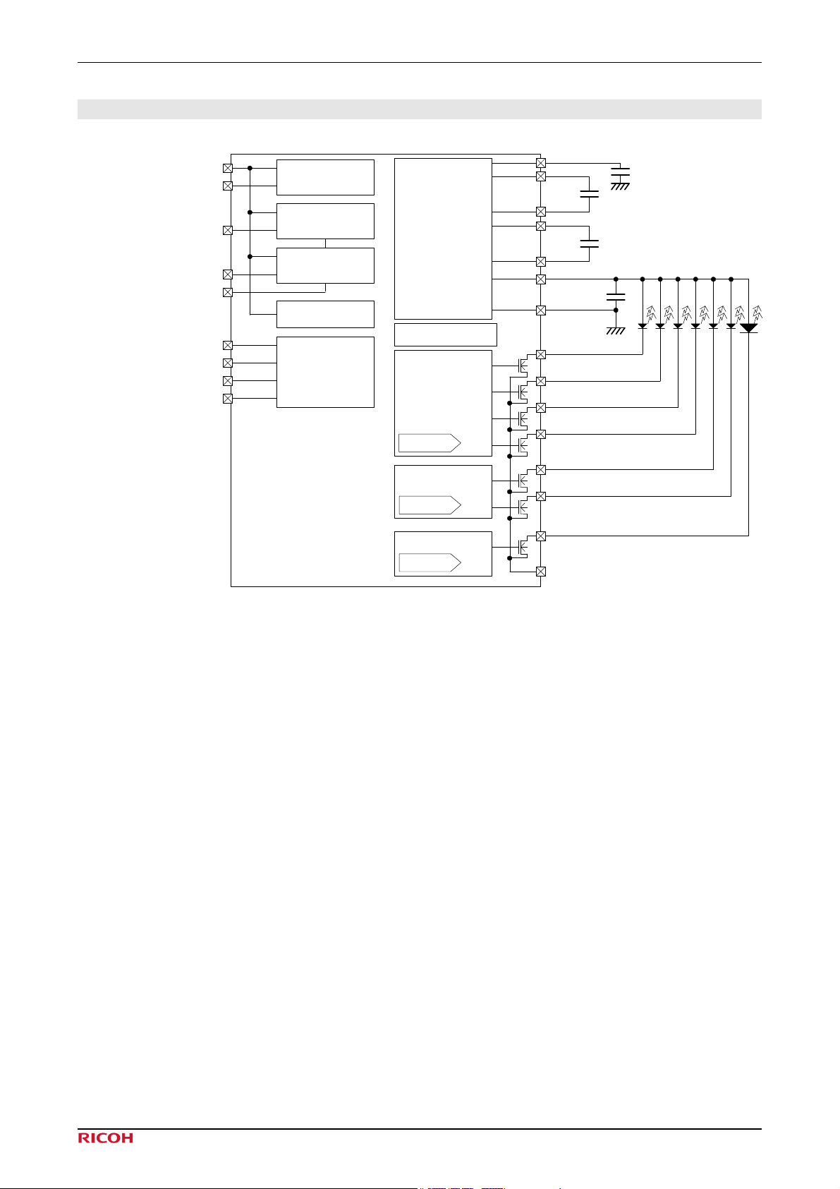
4. Block Diagram.......................................................................................................................................... 5
5. Pin Description ......................................................................................................................................... 6
6. Functional Blocks ..................................................................................................................................... 7
6.1 Regulators.............................................................................................................................................. 7
6.1.1 LDO1 Electrical Characteristics ................................................................................................................ 7
6.1.2 LDO2 Electrical Characteristics ................................................................................................................ 8
6.2 Thermal Shutdown Circuit....................................................................................................................... 9
6.2.1 Thermal Shutdown Block Diagram ........................................................................................................... 9
6.2.2 Thermal Shutdown Explanation of Operation...........................................................................................9
6.2.3 Thermal Shutdown Electrical Characteristics............................................................................................ 9
6.3 Charge Pump........................................................................................................................................ 10
6.3.1 Block Diagram......................................................................................................................................... 10
6.3.2 Operation ................................................................................................................................................. 11
6.3.3 Protection Circuit..................................................................................................................................... 12
6.3.4 Unused DIN_ Pin..................................................................................................................................... 12
6.3.5 Soft-start .................................................................................................................................................. 12
6.3.6 Charge Pump Electrical Characteristics................................................................................................... 13
6.3.7 STBB Logic Input ................................................................................................................................... 14
6.4 UVLO (Under Voltage Lock Out).......................................................................................................... 14
6.5 CPU Interface....................................................................................................................................... 15
6.5.1 Start and Stop Condition.......................................................................................................................... 15
6.5.2 Data Transmission and its Acknowledge................................................................................................. 16
6.5.3 I2C -Bus Slave Address........................................................................................................................... 16
6.5.4 Data Transmission Write Format............................................................................................................. 17
6.5.5 Internal Register Write-in Timing ........................................................................................................... 17
6.5.6 Connection of I2C-Bus............................................................................................................................ 18
6.5.7 AC Characteristics of I2C-Bus ................................................................................................................ 19
7. Register .................................................................................................................................................. 20
7.1 Register Map........................................................................................................................................ 20
7.2 Main / Sub / Flash / Strobe Luminance ................................................................................................... 21
Page 1 ©2009 Rev. 1.5
Page 3
RN5T652 Rev.1.5
7.3 LDO1 / LDO2 Output Voltage ............................................................................................................... 22
7.4 Others Function.................................................................................................................................... 22
8. Electrical Characteristics........................................................................................................................ 23
8.1 Absolute Maximum Ratings .................................................................................................................. 23
8.2 Recommendation of Operation Conditions.............................................................................................. 23
8.3 General Characteristics.......................................................................................................................... 23
8.4 DC Characteristics ................................................................................................................................24
9. Additional Application Circuit................................................................................................................ 25
10. Package Information .............................................................................................................................. 27
©2009 Rev. 1.5
Page 2
Page 4
RN5T652 Rev. 1.5
1. Outline
RN5T652 contains constant frequency charge pump to optimize for white LED application and two low-noise LDOs.
Output enable/disable, LEDs current setting and LDO output voltage setting are individually controllable through I2C.
2. Feature
z Power Supply Function
9 LDO × 2 (ON/OFF programmable)
9 Over current Protection (All Regulators) and thermal shutdown
z White LED Charge Pump
9 Current capability: All currents capability 450mA
9 Flash at 300mA max.
9 Four Main LEDs at 25mA max.
9 Two Sub LEDs 25mA max.
z I2C-Bus (Max: 400kHz)
9 Address = 64h
9 ON/OFF control
9 Individual LEDs current value setting
9 Individual LDOs voltage value setting
z Others
9 Soft-start circuit
9 Short-circuit protection, open-circuit and thermal protection
z Package
9 28pin thin QFN package (Body size: 4 x 4 x 0.8mm)
z Process
9 CMOS process
©2009 Rev. 1.5 Page 3
Page 5
RN5T652 Rev. 1.5
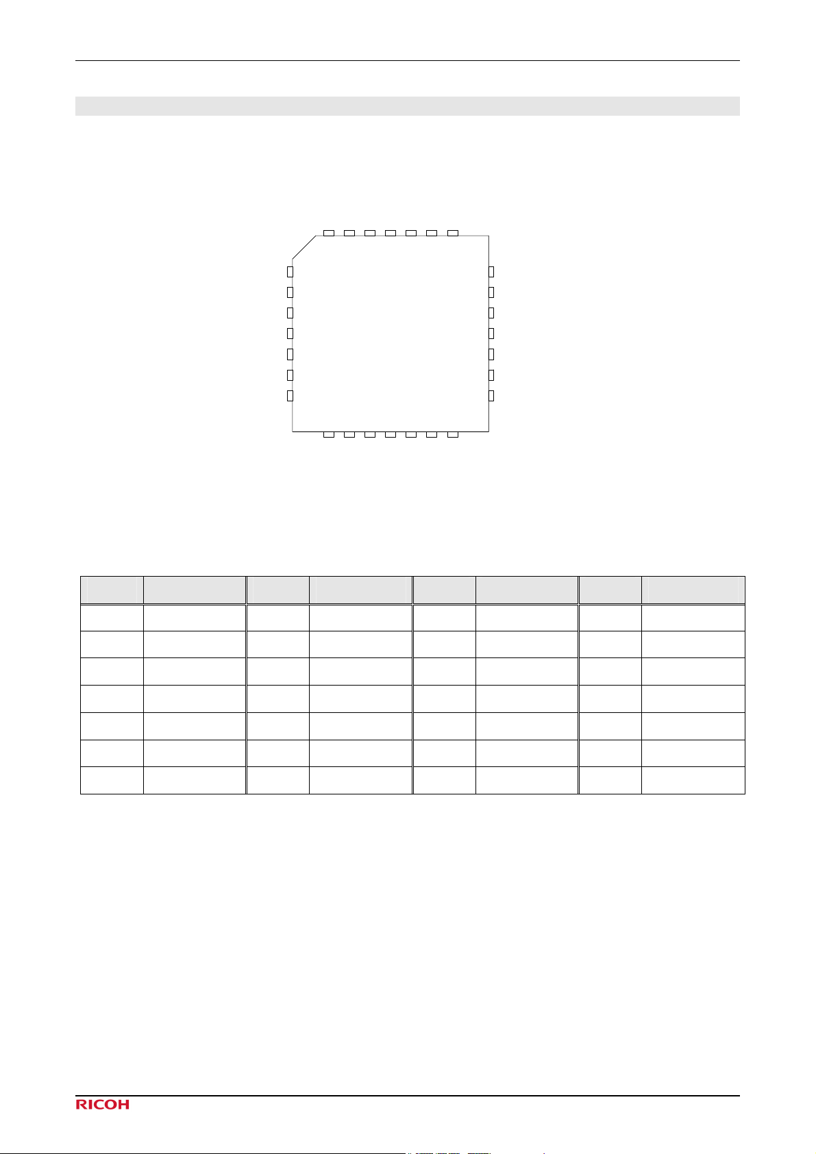
3. Pin Configuration
(TOP VIEW)
DIN3
DIN2
DIN1
VOUT
C1P
C2P
C2M
GND1
DIN5
DIN4
28
27
26
DIN6
25
1
2
3
4
RN5T652
5
6
7
10
C1M
VIN1
11
VEN
9
8
PGND1
DIN7
24
12
STBB
GND2
23
13
SCL
VREF
22
14
SDA
LDOUT1
21
VIN3
20
LDOUT2
19
N.C.
18
N.C.
17
N.C.
16
N.C.
15
QFN0404-28 pin
Pin No. Name Pin No. Name Pin No. Name Pin No. Name
1 DIN3 8 PGND1 15 N.C. 22 VREF
2 DIN2 9 C1M 16 N.C. 23 GND2
3 DIN1 10 VIN1 17 N.C. 24 DIN7
4 VOUT 11 VEN 18 N.C. 25 DIN6
5 C1P 12 STBB 19 LDOUT2 26 DIN5
6 C2P 13 SCL 20 VIN3 27 GND1
7 C2M 14 SDA 21 LDOUT1 28 DIN4
Fig 3-1 Pin Configuration
©2009 Rev. 1.5 Page 4
Page 6
RN5T652 Rev. 1.5
4. Block Diagram
VIN3
VREF
LDOUT1
LDOUT2
GND2
VEN
SCL
SDA
STBB
VREF
LDO1
LDO2
UVLO
Digital
Charge Pump
@450mA
Thermal
Shutdown
CC Driver
(Main)
5bit DAC
CC Driver (Sub)
5bit DAC
VIN1
C2P
1uF
C2M
C1P
1uF
C1M
VOUT
2.2uF
PGND1
DIN1
@25mA
DIN2
@25mA
DIN3
@25mA
DIN4
@25mA
DIN5
@25mA
DIN6
@25mA
4.7uF
GND
GND
CC Driver (Flash)
5bit DAC
Fig 4-1 Block Diagram
DIN7
@300mA
GND1
©2009 Rev. 1.5 Page 5
Page 7
RN5T652 Rev. 1.5
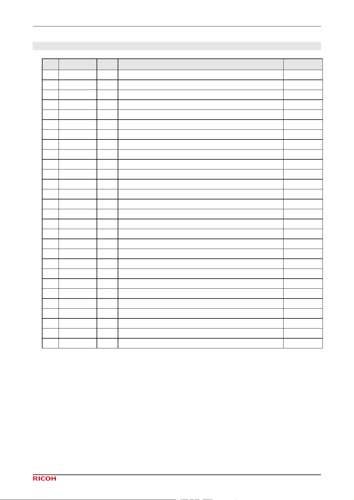
5. Pin Description
No. Name I/O
1 DIN3 O LED driver current control output 3
2 DIN2 O LED driver current control output 2
3 DIN1 O LED driver current control output 1
4 VOUT O LED driver voltage output
5 C1P - Charge pump boost capacitor connection
6 C2P - Charge pump boost capacitor connection
7 C2M - Charge pump boost capacitor connection
8 PGND1 - Ground (charge pump)
9 C1M - Charge pump boost capacitor connection
10 VIN1 - Power supply (charge pump)
11 VEN - Voltage supply (I2C), enable input
12 STBB I Strobe enable input
13 SCL I I2C interface clock input
14 SDA I/O I2C interface data input
15 N.C. - Non-connect
16 N.C. - Non-connect
17 N.C. - Non-connect
18 N.C. - Non-connect
19 LDOUT2 O LDO2 output
20 VIN3 - Power supply
21 LDOUT1 O LDO1 output
22 VREF O Bypass capacitor connecting pin
23 GND2 - Ground
24 DIN7 O LED driver current control output 7
25 DIN6 O LED driver current control output 6
26 DIN5 O LED driver current control output 5
27 GND1 - Ground
28 DIN4 O LED driver current control output 4
Function Notes
Table 5-1 Pin Description
©2009 Rev. 1.5 Page 6
Page 8
RN5T652 Rev. 1.5
6. Functional Blocks
6.1 Regulators
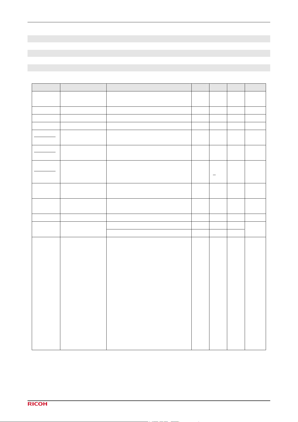
6.1.1 LDO1 Electrical Characteristics
Operating Conditions (Unless otherwise specified) V
BATT
= 3.6V, C
= 1μF, Ta = 25℃
REFO
Symbol Parameter Condition Min Typ Max Units
VOUT1 Output Voltage
50μA<IOUT1<300mA
VOUT1+0.5V≦V
BATT
(VIN)≦4.5V
-2% 1.50 +2% V
IOUT1 Output Current - 300 mA
ILIM1 Current Limit VOUT1=1.5V 500 mA
VDRP1 Drop-out Voltage IOUT1=200mA, Ta =85℃ 200 mV
ΔVOUT1
ΔVIN
ΔVOUT1
ΔIOUT1
ΔVOUT1
ΔT
a
Line Regulation
Load Regulation 50μA<IOUT1<300mA 25 mV
Output Voltage
Temperature
Coefficient
RR1 Ripple Rejection
EN1
Output Noise
(RMS)
VOUT1+0.5V≦V
BATT
IOUT1=150mA
-40℃≦T
≦85℃ +100 ppm/℃
a
f=10Hz-10kHz, C
IOUT1=30mA
BW=100Hz-100kHz, C
IOUT1=30mA
(VIN)≦4.5V
=2.2μF
out
=2.2μF
out
2.4 mV
60 dB
35 μVrms
BC1 Bypass Capacitor 0μA<IOUT1<300mA 2.2 μF
ISS1 Supply Current
Normal (IOUT1=Max) 50*1
OFF 1
μA
1.50
1.80
2.50
2.60
2.80
3.00
3.10
3.30
1.85 *
+2% V
POUT1
Programmable
Output Voltage
IOUT1=300mA -2%
2.40 *
2.55 *
2.70 *
2.85 *
2.90 *
3.20 *
Table 6-1 LDO1 Electrical Characteristics
Note*: Bypass capacitor: 2.2μF, in mounted state.
For optimized phase compensation, the bypass capacitor must be the ceramic type.
©2009 Rev. 1.5 Page 7
Page 9
RN5T652 Rev. 1.5
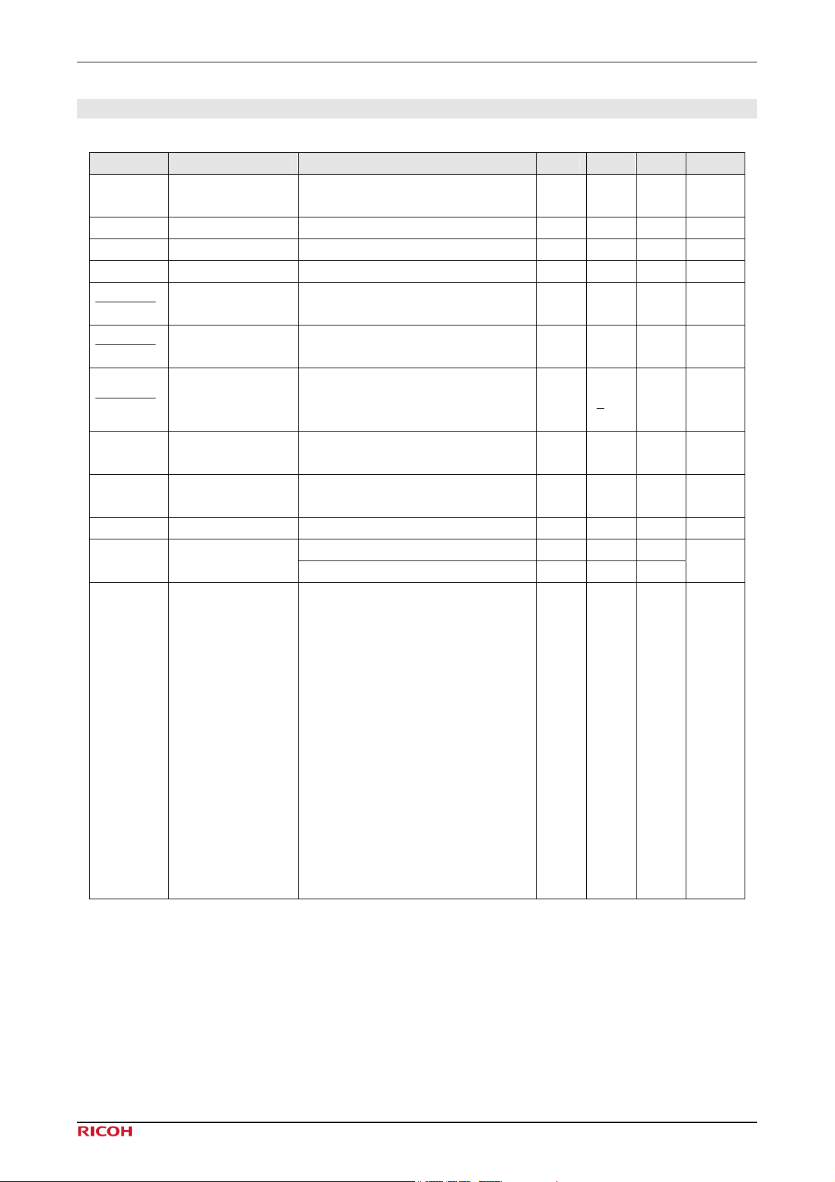
6.1.2 LDO2 Electrical Characteristics
Operating Conditions (Unless otherwise specified) VBATT = 3.6V, CREFO = 1μF, Ta = 25℃
Symbol Parameter Condition Min Typ Max Units
VOUT2 Output Voltage
50μA<IOUT2<300mA
VOUT2+0.5V≦V
BATT
(VIN)≦4.5V
-2% 1.50 +2% V
IOUT21 Output Current - 300 mA
ILIM2 Current Limit VOUT2=1.5V 500 mA
VDRP2 Drop-out Voltage IOUT2=200mA, Ta =85℃ 200 mV
ΔVOUT2
ΔVIN
ΔVOUT2
ΔIOUT2
ΔVOUT2
ΔT
a
Line Regulation
Load Regulation 50μA<IOUT2<300mA 25 mV
Output Voltage
Temperature
Coefficient
RR2 Ripple Rejection
EN2
Output Noise
(RMS)
VOUT2+0.5V≦V
BATT
IOUT2=150mA
-40℃≦T
≦85℃ +100 ppm/℃
a
f=10Hz-10kHz, C
IOUT2=30mA
BW=100Hz-100kHz, C
IOUT2=30mA
(VIN)≦4.5V
=2.2μF
out
=2.2μF
out
2.4 mV
60 dB
35 μVrms
BC2 Bypass Capacitor 0μA<IOUT2<300mA 2.2 μF
ISS2 Supply Current
Normal (IOUT2=Max) 50*1
μA
OFF 1
1.50
1.80
2.50
2.60
2.80
3.00
3.10
3.30
1.85 *
+2% V
POUT2
Programmable
Output Voltage
IOUT2=300mA -2%
2.40 *
2.55 *
2.70 *
2.85 *
2.90 *
3.20 *
Table 6-2 LDO2 Electrical Characteristics
Note*: Bypass capacitor: 2.2μF, in mounted state.
For optimized phase compensation, the bypass capacitor must be the ceramic type.
Note*1: Vref Block Supply Current typ 20μA
ex)LDO1+LDO2+Vref =120μA(typ)
LDO1+Vref=70μA(typ)
©2009 Rev. 1.5 Page 8
Page 10
RN5T652 Rev. 1.5
6.2 Thermal Shutdown Circuit
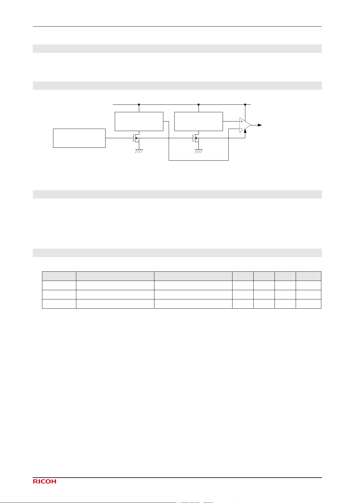
The thermal shutdown circuit is consisted of two temperature detection circuits and an op-amp.
6.2.1 Thermal Shutdown Block Diagram
VIN
Temperature
Detection Circuit
Control Circuit
GND
Temperature
Detection Circuit
GND
To Power-on
Control Circuit
Fig 6-1 Thermal Shutdown Circuit Diagram
6.2.2 Thermal Shutdown Explanation of Operation
The overheat state can be detected by comparing the output voltages from two temperature detection circuits, which
have different temperature characteristics. If the overheat state is detected, the internal POWERSW signal will fall
down to “L” and RN5T652 will turn off to protect itself from overheating.
6.2.3 Thermal Shutdown Electrical Characteristics
Operating Conditions (Unless otherwise specified) V
BATT
= 3.6V, C
= 1μF, Ta = 25℃
REFO
Symbol Parameter Condition Min Typ Max Units
T
Detected Temperature - 150 ℃
DET
T
Return Temperature - 100 ℃
RET
ISS Supply Current - 10 20 μA
Table 6-3 Thermal Shutdown Electrical Characteristics
©2009 Rev. 1.5 Page 9
Page 11
RN5T652 Rev. 1.5
6.3 Charge Pump
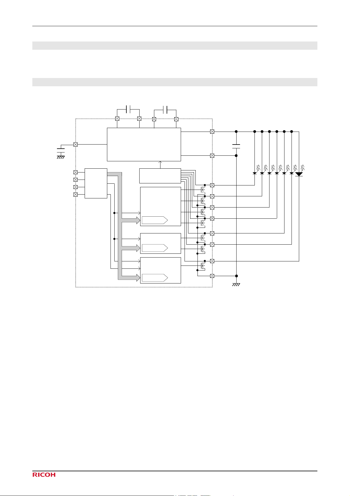
RN5T652 charge pump drives up to six white LEDs and one strobe with regulated constant current for uniform
intensity.
6.3.1 Block Diagram
4.7 µ F
VIN1
GND
VEN
SCL
SDA
STBB
Logic
C1M
1µF
C1P
Charge Pump
@450mA
ON/OFF
ON/OFF
ON/OFF
STBB
CC Driver (Sub)
CC Driver (Flash)
1µF
C2M
Adjust
Voltage
CC Driver
(Main)
5bit DAC
5bit DAC
5bit DAC
C2P
VOUT
2.2 µ F
PGND1
Feed Back
DIN1
@25mA
DIN2
@25mA
DIN3
@25mA
DIN4
@25mA
DIN5
@25mA
DIN6
@25mA
DIN7
@300mA
GND1
Fig 6-2 Charge Pump Circuit Diagram
GND
©2009 Rev. 1.5 Page 10
Page 12
RN5T652 Rev. 1.5
6.3.2 Operation
Initial and 1x mode
When any channel is turned ON, charge pump output (VOUT) voltage becomes VIN1 voltage. In this time, Soft-start
prevents the inrush current. As a result, RN5T652 starts at 1x mode.
In 1x mode, the following relation is the condition to stay in 1x mode.
VOUT - Vf > 0.25V (1)
Here, VOUT and Vf mean output of Charge pump and forward voltage of white LED, respectively. 0.25V means mode
transition threshold, in case of setting at 25mA of Main or Sub.
1x or 1.5x transition
When the battery voltage decreases and DIN_ pin voltage becomes lower than 0.25V for 100us, RN5T652 starts
charge pump in 1.5x mode.
In 1.5x mode, the following relation is the condition to stay in 1.5x mode.
VOUT - Vf > 0.25V (2)
In 1.5x mode, CP is switched to 1x mode about every 1 sec and judge the mode whether 1x or 1.5x for 100us.
1.5x or 2x transition
When the battery voltage decreases furthermore, and DINx_ pin voltage goes down below 0.25V for 100us, RN5T652
starts 2x mode from 1.5x mode. In 2x mode, CP is switched to 1.5x mode about every 1 sec and judge the mode
whether 2x or 1.5x for 100us.
1x/1.5x/2x mode transition
©2009 Rev. 1.5 Page 11
Page 13
RN5T652 Rev. 1.5
6.3.3 Protection Circuit
When any DIN_ pin is floating or grounded, VOUT voltage is limited below protection voltage by gating on/off charge
pump. In case any LED fails as an open circuit, VOUT voltage is also limited. Besides, when VOUT is smaller than
approximately 1.2V, charge pump also stops.
6.3.4 Unused DIN_ Pin
In case there is any unused DIN_ pin, connect DIN_ to GND to avoid over voltage protection status.
6.3.5 Soft-start
When LEDs are turned ON, to prevent the inrush current, RN5T652 has the soft-start function. (The internal resistance
gradually increases, just after LEDs enabled.)
©2009 Rev. 1.5 Page 12
Page 14
RN5T652 Rev. 1.5
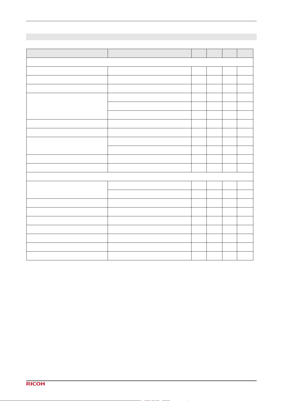
6.3.6 Charge Pump Electrical Characteristics
Unless otherwise specified VIN=3.6V, Ta=25℃, C1=C2=1uF, Cout=2.2uF
Parameter Conditions Min Typ Max Units
Charge Pump
Operating Voltage VIN1 and VIN3 voltage 2.7 4.5 V
VOUT voltage (Over voltage) Repeat On and Off in 1.5x or 2x 4.8 V
Maximum Output current VIN1=3.6V, VOUT=4.2V 450 mA
1x mode 1 Ohm
Output resistance: Ro
1.5x mode 3 Ohm
2x mode 6 Ohm
Switching Frequency - 1.25 MHz
Soft-start time - 0.18 msec
1x mode, No load, (DET, Reference ON) 0.8 mA
Supply current
1.5x mode or 2x mode 5 6 mA
Standby supply current VEN=0V, VIN1 and VIN3 current 1 uA
Current Limit VOUT shorted 50 mA
LED Driver
DIN1-6 25 mA
Maximum Sink current
DIN7 300 mA
LED current accuracy (Main, Sub) Code=1F, DIN_=0.25V -5 5 %
LED current accuracy (Flash) Code=1F, DIN7=0.4V -5 5 %
LED current matching Main or Sub, respectively*1 -5 5 %
1x to 1.5x, 1.5x to 2x transition threshold At lowest DINx pin, DIN1-6 250 mV
1x to 1.5x, 1.5x to 2x transition threshold At lowest DINx pin, DIN7 400 mV
1x to 1.5x, 1.5x to 2x transition time Chattering noise reduction 100 us
DIN1-7 leakage in shutdown - 0.01 uA
Table 6-4 Charge Pump Electrical Characteristics
Note*1: Matching is defined (Iave_ - Iled_) / Iave_. Iave_ means the average current of Main or Sub, respectively.
Matching is defined without Vf voltage difference between channels.
For Main, Iave_main = (Iled1 + Iled2 + Iled3 + Iled4) / 4
For Sub, Iave_sub = (Iled5 + Iled6) / 2
©2009 Rev. 1.5 Page 13
Page 15
RN5T652 Rev. 1.5
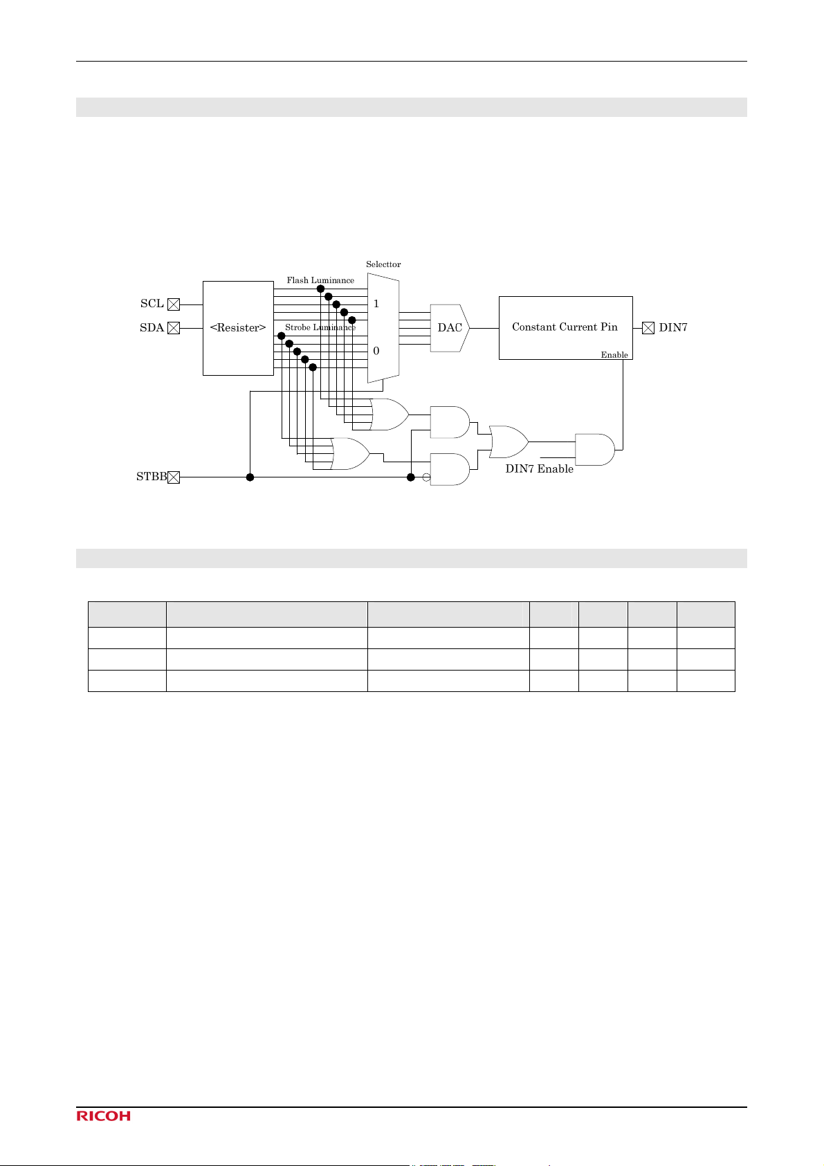
6.3.7 STBB Logic Input
STBB input is used to control the flash LEDs without accessing I2C. When STBB is driven to "L", the flash LEDs are
driven by the current set in the strobe luminance register.
Driving STBB low overrides the flash LEDs set by I2C. With STBB high, the flash LEDs becomes controllable by I2C
interface.
Fig 6-3 STBB Input Diagram
6.4 UVLO (Under Voltage Lock Out)
Operating Conditions (Unless otherwise specified) C
Symbol Parameter Condition Min Typ Max Units
V
Under voltage lock out threshold VCCVIN rising 2.25 V
Release
V
Under voltage lock out threshold VCCVIN falling 2.05 2.20 2.35 V
Detect
V
UVLO Hysteresis - 50 mV
HYS
Table 6-5 UVLO Electrical Characteristics
= 1μF, Ta = 25℃
REFO
©2009 Rev. 1.5 Page 14
Page 16
RN5T652 Rev. 1.5
6.5 CPU Interface
RN5T652 uses I2C-Bus system for CPU connection through 2-wires. Connection and transfer system of I2C-Bus are
described in the following sections.
6.5.1 Start and Stop Condition
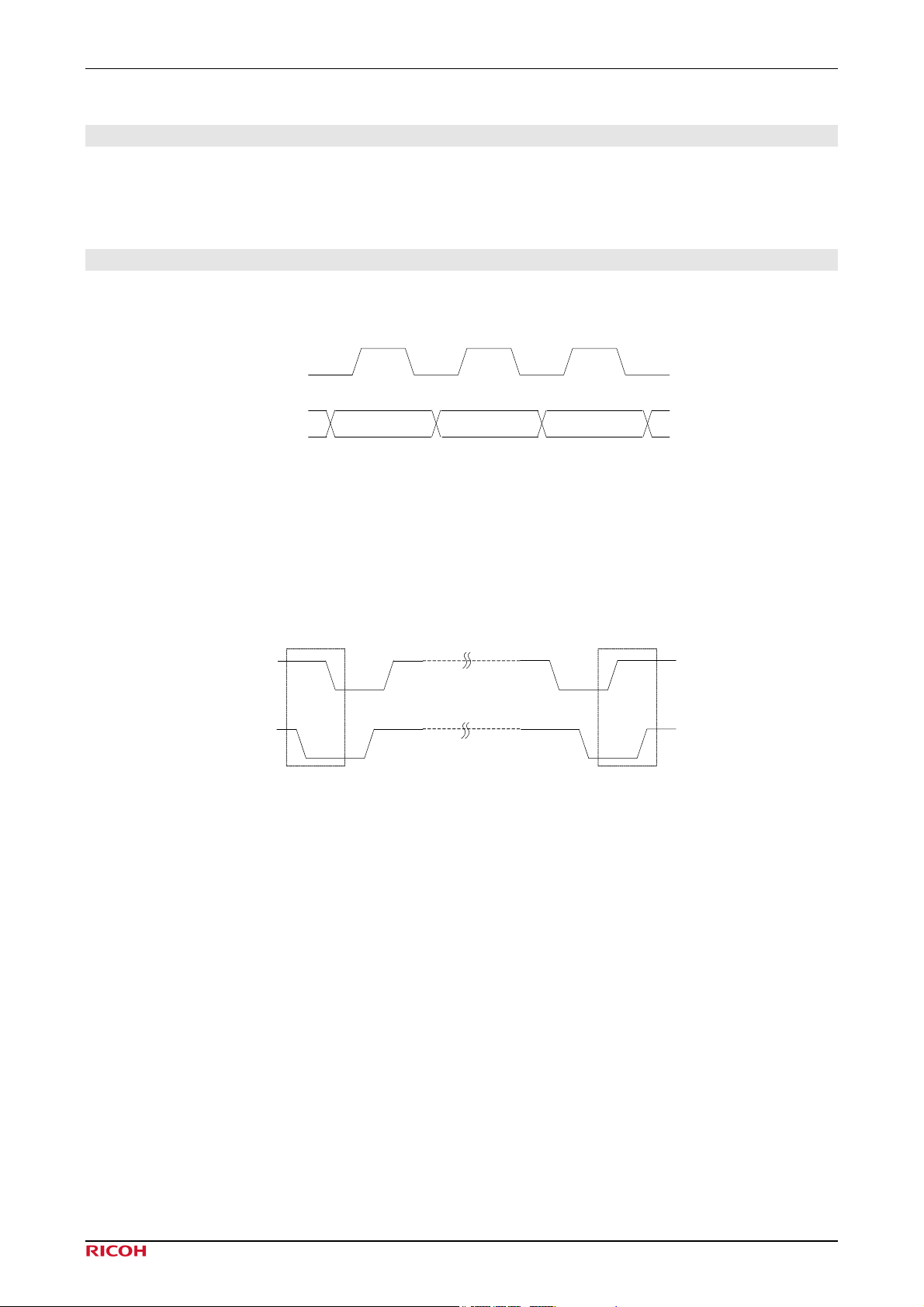
Within the procedure of I2C-Bus, unique situations which are defined as Start and Stop conditions arise.
SCL
SDA
Fig 6-4 I2C-Bus Data Transmission
An “H” to “L” transition on SDA line while SCL is “H” indicates a Start condition. An “L” to “H” transition on SDA
line while SCL is “H” defines a Stop condition. Start and Stop conditions are always generated by master (Refer to the
figure below). The bus is considered to be busy after the Start condition. The bus is considered to be free again a certain
time after the stop condition.
Start Condition Stop Condition
SCL
SDA
Fig 6-5 I2C-Bus Start and Stop Condition
©2009 Rev. 1.5 Page 15
Page 17
RN5T652 Rev. 1.5
6.5.2 Data Transmission and its Acknowledge
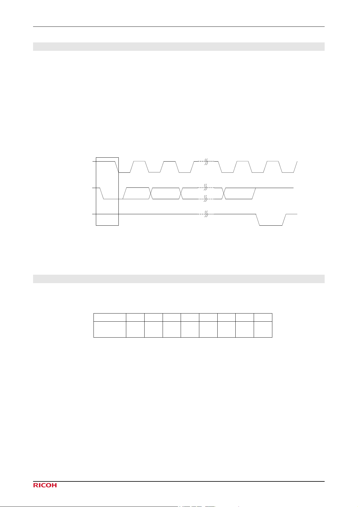
After start condition, data is transmitted by 1byte (8bits). The number of bytes that can be transmitted per transmission
is not limited. Receiver must send an acknowledge signal to the transmitter every time 8bit data is transmitted.
Data transmission must be accompanied by acknowledge signal. The acknowledge-related clock pulse is generated by
the master. The transmitter releases SDA line during the acknowledge clock pulse.
The receiver must pull down SDA line during the acknowledge clock pulse so that it remains stable “L” during “H”
period of this clock pulse.
If a master–receiver is involved in a transfer, it must signal the end of the data to the slave-transmitter by not generating
an acknowledge signal on the last byte that was clocked out of the slave. The slave-transmitter must release the data line
to allow the master to generate a Stop condition.
SCL from
Master
SDA from
Transmitter
SDA from
Receiver
Start Condition
12 89
Acknowledge Signal
Fig 6-6 I2C-Bus Data Transmission and its Acknowledge
6.5.3 I2C -Bus Slave Address
After the start condition, a slave address is sent. This address is 8 bits long followed by. The slave address of RN5T652
are specified at “0110 0100b”
A7 A6 A5 A4 A3 A2 A1 A0
Setting
value
0 1 1 0 0 1 0 0
A7~A0: Slave Address
Fig 6-7 Slave Address of RN5T652
©2009 Rev. 1.5 Page 16
Page 18
RN5T652 Rev. 1.5
6.5.4 Data Transmission Write Format
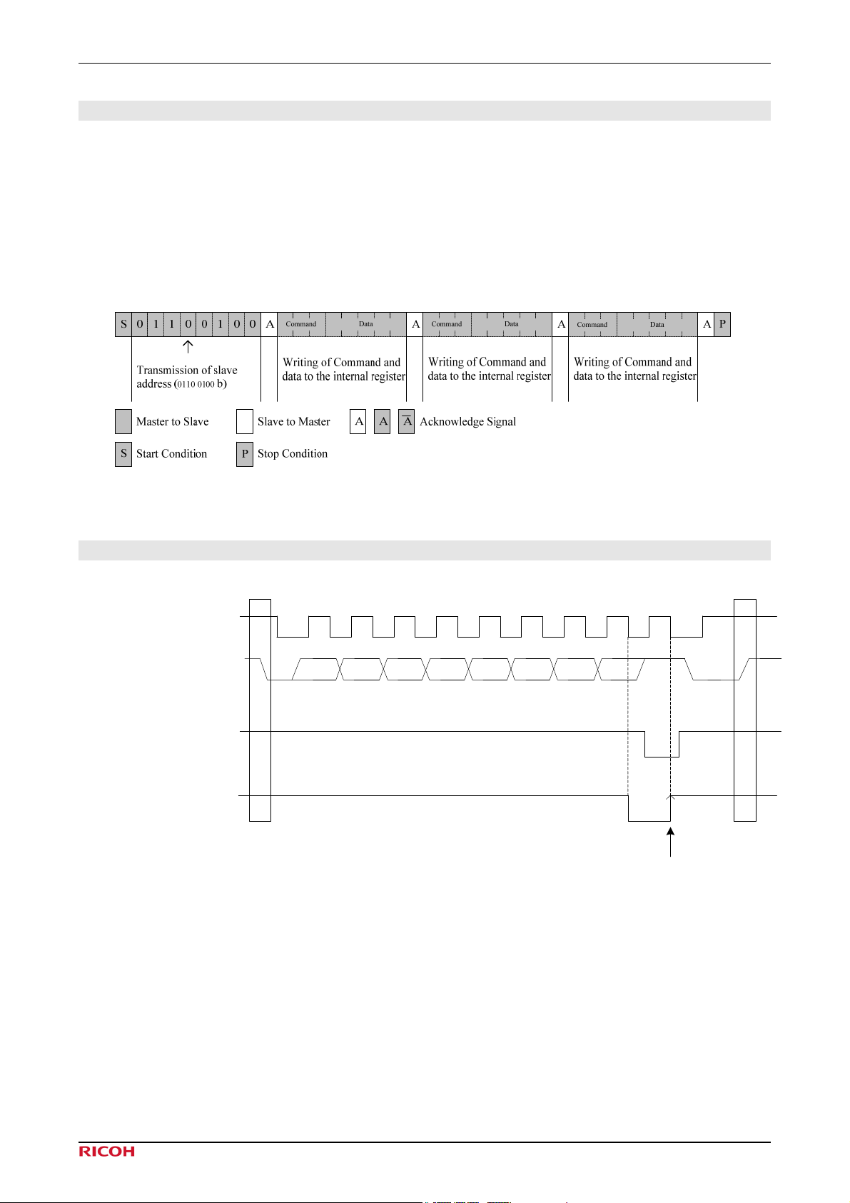
The transmission format for the slave address allocated to each IC is defined by I2C-Bus standard. However
transmission method of address information of each IC is not defined. RN5T652 transmits data to the internal address
pointer at 1byte continue to the slave address and write command. For the data transmission, please transmit MSB first
from Master and following data in sequence. Also, Master should receive MSB first when it receives data from the
slave.
6.5.5 Internal Register Write-in Timing
SCL from Master
SDA from Master
SDA from Slave
An Internal Register
Write-in Signal (WRB)
Start Condition
Fig 6-8 Data Transmission Write Format
198765423
Acknowledge
Stop Condition
Writing to an internal register
Fig 6-9 Internal Register Write-in Timing
©2009 Rev. 1.5 Page 17
Page 19
RN5T652 Rev. 1.5
6.5.6 Connection of I2C-Bus
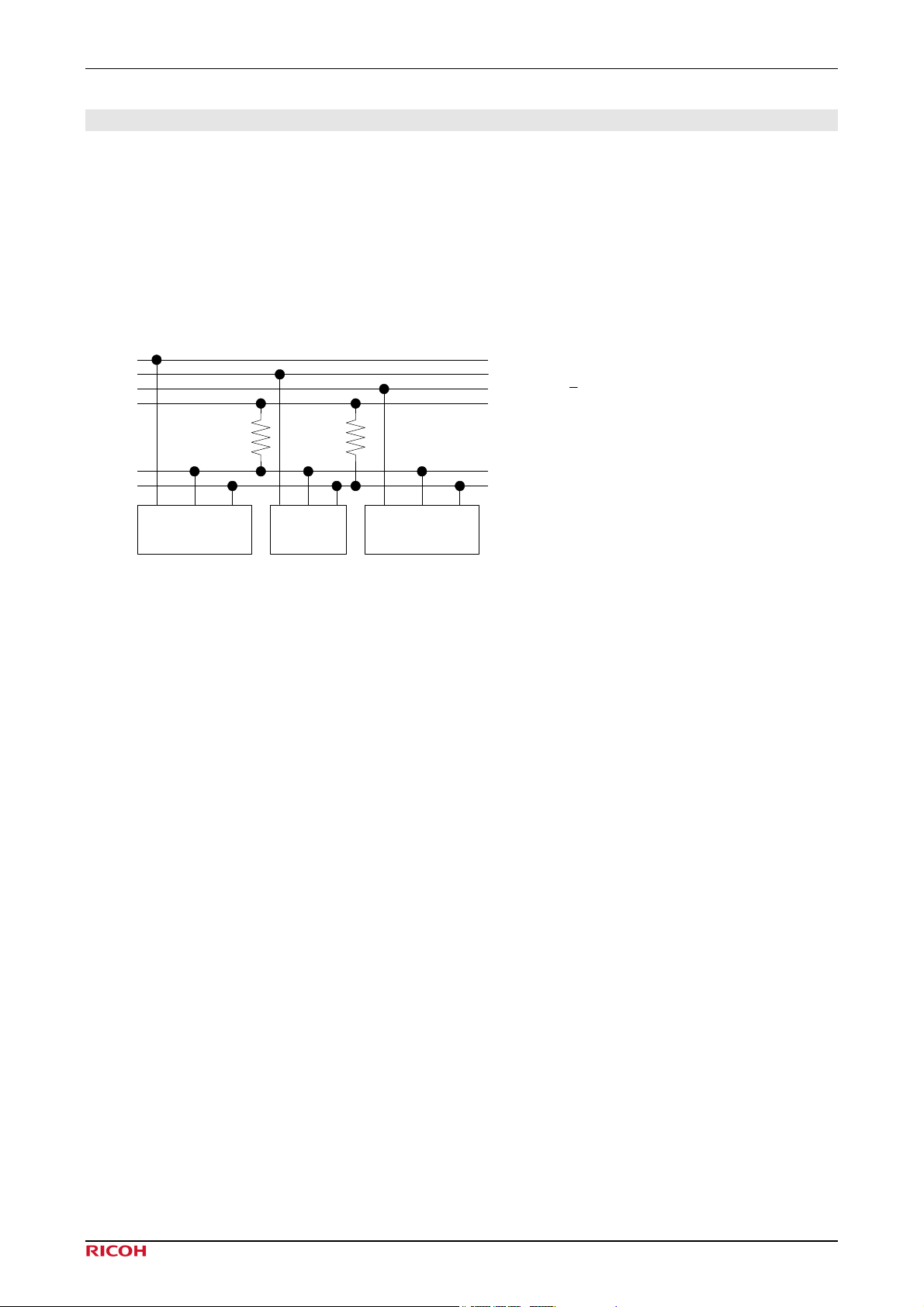
2 wires of SCL and SDA are connected to I2C-Bus and used for transmitting clock pulses and data individually. All ICs
connected to these two lines are designed not to be clamped even though voltage, which exceeds its power supply
voltage, is supplied through the input and output pins. Open drain pins is for output. This construction allows
communication of signals between Ics, which have different supply voltages, by adding a pull-up resistor to each signal
line as shown in the figure below. Each IC is designed not to give any effect on SCL and SDA signal lines even though
their power is turned off individually.
VDD1
DD2
V
V
DD3
DD4
V
SCL
SDA
R
P RP
Microcontroller RN5T652
*1) For data interface, the following conditions must be met :
V
DD4 > VDD1
V
DD4 > VDD2
V
DD4 > VDD3
*2) When the master is one, the microcontroller is ready for
driving SCL to "H" and R
Other Periphral
IC
Fig 6-10 Connection of I2C-Bus
P of SCL may not be required.
©2009 Rev. 1.5 Page 18
Page 20
RN5T652 Rev. 1.5
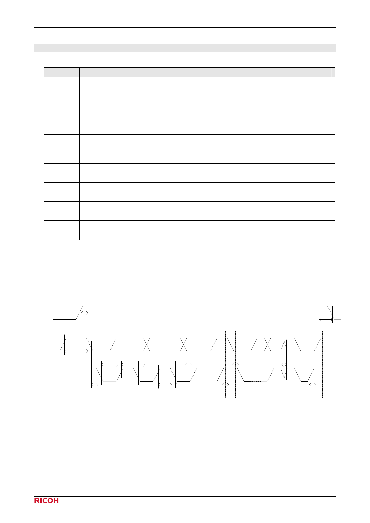
6.5.7 AC Characteristics of I2C-Bus
Operating Conditions (Unless otherwise specified) V
BATT
= 3.6V, C
= 1μF, Ta = 25℃
REFO
Symbol Parameter Condition Min Typ Max Units
f
SCL Clock Frequency - 400 kHz
SCL
t
BUF
t
SCL Clock “L” Time - 1.3 μs
LOW
t
SCL Clock “H” Time - 0.6 μs
HIGH
t
Start Condition Setup Time - 0.6 μs
SU;STA
t
Start Condition Hold Time - 0.6 μs
HD;STA
t
Stop Condition Setup Time - 0.6 μs
SU;STO
t
HD;DAT
t
Data Setup Time -
SU;DAT
Bus Free Time Between
a Precedent and Start
Data Hold Time - 0 μs
- 1.3 μs
100
*1
ns
tR Rising Time of SCL and SDA (Input) - 300 ns
tF Falling Time of SCL and SDA (Input) - 300 ns
tSP
t
VENSET
t
VENHOLD
Spike Width that can be
Removed with Input Filter
VEN to Start Condition Setup Time - 100 μs
VEN to Stop Condition Hold Time - 100 μs
- 50 ns
Table 6-6 AC Characteristics
Note*: All the above-mentioned values are corresponding to V
minimum and V
IH
maximum level.
IL
Note*1: Standard mode is allowed in I2C-Bus standard. For Standard mode, it needs to satisfy the condition;
tSU;DAT>=250ns.
t
BUF
t
HD;STA
t
VENSET
t
LOW
t
VENHOLD
t
R
t
HD;DAT
t
HIGHtF
t
SU;DAT
t
SU;STA
t
HD;STA
t
SP
t
SU;STO
VEN
SDA
SCL
PS Sr P
Fig 6-11 AC Characteristics of I2C-Bus
©2009 Rev. 1.5 Page 19
Page 21
RN5T652 Rev. 1.5
7. Register
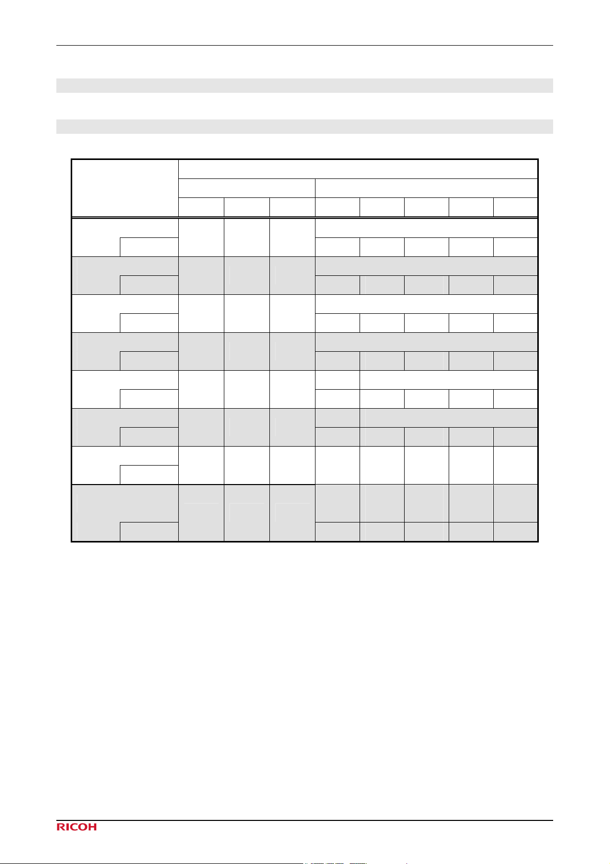
7.1 Register Map
SDA Control Byte
Function
COMMAND DATA
C2 C1 C0 D4 D3 D2 D1 D0
Main Luminance 31-steps 25mA / LED max. 000 00000 = off
Initial value
Flash Luminance 31-steps 300mA max, I2C enabled, 010 00000 = off
Initial value
Strobe Luminance 31-steps 300mA max, STBB enable, 011 00000 = off
Initial value
LDO1 Output Voltage x 16 steps
Initial value
LDO2 Output Voltage x 16 steps
Initial value
Initial value
Initial value
Sub Luminance 31-steps 25mA / LED max. 001 00000 = off
Test
0 0 0
0 0 0 0 0
0 0 1
0 0 0 0 0
0 1 0
0 0 0 0 0
0 1 1
0 0 0 0 0
1 0 0
0 0 0 0 0
1 0 1
0 0 0 0 0
1 1 0 0 0 0 0 0
Other Functions
1 1 1
Initial value
Table 7-1 Register Map
Note*: C2 is MSB, and D0 is LSB
Do not write “1”in Test Register [D4:D0].
Main
Enable
0 0 0 0 0
Sub
Enable
DIN7
Enable
LDO1
Enable
LDO2
Enable
©2009 Rev. 1.5 Page 20
Page 22
RN5T652 Rev. 1.5
7.2 Main / Sub / Flash / Strobe Luminance
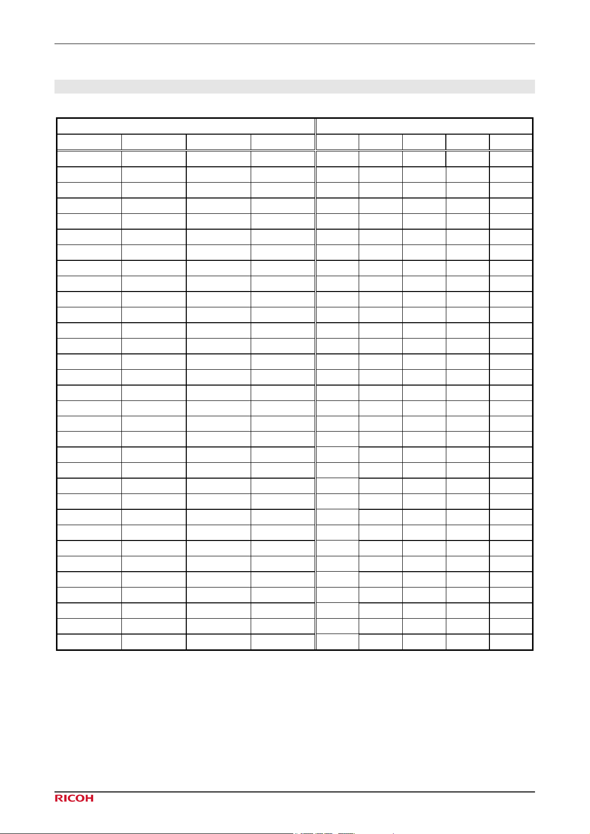
Each sink current of DIN1-4, 5, 6, and 7 can be set by the code of D4-D0.
LED Current (mA) Data
Main Sub Flash Strobe D4 D3 D2 D1 D0
off off off off 0 0 0 0 0
0.8 0.8 9.7 9.7 0 0 0 0 1
1.6 1.6 19.4 19.4 0 0 0 1 0
2.4 2.4 29.0 29.0 0 0 0 1 1
3.2 3.2 38.7 38.7 0 0 1 0 0
4.0 4.0 48.4 48.4 0 0 1 0 1
4.8 4.8 58.1 58.1 0 0 1 1 0
5.6 5.6 67.7 67.7 0 0 1 1 1
6.5 6.5 77.4 77.4 0 1 0 0 0
7.3 7.3 87.1 87.1 0 1 0 0 1
8.1 8.1 96.8 96.8 0 1 0 1 0
8.9 8.9 106 106 0 1 0 1 1
9.7 9.7 116 116 0 1 1 0 0
10.5 10.5 126 126 0 1 1 0 1
11.3 11.3 135 135 0 1 1 1 0
12.1 12.1 145 145 0 1 1 1 1
12.9 12.9 155 155 1 0 0 0 0
13.7 13.7 165 165 1 0 0 0 1
14.5 14.5 174 174 1 0 0 1 0
15.3 15.3 184 184 1 0 0 1 1
16.1 16.1 194 194 1 0 1 0 0
16.9 16.9 203 203 1 0 1 0 1
17.7 17.7 213 213 1 0 1 1 0
18.5 18.5 223 223 1 0 1 1 1
19.4 19.4 232 232 1 1 0 0 0
20.2 20.2 242 242 1 1 0 0 1
21.0 21.0 252 252 1 1 0 1 0
21.8 21.8 261 261 1 1 0 1 1
22.6 22.6 271 271 1 1 1 0 0
23.4 23.4 281 281 1 1 1 0 1
24.2 24.2 290 290 1 1 1 1 0
25.0 25.0 300 300 1 1 1 1 1
Note*: Defaults shown in Bold.
©2009 Rev. 1.5 Page 21
Page 23
RN5T652 Rev. 1.5
7.3 LDO1 / LDO2 Output Voltage
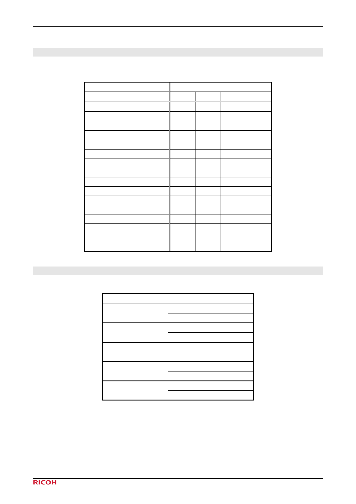
Each output voltage of LDO1 and LDO2 can be set by the code of D3-D0. And enable/disable of the output can be
individually set by D4 bit.
LDO Voltage (V) Data
LDO1 LDO2 D3 D2 D1 D0
1.50 1.50 0 0 0 0
1.80 1.80 0 0 0 1
2.50 2.50 0 0 1 0
2.60 2.60 0 0 1 1
2.80 2.80 0 1 0 0
3.00 3.00 0 1 0 1
3.10 3.10 0 1 1 0
3.30 3.30 0 1 1 1
1.85 1.85 1 0 0 0
2.40 2.40 1 0 0 1
2.55 2.55 1 0 1 0
2.70 2.70 1 0 1 1
2.85 2.85 1 1 0 0
2.90 2.90 1 1 0 1
3.20 3.20 1 1 1 0
1.50 1.50 1 1 1 1
7.4 Others Function
Bit DATA Function
D4 Main Enable
D3 Sub Enable
D2 DIN7 Enable
D1 LDO1 Enable
D0 LDO2 Enable
Note*: The relations between each bit of the other function register and each register are AND conditions.
1 Enable
0 Disable
1 Enable
0 Disable
1 Enable
0 Disable
1 Enable
0 Disable
1 Enable
0 Disable
©2009 Rev. 1.5 Page 22
Page 24
RN5T652 Rev. 1.5
8. Electrical Characteristics
8.1 Absolute Maximum Ratings
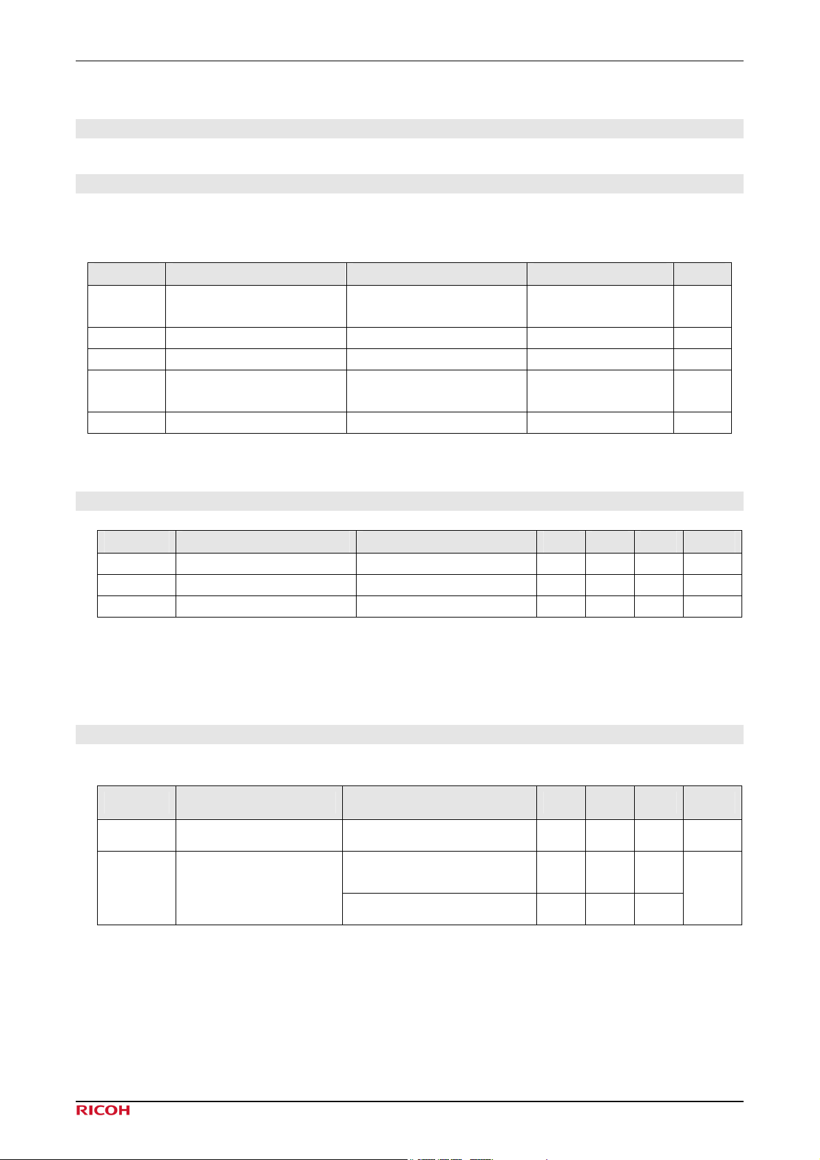
The operation exceeding “Absolute Maximum Ratings” below may cause permanent damage to the device.
The operation of the device within the stated ratings below is not guaranteed.
Symbol Parameter Condition Rated value Units
VIN1
VIN3
VEN Power Supply Voltage - -0.3~4.5 V
VIN Input Voltage Range All Input Pins -0.3~VEN+0.3 V
PD
T
Storage Temperature - -55~+125 ℃
stg
Power Supply Voltage Battery Voltage Input Pins -0.3~6.0 V
Package
Allowable Dissipation
Mounted on Board,
T
=70℃
a
1826 mW
8.2 Recommendation of Operation Conditions
Symbol Parameter Condition Min Typ Max Units
VIN Power Supply Voltage1 Battery Voltage Input Pins 2.7 3.6 4.5 V*
VEN Power Supply Voltage - 1.8 2.85 3.6 V
Ta Temperature of Operation - -40 +85 ℃
Note*: For safety operation of RN5T652, VEN pin should be connected to constant voltage source
in the recommended input voltage.
8.3 General Characteristics
Symbol Parameter Condition Min Typ Max Units
ISSVEN VEN Supply Current SCL=SDA=STBB=VEN 1 μA
ISHUT
Shutdown Supply Current
(All output off)
VEN=3.0V, I2C ready,
TA=25℃
VEN=0V, I2C off, TA=25℃ 1
3
μA
©2009 Rev. 1.5 Page 23
Page 25
RN5T652 Rev. 1.5
8.4 DC Characteristics
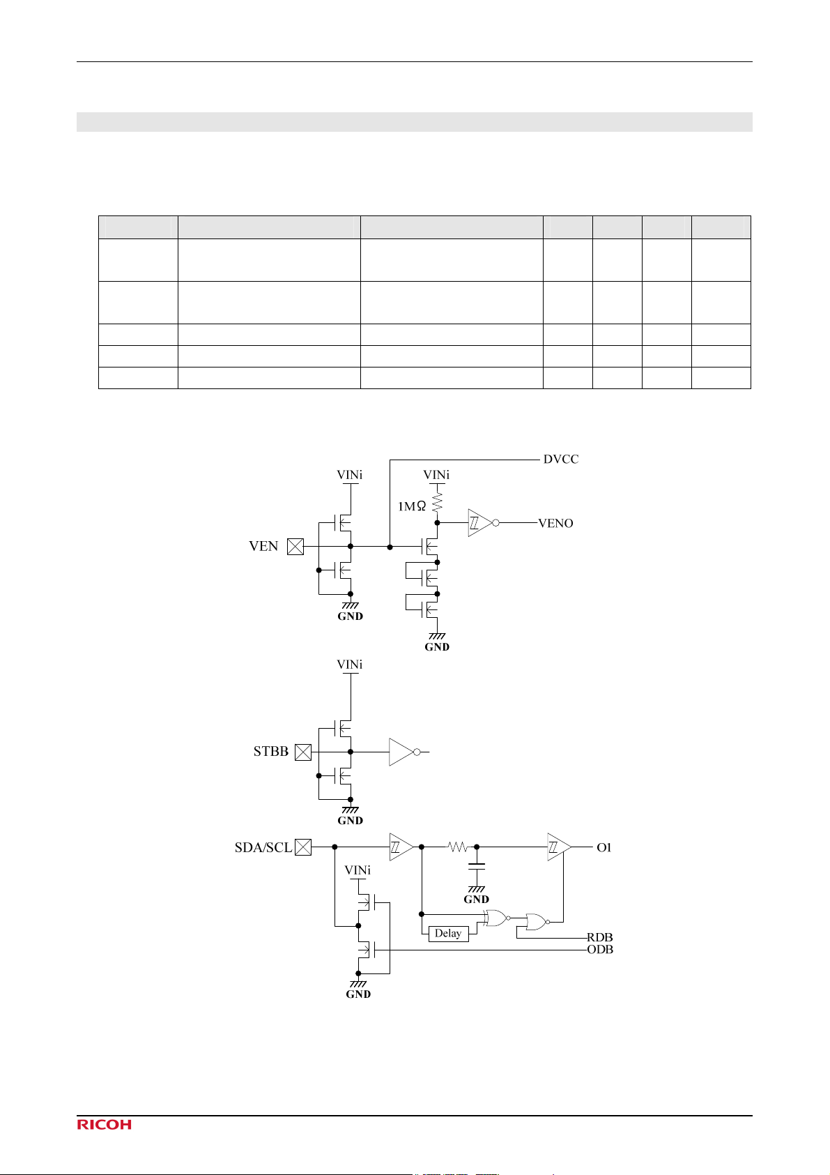
Digital Part Input
(Input pin) SCL, SDA, STBB
Operating Conditions (Unless otherwise specified) V
BATT
= 3.6V, C
= 1μF, Ta = 25℃
REFO
Symbol Parameter Condition Min Typ Max Units
VIH “H” Input Voltage -
VIL “L” Input Voltage -
VEN
x 0.7
V
VEN
x0.3
V
VOL “L” Output Voltage IOL=-3mA 0.3 V
IIL Input Leakage Current V=0~VEN -3 3 μA
IOZ Off Leakage Current V=0~VEN -3 3 μA
Terminal equivalent circuit
Fig 8-1 Terminal Equivalent Circuit
©2009 Rev. 1.5 Page 24
Page 26
RN5T652 Rev. 1.5
9. Additional Application Circuit
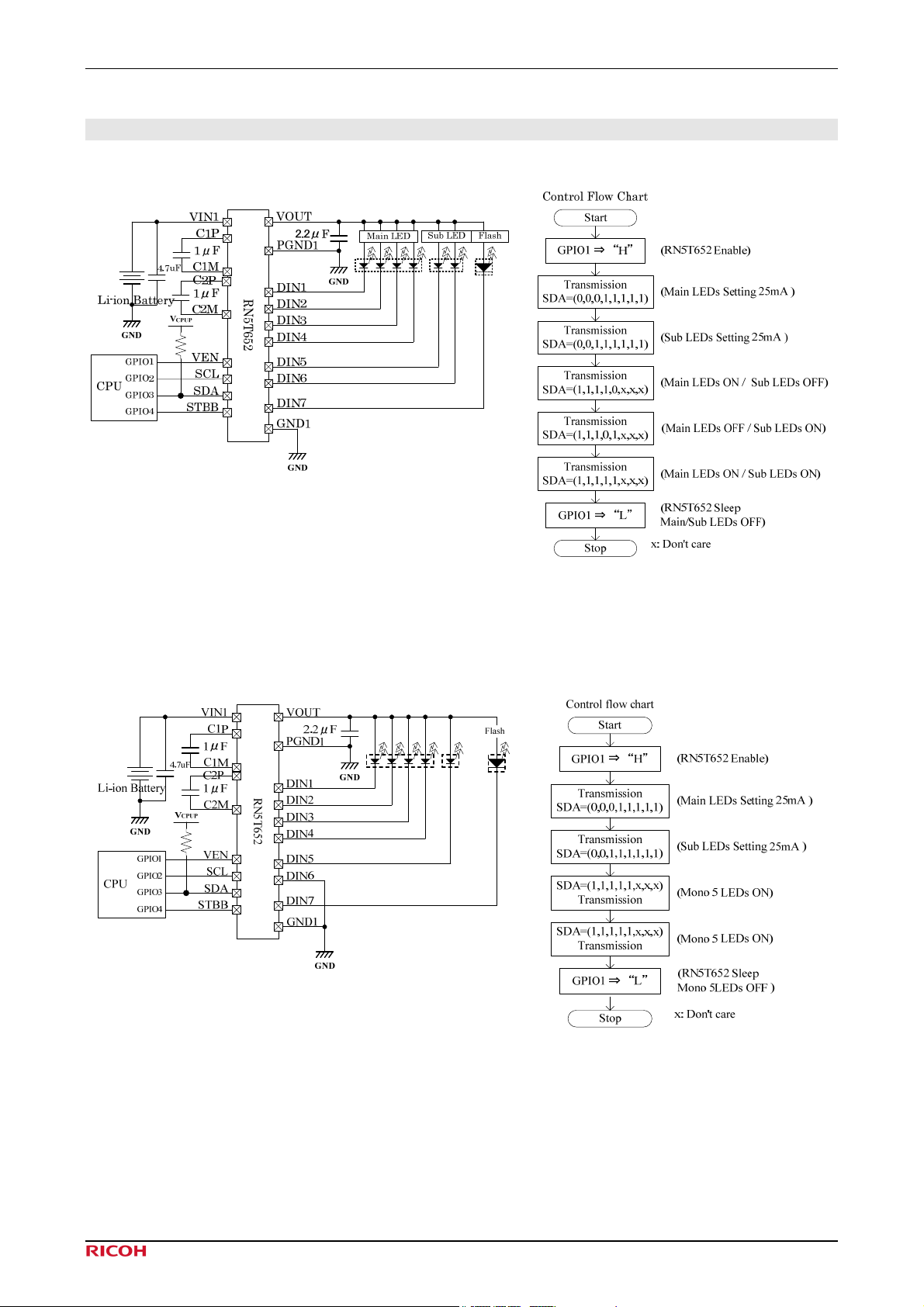
(1) Dual Main 4 LEDs and Sub 2 LEDs
(2) Mono 5 LEDs
Fig 9-1 Dual Main 4 LEDs and Sub 2 LEDs
Note*: Please connect DIN6 to GND.
Fig 9-2 Mono 5 LEDs
©2009 Rev. 1.5 Page 25
Page 27
RN5T652 Rev. 1.5
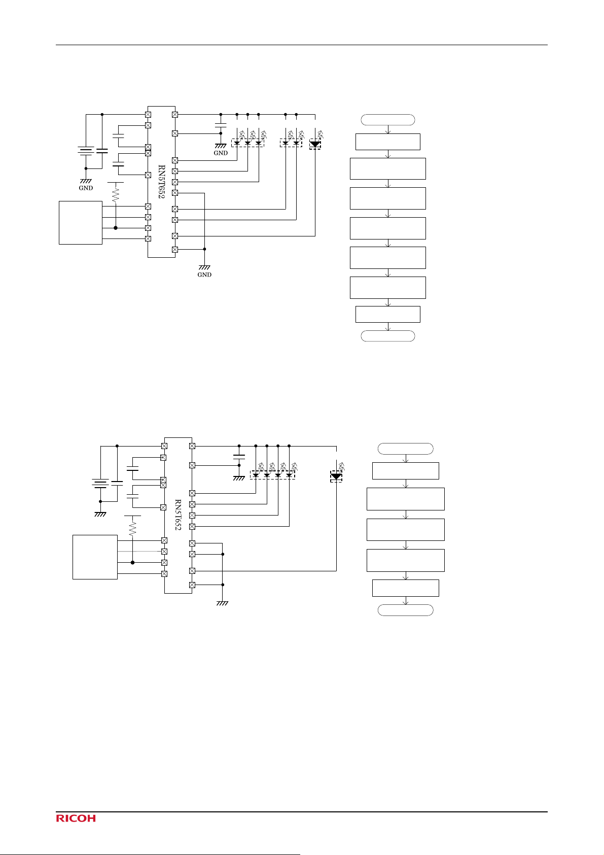
(3) Dual Main 3 LEDs and Sub 2 LEDs
VOUT
PGND1
DIN1
DIN2
DIN3
DIN4
DIN5
DIN6
DIN7
GND1
Li-ion Battery
GPIO1
GPIO2
CPU
GPIO3
GPIO4
VIN1
C1P
1μF
C1M
4.7uF
C2P
1μF
C2M
VCPUP
VEN
SCL
SDA
STBB
MONO 4 LEDs
Note*: Please connect DIN4 to GND.
2.2μF
Control flow chart
Main LED Sub LED Flash
Start
GPIO1 ⇒“H”
Transmission
SDA=(0,0,0,1,1,1,1,1)
Transmission
SDA=(0,0,1,1,1,1,1,1)
Transmission
SDA=(1,1,1,1,0,x,x,x)
Transmission
SDA=(1,1,1,0,1,x,x,x)
Transmission
SDA=(1,1,1,1,1,x,x,x)
GPIO1 ⇒“L”
Stop
Fig 9-3 Dual Main 3 LEDs and Sub 2 LEDs
(RN5T652 Enable)
(Main LEDs Setting 25mA )
(Sub LEDs Setting 25mA )
(Main LEDs ON / Sub LEDs OFF)
(Main LEDs OFF / Sub LEDs ON)
(Main LEDs ON / Sub LEDs ON)
(RN5T652 Sleep
Main/Sub LEDs OFF)
x: Don't care
(4) Mono 4 LEDs
Control flow chart
Start
GPIO1 ⇒“H”
Transmission
SDA=(0,0,0,1,1,1,1,1)
SDA=(1,1,1,1,0,x,x,x)
Transmission
SDA=(1,1,1,0,0,x,x,x)
Transmission
GPIO1 ⇒“L”
Stop
(RN5T652 Enable)
(Main LEDs Setting 25mA )
(Mono 4 LEDs ON)
(Mono 4 LEDs ON)
(RN5T652 Sleep
Mono 4 LEDs OFF )
x: Don't care
Li-ion Battery
GND
GPIO1
GPIO2
CPU
GPIO3
GPIO4
4.7uF
VCPUP
VIN1
C1P
1μF
C1M
C2P
1μF
C2M
VEN
SCL
SDA
STBB
VOUT
2.2μF
PGND1
DIN1
DIN2
DIN3
DIN4
DIN5
DIN6
DIN7
GND1
Flash
GND
GND
Note*: When DIN5 and 6 are not used, write “0” in D3 (Sub Enable) bit of the other function register always or
connect DIN5 and DIN6 to GND.
Fig 9-4 Mono 4 LEDs
©2009 Rev. 1.5 Page 26
Page 28
RN5T652 Rev. 1.5
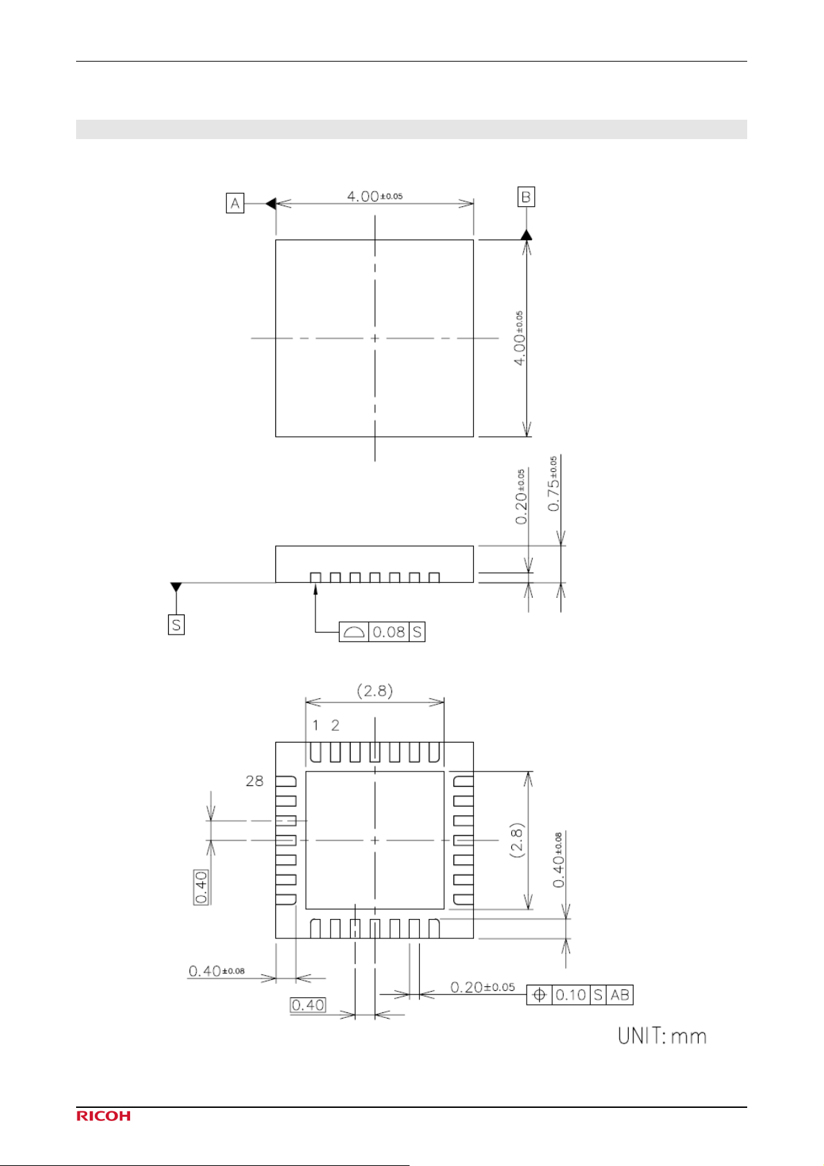
10. Package Information
©2009 Rev. 1.5 Page 27
 Loading...