

Page 1

Charge pump for White LED
RN5T649
Development Specifications
Rev. 1.2
2009/05/19
RICOH COMPANY, LTD.
Electronic Devices Company
This specification is subject to change without notice.
Page 2

RN5T649 CHARGE PUMP FOR WHITE LED
Table of Contents
1.
Outline........................................................................................................................................................................3
2. Feature .......................................................................................................................................................................3
3. Ordering Information ...............................................................................................................................................3
4. Pin Configuration......................................................................................................................................................4
5. Typical Application Circuit ......................................................................................................................................5
6. Pin Description ..........................................................................................................................................................6
7. Functional Blocks......................................................................................................................................................7
7.1 Single Wire Serial Pulse I/F of LDO1/2 .............................................................................................................7
7.2 LDO1/2 Electrical Characteristics ......................................................................................................................8
7.3 Charge Pump.......................................................................................................................................................9
7.3.1 Block Diagram ..........................................................................................................................................9
7.3.2 Backlight LED......................................................................................................................................... 10
7.3.3 Protection Circuit .................................................................................................................................... 11
7.3.4 Unused DIN_ pin ....................................................................................................................................11
7.3.5 Soft-start.................................................................................................................................................. 11
7.3.6 Luminance Control.................................................................................................................................. 12
7.3.7 Single Wire Serial Pulse I/F of LED Driver............................................................................................ 13
7.3.8 Charge Pump Electrical Characteristics .................................................................................................. 14
7.4 UVLO (Under Voltage Lock Out)....................................................................................................................15
7.5 Thermal Shutdown Circuit................................................................................................................................16
7.5.1 Thermal Shutdown Electrical Characteristics .........................................................................................16
8. Electrical Characteristics........................................................................................................................................17
8.1 Absolute Maximum Ratings .............................................................................................................................17
8.2 Recommendation of Operation Conditions.......................................................................................................17
8.3 DC Characteristics ............................................................................................................................................17
9. Package Information...............................................................................................................................................18
©2009 Rev. 1.2 Page 2
Page 3
CHARGE PUMP FOR WHITE LED RN5T649
1. Outline
RN5T649 contains a constant frequency charge pump, which is optimized for White LED application. Output
enable/disable, LEDs current and LDOs ON/OFF are individually controllable through single wire serial pulse I/F.
2. Feature
z White LED Charge Pump
9 Current capability: Up to 92mA
9 1x/1.33x/1.5x switchable charge pump mode
9 Power up four LEDs for backlight: Up to 23mA/LED
9 Luminance control with 32steps from 0.25mA to 23mA
9 Soft-start
z Power Supply Function
9 LDO (150mA) × 2 (ON/OFF control through single wire serial pulse I/F)
9 LDO output voltage is settable in 0.05V step in range of 1.2V to 3.3V
9 Over current protection (All Regulators) and thermal shutdown
z Others
9 UVLO
9 Short-circuit Protection
z Package
9 20pin QFN package (Body size: 3.0 x 3.0 x 0.75mm, Pin pitch 0.4mm)
z Process
9 CMOS process
3. Ordering Information
RN5T649
LDO Output voltage : LDOUT1 / LDOUT2
U: 1.80V / 2.80V
V: 1.50V / 2.80V
©2009 Rev. 1.2 Page 3
Page 4
CHARGE PUMP FOR WHITE LED RN5T649
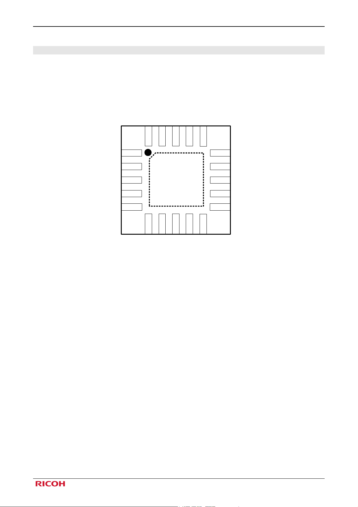
4. Pin Configuration
LDOCTL
20
DIN1
19
DIN2
18
NC
GNDCOM
17
16
LEDCTL
C2M
C3P
VOUT
C1P
1
2
3
TOP VIEW
4
5
6
7
C2P
C1M
9
8
C3M
VCCCP
Fig 4-1 Pin Configuration
10
GNDCP
15
14
13
12
11
DIN3
DIN4
LDOUT2
VCCCOM
LDOUT1
©2009 Rev. 1.2 Page 4
Page 5
CHARGE PUMP FOR WHITE LED RN5T649
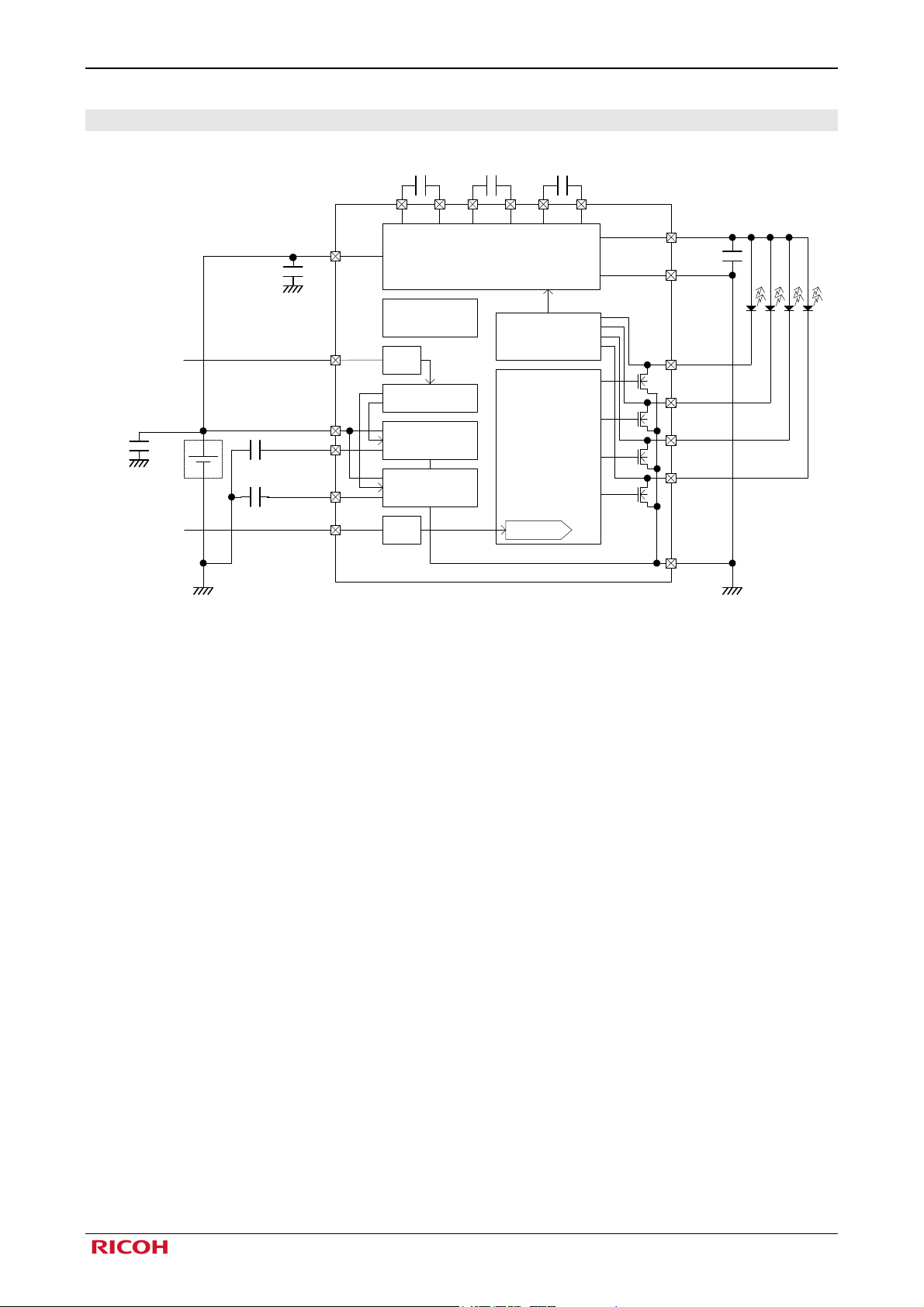
5. Typical Application Circuit
VCCCP
4.7uF
GND
Controlled with
GPIO of CPU
4.7uF
GND
Controlled with
GPIO of CPU
Li-ion
Battery
GND
LDOCTL
VCCCOM
1uF
LDOUT2
1uF
LEDCTL
NR: Noise reduction
1uF 1uF 1uF
Charge Pump
@92mA (1x,1.33x,1.5x)
Thermal
Shutdown
NR
Logic
LDO1LDOUT1
LDO2
NR
RN5T649
Feed Back
Adjust Voltage
Current Driver
5bit DAC
VOUT
2.2µF
GNDCP
DIN1
@23mA
DIN2
@23mA
DIN3
@23mA
DIN4
@23mA
GNDCOM
GND
Fig 5-1 Typical Application Circuit
©2009 Rev. 1.2 Page 5
Page 6
RN5T649 CHARGE PUMP FOR WHITE LED
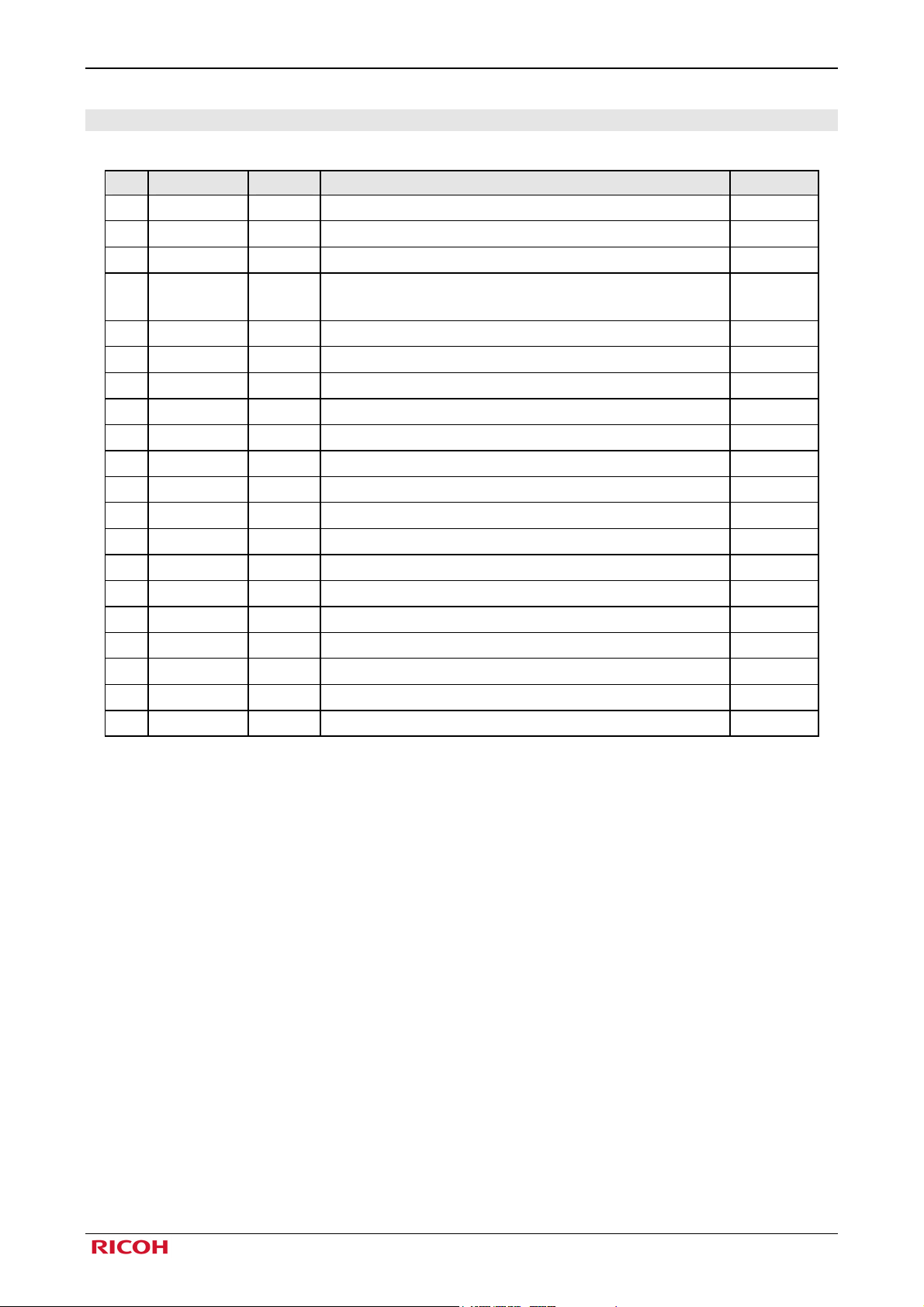
6. Pin Description
No. Name I/O Description Notes
LEDCTL
1
2
3
4
5
6
7
8 VCCCP PWR Power supply for charge pump
9
10
11
12
13
14
15
16
17
18
19
20
C2M
C3P
VOUT
C1P
C2P
C1M
C3M
GNDCP
LDOUT1
VCCCOM
LDOUT2
DIN4
DIN3
NC
GNDCOM
DIN2
DIN1
LDOCTL
I ON/OFF control and Current setting of LED driver
- Charge pump boost capacitor connection
- Charge pump boost capacitor connection
O
GND Ground for charge pump
O Output of LDO1.
PWR Power supply for LDO, UVLO, Logic block and TSHUT.
O Output of LDO2
O LED driver current control output
O LED driver current control output
GND Ground for LDO, UVLO, Logic block and TSHUT.
O LED driver current control output
O LED driver current control output
LED driver voltage output.
VOUT is high impedance during shutdown.
- Charge pump boost capacitor connection
- Charge pump boost capacitor connection
- Charge pump boost capacitor connection
- Charge pump boost capacitor connection
- No connection *1
I LDO1/2 ON/OFF control input
Note*1: NC pin should be connected to GND or open.
Table 6-1 Pin Description
©2009 Rev. 1.2 Page 6
Page 7
CHARGE PUMP FOR WHITE LED RN5T649
7. Functional Blocks
7.1 Single Wire Serial Pulse I/F of LDO1/2
RN5T649 has 2 Low Drop Output regulators, LDO1 and LDO2. At time of shipment, the output voltage can be set in
0.05 V steps by trimming.
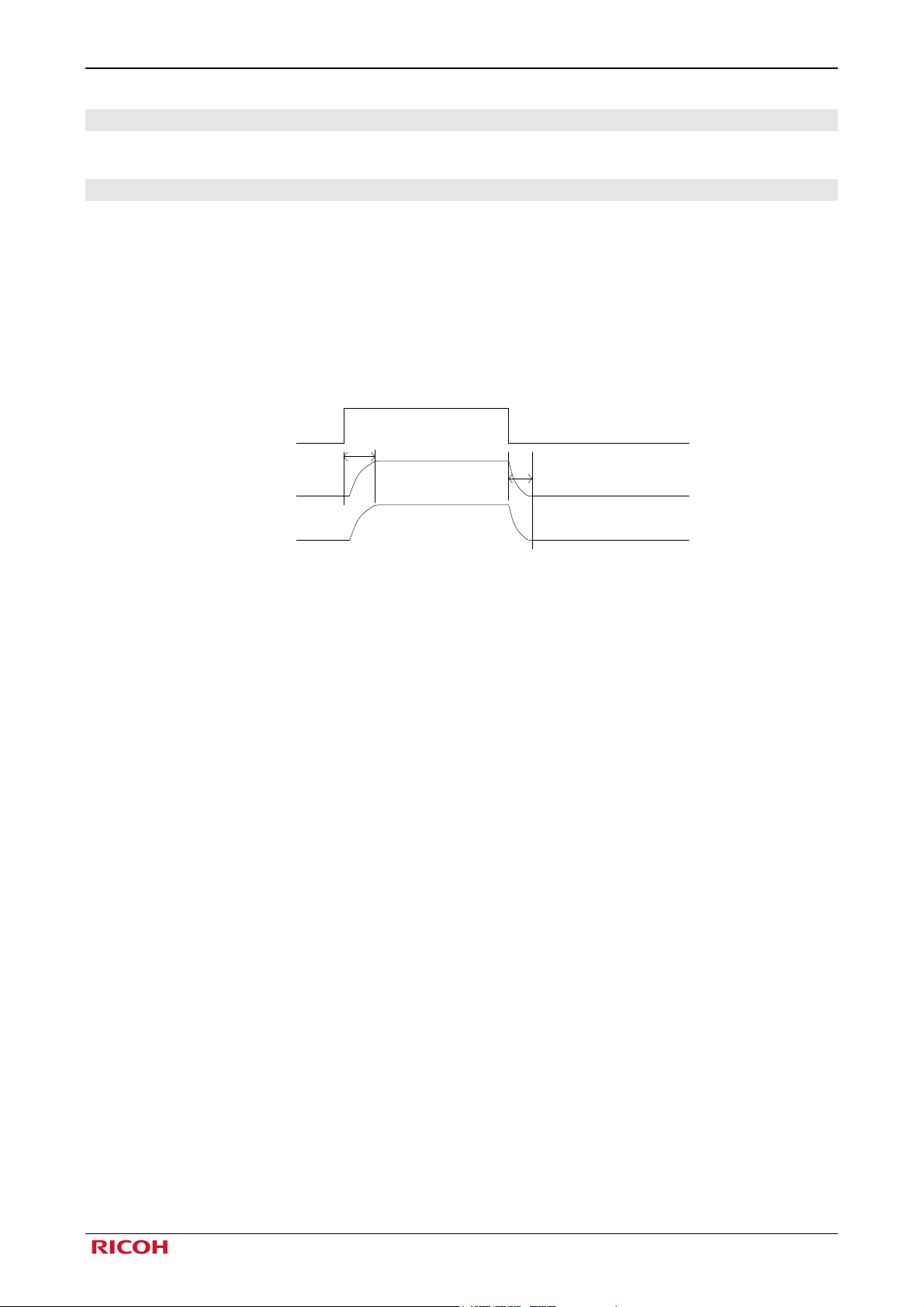
ON/OFF operation of LDO1 and LDO2 is controllable with LDOCTL pin through single wire serial pulse I/F.
Please refer to the following timing chart. LDO1 and LDO2 are turned on after t
OUT (=20us typ) when LDOCTL
changes from “L” to “H”.
LDOCTL
LDO1
LDO2
t
tHI>10us
OUT
tOUT≒20us (typ)
tOFF≒70us (typ)
tLO>10us
tOFF
Fig 7-1 LDO ON/OFF Control 1
For the type of the bypass capacitor, it must be a ceramic type, not tantalum type, since the optimization design is based
on the ceramic type for the phase compensation.
*Timer description
・tOUT : If LDOCTL remains “H” more than 10us, the voltage appears to both LDOUT1 pin and LDOUT2 pin.
・tOFF : “L” pulse of LDOCTL pin more than 10us turns off both LDO1 and 2.
©2009 Rev. 1.2 Page 7
Page 8
RN5T649 CHARGE PUMP FOR WHITE LED
7.2 LDO1/2 Electrical Characteristics
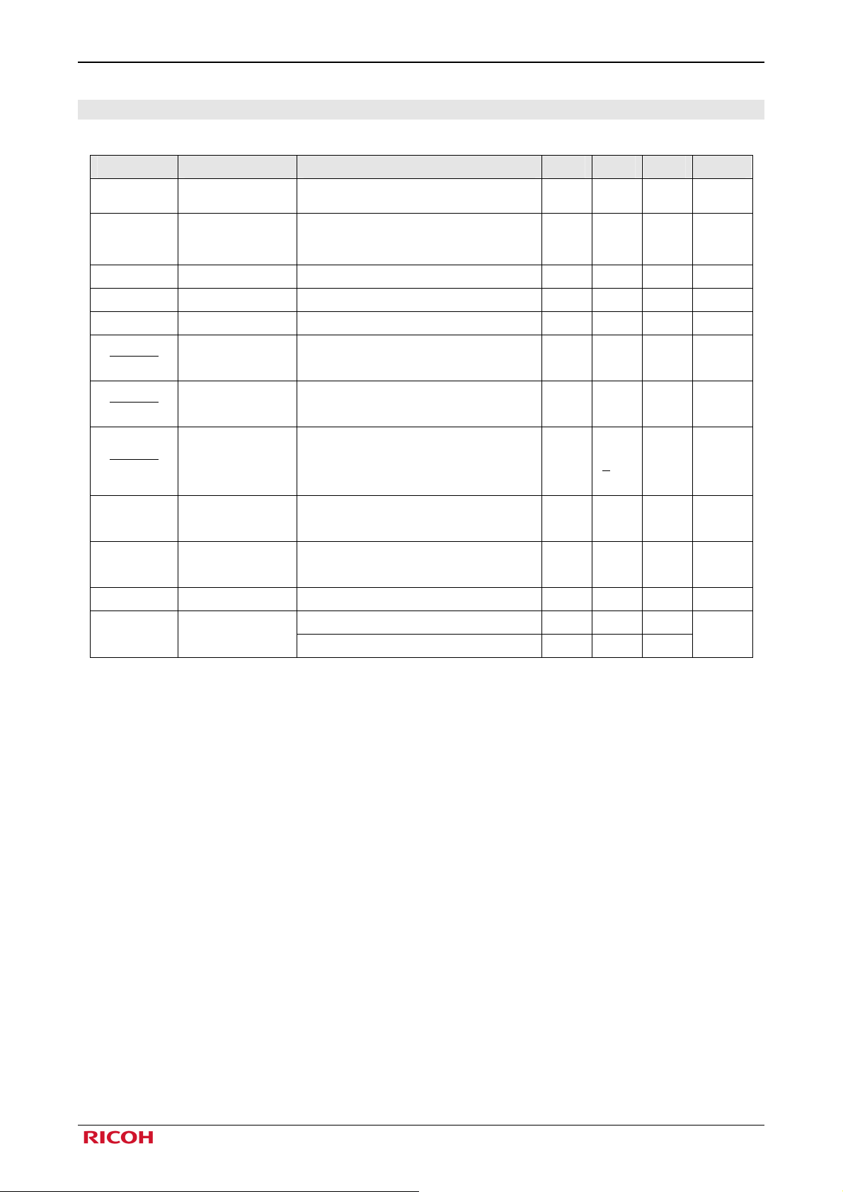
Unless otherwise specified, VCCCOM=3.6V, Ta=25℃, Cout=1.0uF
Symbol Parameter Condition Min Typ Max Units
LDOUT*1
VACC
Range
Output Voltage
Accuracy
50uA<IOUT<150mA,
VOUT+0.5V≦V
& 3.0V≦V
IOUT Output Current - 150 mA
ISHT Short Current VOUT=0V 130 mA
Output Voltage
VDRP Drop-out Voltage
ΔVOUT
Line Regulation
IOUT=150mA,T
VOUT+0.5V≦VCCCOM≦4.5V
ΔVCCCOM
ΔVOUT
Load Regulation
50uA<IOUT<150mA
ΔIOUT
ΔVOUT
ΔT
a
RR Ripple Rejection
EN
BC *2 Bypass Capacitor
Icc
Output Voltage
Temperature
Coefficient
Output Noise
(RMS)
Consumption
-40℃≦T
f=10Hz-10kHz, C
BW=100Hz-100kHz, C
0uA<IOUT<150mA
Normal (IOUT=0mA) 70
Current
- 1.2 3.3 V
(VCCCOM)
BATT
(VCCCOM)≦4.5V
BATT
=85℃,VOUT≧2.8V
a
-2% +2% V
300 mV
2.4 mV
IOUT=150mA
25 mV
≦85℃
a
out
=1.0uF
+
60 dB
100
IOUT=75mA
=1.0uF
out
IOUT=75mA
50 uVrms
1.0 uF
OFF 1
ppm/℃
uA
Table 7-1 LDO1/2 Electrical Characteristics
Note*1: The output voltage will be fixed (in 0.05V step) by trimming at shipment.
Note*2: For optimized phase compensation, the bypass capacitor must be a ceramic type.
©2009 Rev. 1.2 Page 8
Page 9

CHARGE PUMP FOR WHITE LED RN5T649
7.3 Charge Pump
RN5T649 drives up to 4 white LEDs with regulated constant current. Utilizing 1x/1.33x/1.5x charge pump modes
achieves high-efficiency. On/off of LED is individually controllable through single wire serial pulse I/F. Also, the
luminance of LED is individually controllable through single wire serial pulse I/F.
The capacitor is highly recommended to be ceramic.
7.3.1 Block Diagram
VCCCP
LEDCTL
NR: Noise reduction
1uF
C1M
C1P
C2M
1uF
Charge Pump
@92mA( 1x,1.33x,1.5x)
Thermal
Shutdown
NR
1uF
C2P
C3M
Feed Back
Adjust Voltage
Current Driver
5bit DAC
C3P
VOUT
2.2µF
GNDCP
DIN1
@23mA
DIN2
@23mA
DIN3
@23mA
DIN4
@23mA
GNDCOM
GND
Fig 7-2 Charge Pump Circuit Diagram
©2009 Rev. 1.2 Page 9
Page 10
CHARGE PUMP FOR WHITE LED RN5T649
7.3.2 Backlight LED
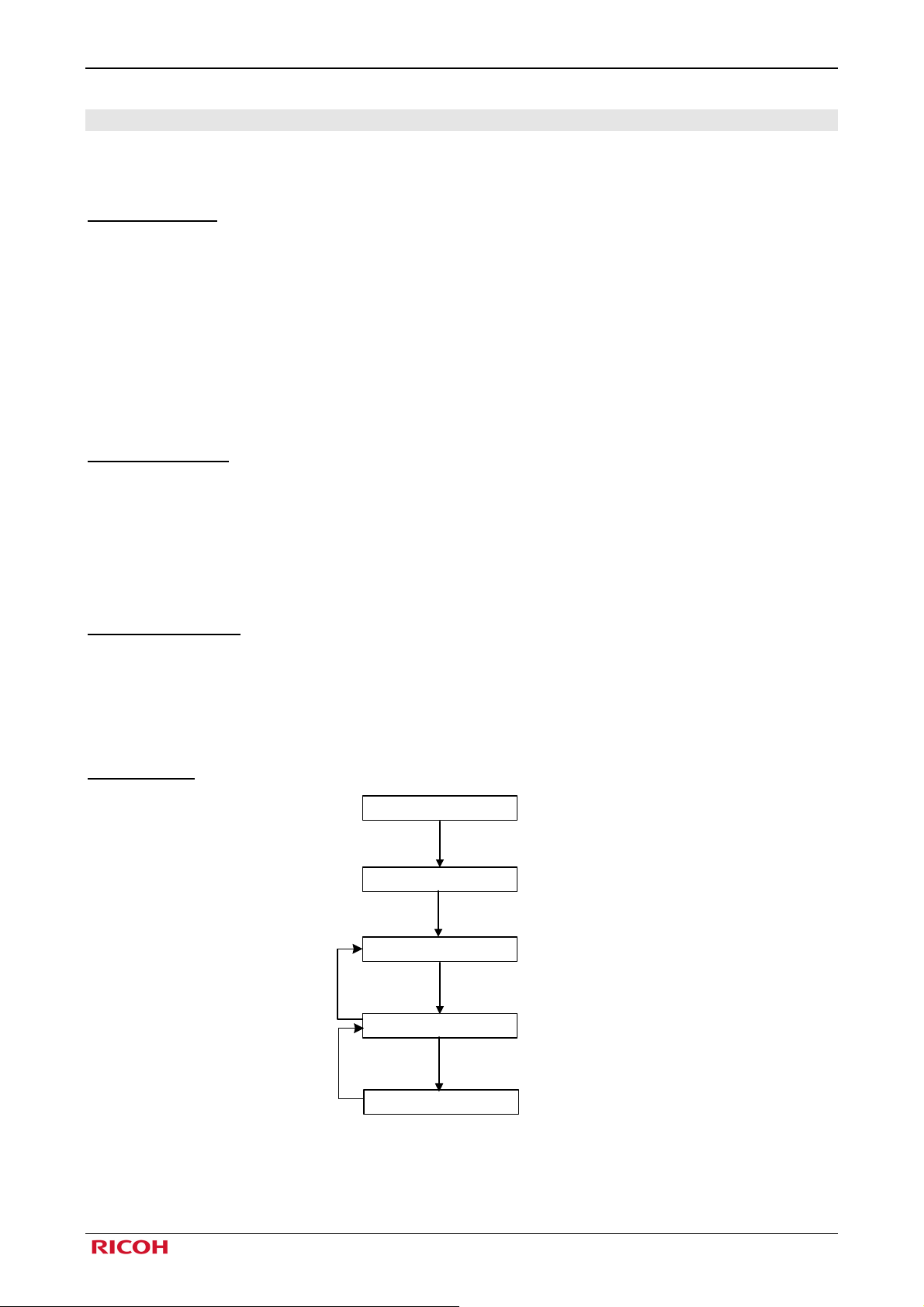
For maximized power efficiency, Charge pump operates 1x mode, 1.33x mode and 1.5x mode, where the operation
mode is determined by comparing the forward voltage of each LED with the input voltage.
Initial and 1x mode
When any LED channel is enabled and VCCCP voltage is greater than Charge pump output (VOUT), Charge pump
initially starts in 1x mode and VOUT is pulled up to VCCCP. During start-up, built-in Soft-start circuitry will prevent
excessive inrush current. Charge pump circuit will stay in 1x mode if:
VOUT - Vf > 230mV (1)
VOUT: Charge pump output
Vf: White LED forward voltage
230mV: Mode transition threshold voltage when LED output current is set at 23mA.
1x or 1.33x transition
When VCCCP falls and DIN_ pin voltage drops below the mode transition threshold voltage 230mV for 100us, Charge
pump circuit switches to 1.33x mode to boost voltage. Charge pump circuit will stay in 1.33x mode if:
VOUT - Vf > 230mV (2)
Every 1sec, Charge pump circuit resets to 1x mode and stays in 1x mode for approximately 100us to judge whether it
changes to 1.33x mode or stays in 1x mode.
1.33x or 1.5x transition
When VCCCP falls and DIN_ pin voltage drops further below the mode transition threshold voltage 230mV for 100us,
Charge pump circuit switches to 1.5x mode to boost voltage.
Every 1sec, Charge pump circuit resets to 1.33x mode and stays in 1.33x mode for approximately 100us to judge
whether it changes to 1.5x mode or stays in 1.33x mode.
Mode transition
Reset to 1x mode
Reset to 1.33x
mode every sec
every sec
Initial
LED channel enabled
VOUT soft start
VOUT pulled up to VCCCP
1x Mode, LED On
Min. DIN_ lower than 230mV.
1.33x Mode
Min. DIN_ lower than 230mV.
1.5x Mode
VOUT = GND
VOUT = VCCCP-Ro*Iled
DIN_=VOUT-Vf
VOUT = 1.33*VCCCP-Ro*Iled
DIN_=VOUT-Vf
VOUT = 1.5*VCCCP-Ro*Iled
DIN_=VOUT-Vf
Ro:Output Resistanse
Iled:DIN1-4 LED current
Fig 7-3 Mode Transition Diagram
©2009 Rev. 1.2 Page 10
Page 11
CHARGE PUMP FOR WHITE LED RN5T649
7.3.3 Protection Circuit
When any DIN_ pin is floating or grounded, VOUT voltage is limited below protection voltage by gating on/off charge
pump. In case any LED fails as an open circuit, VOUT voltage is also limited. Besides, when VOUT is smaller than
approximately 1.2V, Charge pump will stop.
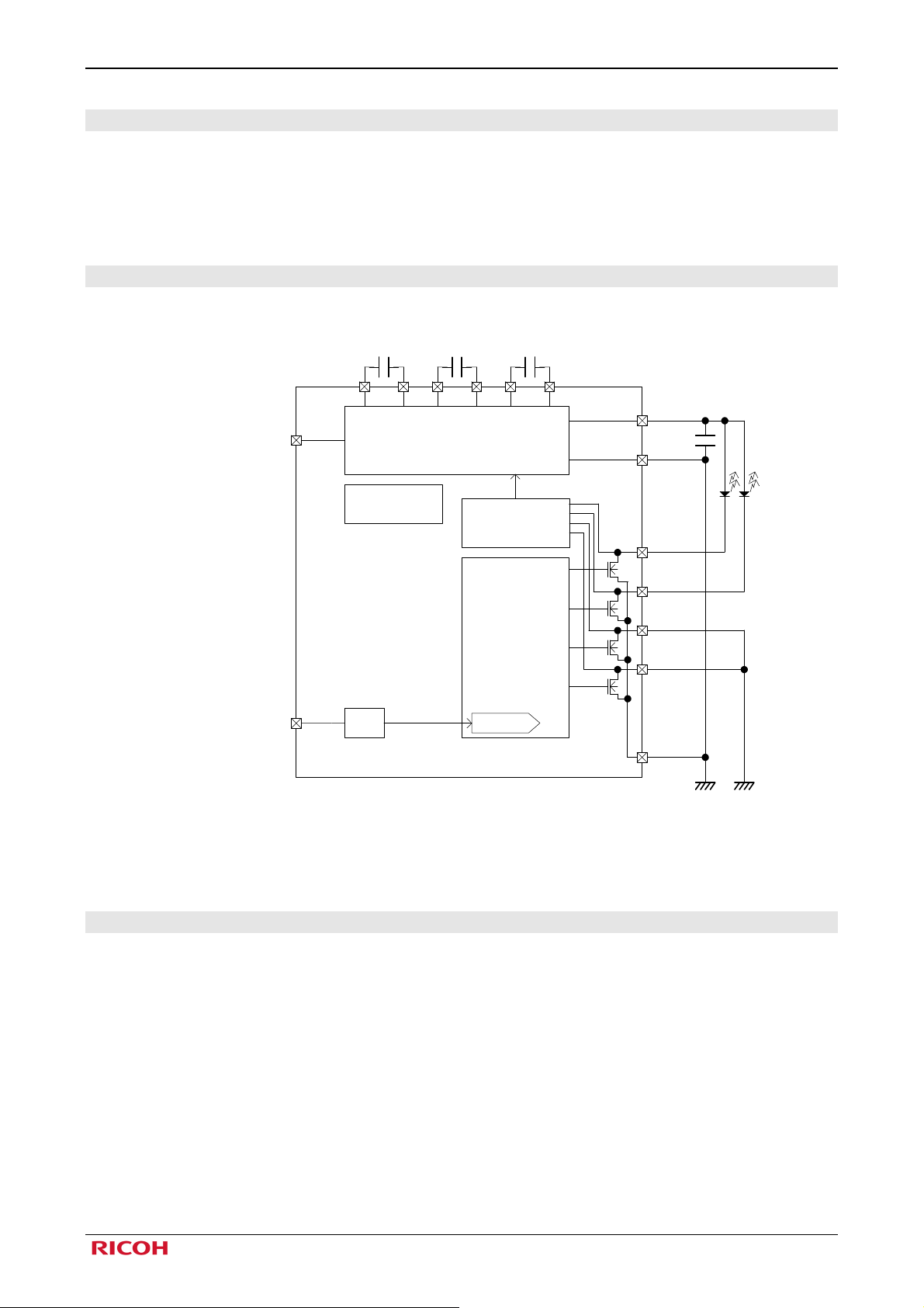
7.3.4 Unused DIN_ pin
Please ground unused DIN_ pin to avoid over-voltage protection status.
VCCCP
LEDCTL
1uF
C1M
Shutdown
NR
NR: Noise reduction
C1P
Charge Pump
@92mA (1x,1.33x,1.5x)
Thermal
1uF
C2M
1uF
C2P
C3M
Feed Back
Adjust Voltage
Current Driver
5bit DAC
C3P
VOUT
2.2µF
GNDCP
DIN1
@23mA
DIN2
@23mA
DIN3
DIN4
GNDCOM
GND
GND
Fig 7-4 Ground Unused DIN_pin
7.3.5 Soft-start
RN5T649 includes Soft-start circuitry to prevent excessive inrush current during turn on. (The internal resistance
gradually increases, just after LEDs enabled.)
When charge pump turns on, the capacitors are charged directly from input voltage. Soft-start is achieved by the amount
of capacitor available to capacitor for approximately 100us.
©2009 Rev. 1.2 Page 11
Page 12
CHARGE PUMP FOR WHITE LED RN5T649
7.3.6 Luminance Control
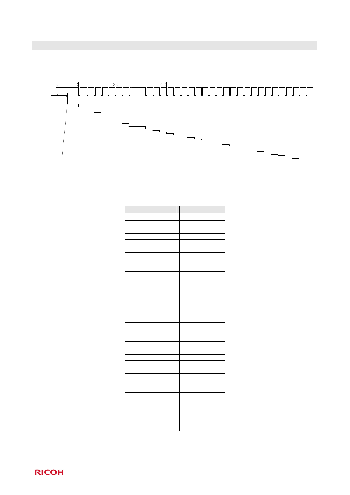
RN5T649 charge pump drives 4 LEDs with regulated constant current for uniformed intensity. LEDCTL input
enables/disables LED and adjusts current for each LED with 32 steps from 0.25mA to 23mA.
14.5
tHI > 2.8us
13
12.5
18 19 20 21 22 23 24 25 26 27 28 29 3 0 31 32
11
10
9
8.5
8
7
6.5
6
5.5
5
4.5
4
3.5
3
2.5
2
1.5
1
23
0.5
0.25
LEDCTL
MLED
I
INITIAL tHI > 300µs
Soft-start
23
tLO 2.8us to 250µs
1 2 345678 91011121314151617
22
20
19.5
19
18
17
16
15
Fig 7-5 Luminance Control Diagram
・tHI : Pulling LEDCTL pin “H” for 300us or more enables LED. The minimum “H” time of LEDCTL pin is 2.8us.
・tOFF : “L” pulse of LEDCTL pin longer than 1ms turns off LED.
Luminance Count value
OFF⇒ON(23mA)
22mA 1 (01h)
20mA 2 (02h)
19.5mA 3 (03h)
19mA 4 (04h)
18mA 5 (05h)
17mA 6 (06h)
16mA 7 (07h)
15mA 8 (08h)
14.5mA 9 (09h)
13mA 10 (0Ah)
12.5mA 11 (0Bh)
11mA 12 (0Ch)
10mA 13 (0Dh)
9mA 14 (0Eh)
8.5mA 15 (0Fh)
8mA 16 (10h)
7mA 17 (11h)
6.5mA 18 (12h)
6mA 19 (13h)
5.5mA 20 (14h)
5mA 21 (15h)
4.5mA 22 (16h)
4mA 23 (17h)
3.5mA 24 (18h)
3mA 25 (19h)
2.5mA 26 (1Ah)
2mA 27 (1Bh)
1.5mA 28 (1Ch)
1mA 29 (1Dh)
0.5mA 30 (1Eh)
0.25mA 31 (1Fh)
23mA 32 (20h)
… …
0 (00h)
Table 7-2 LED Luminance Control
©2009 Rev. 1.2 Page 12
Page 13
CHARGE PUMP FOR WHITE LED RN5T649
7.3.7 Single Wire Serial Pulse I/F of LED Driver
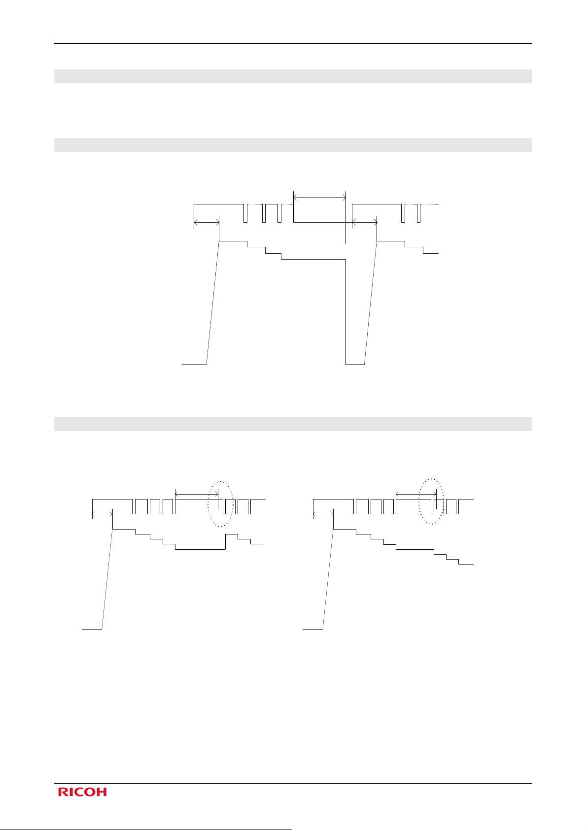
When LEDCTL goes high, LEDs are enabled at full luminance. After, the subsequent low going pulse reduces LED
current in linear (1.0mA or 0.5mA) scale.
7.3.7.1 Disable LED
LED can be powered off by driving LEDCTL pin low longer than tOFF.
tOFF
2ms (typ)
LEDCTL
Soft-start
1 2 34 12
23
22
20
19.5
Soft-start
23
22
20
I
LED
Fig 7-6 Disable LED
7.3.7.2 Initialization of LED
Luminance can be adjusted to initial value by driving LEDCTL pin “H” longer than tRESET
remains power-on.)
LEDCTL
I
LED
Soft-start
tRESET
2ms (typ) 2ms (typ)
23
22
20
19.5
19
1 51 2 34 23
22
20
19.5
LEDCTL
I
LED
Soft-start
1 2 34 67
23
22
tRESET
20
19.5
19
but not over tOFF. (LED
18
17
16
Fig 7-7 Initialization of LED
* Timer description
・tRESET timer starts at falling edge of the input clock from LEDCTL and is cleared at rising edge of input clock from
LEDCTL.
・tOFF timer starts at rising/falling edge of the input clock from LEDCTL and turns off when timer overflows.
©2009 Rev. 1.2 Page 13
Page 14
RN5T649 CHARGE PUMP FOR WHITE LED
7.3.8 Charge Pump Electrical Characteristics
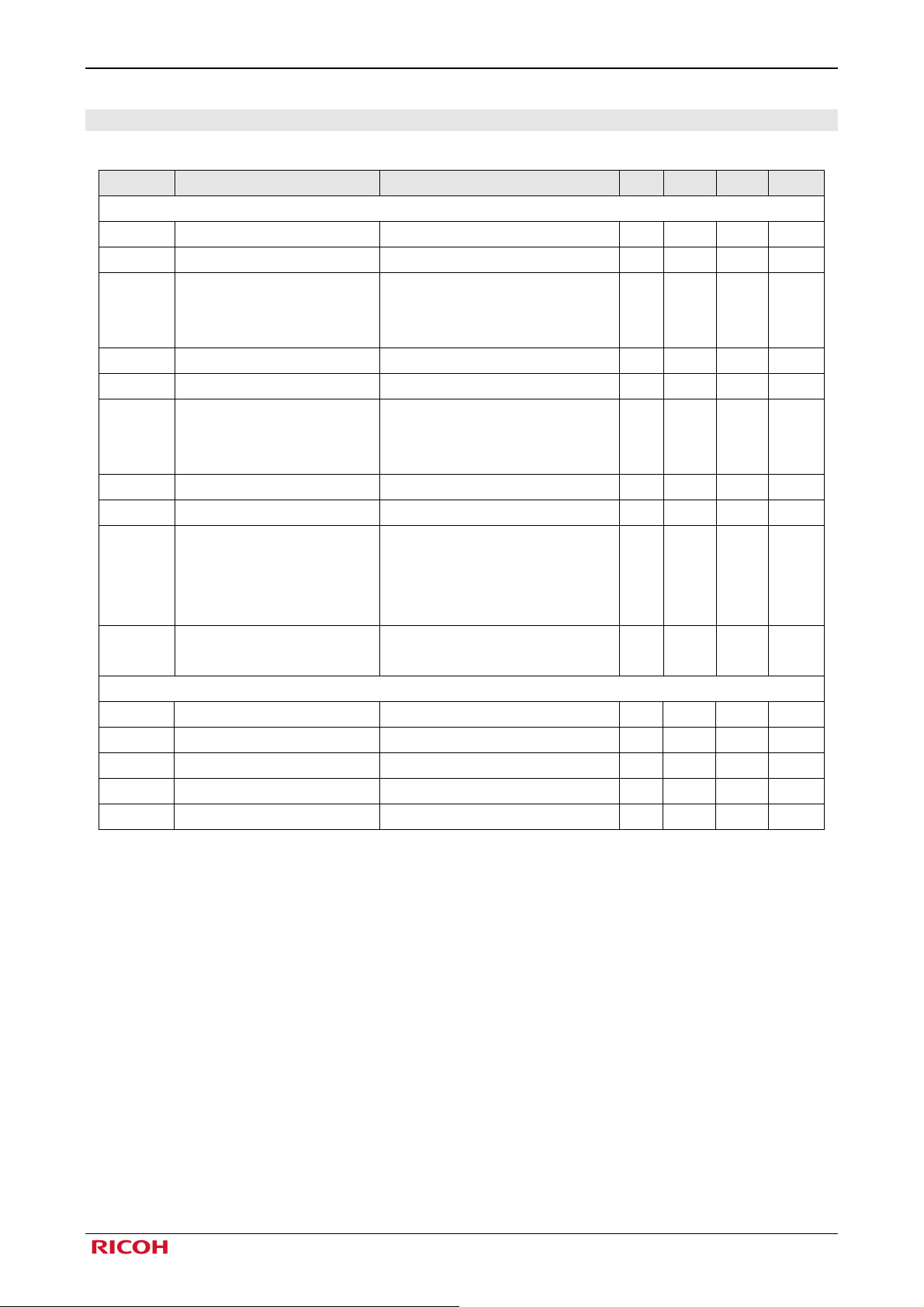
Unless otherwise specified, VCCCP=3.6V, VCCCOM=3.6V, Ta=25℃, C1=C2=C3=1uF, Cout=2.2uF
Symbol Parameter Condition Min Typ Max Units
Charge Pump
VIN Operating Voltage VCCCP voltage 3.0 4.5 V
I
Max. Output current
OUT
RON Output resistance
1.33x : (1.33xVCCCP-Vout)/Iout
1.5x : (1.5xVCCCP-Vout)/Iout
F
Switching Frequency - 1.0 MHz
OSC
T
Soft-start time - 100 us
SOFT
Icc Consumption Current
VCCCP≧3.0V
1x : (VCCCP-Vout)/Iout
1x mode
1.33X mode
1.5x mode
92 mA
0.8
3.2
Ω
5.8
1
5
mA
5
Iss Standby consumption current VCCCP current 5 uA
I
Current limit VOUT shorted 120 mA
LIM
1x to 1.33x transition
V
TH1
threshold
1.33x to 1.5x transition
- 230 mV
threshold
V
TIM
1x to 1.3x transition time
1.33x to 1.5x transition time
- 100 us
LED Driver
Isink Maximum Sink Current Each DIN1-4 23 mA
ACC LED current accuracy Setting DATA Max , DIN*=0.23V -5 5 %
I
*1 LED current matching Setting DATA Max ,Vfdiff<0.4V -2 2 %
MAT
V
Current Regulator Dropout Setting DATA Max 230 mV
Drop
I
DIN1-4 leakage in shutdown - 0.01 uA
LEAK
Table 7-3 Charge Pump Electrical Characteristics
Note*1: The matching is given by (Iave - Iled ) / Iave. The Iave means the average current of 4 LEDs.
The matching is defined without Vf voltage difference between channels.
Iave = (Iled1 + Iled2 + Iled3 + Iled4 ) / 4
©2009 Rev. 1.2 Page 14
Page 15
RN5T649 CHARGE PUMP FOR WHITE LED
7.4 UVLO (Under Voltage Lock Out)
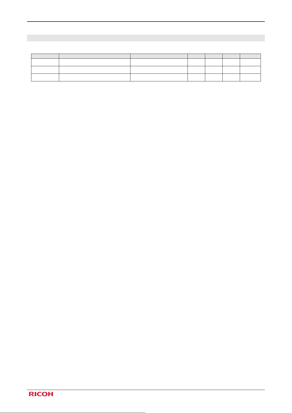
Unless otherwise specified, Ta=25℃
Symbol Parameter Condition Min Typ Max Units
V
Under voltage lock out threshold VCCVIN rising 2.25 V
Release
V
Under voltage lock out threshold VCCVIN falling 2.05 2.20 2.35 V
Detect
V
UVLO Hysteresis - 50 mV
HYS
Table 7-4 UVLO Electrical Characteristics
©2009 Rev. 1.2 Page 15
Page 16
RN5T649 CHARGE PUMP FOR WHITE LED
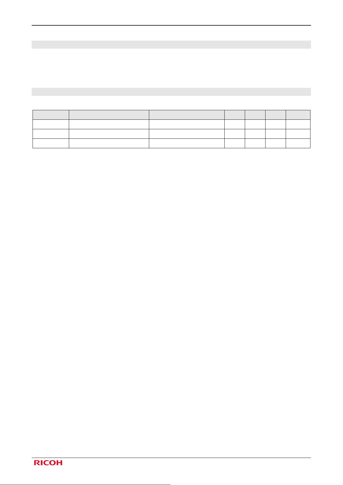
7.5 Thermal Shutdown Circuit
Overheat state can be detected by comparing the output voltages from two temperature detection circuits, which have
different temperature characteristics. If the overheat state is detected, RN5T649 will turn off to protect itself from
overheating.
7.5.1 Thermal Shutdown Electrical Characteristics
Unless otherwise specified, VCCCOM=3.6V, Ta=25℃
Symbol Parameter Condition Min Typ Max Units
T
Detected Temperature - 140
DET
T
Return Temperature - 110
RET
Icc Consumption Current - 10 uA
Table 7-5 Thermal Shutdown Electrical Characteristics
℃
℃
©2009 Rev. 1.2 Page 16
Page 17
RN5T649 CHARGE PUMP FOR WHITE LED
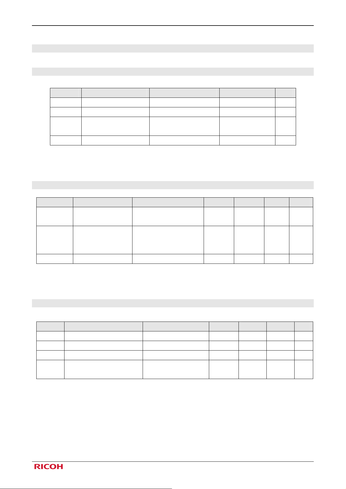
8. Electrical Characteristics
8.1 Absolute Maximum Ratings
Symbol Parameter Condition Rated value Units
VCC_abs Power Supply Voltage Battery Voltage Input Pins
Vin Input Voltage Range All Input Pins
PD
Package
Allowable Dissipation
T
Storage Temperature -
stg
Mounted on Board,
=70℃
T
a
Table 8-1 Absolute Maximum Ratings
8.2 Recommendation of Operation Conditions
Symbol Parameter Condition Min Typ Max Units
VCC_Op Power Supply Voltage
VCC_Rec Power Supply Voltage
Ta Temp. of Operation - -40 85
Battery Voltage Input Pins
(Operation Conditions)
Battery Voltage Input Pins
(Recommendation of
Operation Conditions)
2.7 3.6 4.5 V
3.0 3.6 4.5 V
-0.3~6.0
-0.3~VCC*+0.3
950 mW
-55~+125 ℃
V
V
℃
Table 8-2 Recommendation of Operation Conditions
8.3 DC Characteristics
Unless otherwise specified, VCCCOM=3.6V, Ta=25℃
Symbol Parameter Condition Min Typ Max Units
Vih “H” Input Voltage - 1.6 V
Vil “L” Input Voltage - 0.4 V
I
Input Leakage Current 1 VCCCOM -3 3 uA
IL1
Ishut
Shutdown Consumption
Current
LDOCTL=LEDCTL=“L” 1 uA
Table 8-3 DC Characteristics
©2009 Rev. 1.2 Page 17
Page 18

CHARGE PUMP FOR WHITE LED RN5T649
9. Package Information
©2009 Rev. 1.2 Page 18
 Loading...