

Page 1
VFM STEP-UP DC/DC
CONVERTER CONTROLLER
RN5RY202
NO.EA-042-0006
1
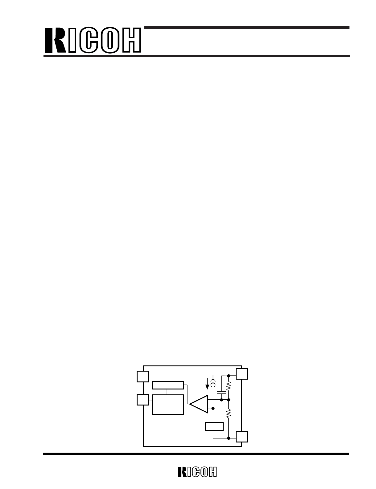
OUTLINE
The RN5RY202 Series are VFM (chopper) Control ICs for step-up DC/DC converter with an external power transis-
tor featuring high output voltage accuracy and low supply current by CMOS process. Each of the RN5RY202
Series ICs consists of a voltage reference unit, an error amplifier, an oscillator, a VFM control circuit and feed back
resistors.
Output voltage is fixed at 2V in the IC.
A low ripple, high efficiency step-up DC/DC converter can be constructed by simply adding an inductor, a diode, a
capacitor, and a drive transistor and feed back resistors.
Although the series have no CE pins unlike RN5RY
××1A, high voltage (VOUT=30V) can be also output by using
external feed back resistors.
FEATURES
• Low Supply Current
............................................................................
TYP. 3µA
• Low Temperature-Drift Coefficient of Output Voltage
...................
TYP. ±50ppm/˚C
• High Accuracy Output Voltage
.........................................................
±2.5%
• Low Oscillation Start-up Voltage (no load)
......................................
MAX. 0.8V
• Any output voltage can be set with external resistors
• Small Package SOT-23-5 (Mini-Mold)
APPLICATIONS
• Constant voltage power source for battery-powered instruments.
• Constant power source for cameras, camcorders, pagers, and other hand-held communication tools.
• Constant power source for devices that require higher voltages than battery voltages.
BLOCK DIAGRAM
+
–
2
3
1
5
Vref
Oscillator
Output
Buffer
VOUT
VDD
GND
EXT
Page 2
RN5RY202
2
SELECTION GUIDE
In the RN5RY202 Series, the taping type for the ICs can be selected at the user's request.
These selections can be made by designating the part number as shown below:
RN5RY202
×– ×× ←Part Number
↑↑↑ ↑
ab c d
{
{
Code Contents
a
20. Designation of Output Voltage (V
OUT)
V
OUT is fixed at 2.0V.
b2
Designation of Packing Type :
c A : Taping
C : Antistatic bag (for Samples only)
d
Designation of Taping Type :
Ex. TR, TL (refer to Taping Specifications ; TR type is prescribed as a standard.)
For example, Taping Type TR, is designated by Part Number RN5RY202A-TR.
PIN CONFIGURATION
• SOT-23-5
12
3
54
mark side
Page 3
RN5RY202
3
PIN DESCRIPTION
Pin No. Symbol Description
1 GND Ground Pin
2VDD Input Pin
3 EXT External Transistor Drive Pin (CMOS Output)
4 NC No Connection
5V
OUT Internal Voltage Output Pin (fixed at 2V)
ABSOLUTE MAXIMUM RATINGS
Symbol Item Ratings Unit
VDD Input Voltage 12 V
VOUT Output Pin Voltage 12 V
VEXT EXT Pin Output Voltage –0.3 to VDD+0.3 V
IEXT EXT Pin Output Current ±50 mA
PD Power Dissipation 150 mW
Topt Operating Temperature –40 to +85 ˚C
Tstg Storage Temperature –55 to +125 ˚C
Tsolder Lead Temperature (Soldering) 260˚C 10s (Lead part)
ABSOLUTE MAXIMUM RATINGS
Absolute Maximum ratings are threshold limit values that must not be exceeded even for an instant under
any conditions. Moreover, such values for any two items must not be reached simultaneously. Operation
above these absolute maximum ratings may cause degradation or permanent damage to the device. These
are stress ratings only and do not necessarily imply functional operation below these limits.
Page 4

RN5RY202
4
ELECTRICAL CHARACTERISTICS
• RN5RY202
Symbol Item Conditions MIN. TYP. MAX. Unit
VOUT Output Voltage VIN=VDD=1.9V 1.950 2.000 2.050 V
VIN Input Voltage 10 V
I
DD1 Supply Current 1
EXT No load, V
DD=1.9V
15 25 µA
VOUT=1.9V, Test circuits1
IDD2 Supply Curren 2
EXT No load, V
DD=1.9V
35µA
VOUT=2.1V, Test circuits1
fosc Maximum Oscillator Frequency
V
DD=1.9V, VOUT=1.9V
180 kHz
Test circuits2
Duty Oscillator Duty Cycle
V
DD=1.9V, VOUT=1.9V
65 75 %
EXT “H” side, Test circuits2
Vstart Oscillator Start-up Voltage EXT No load, Test circuits2 0.7 0.8 v
∆V
OUT Output Voltage IOUT=10mA
±50 ppm/˚C
∆Topt Temperature Coefficient –40˚C≤Topt≤85˚C
I
EXTH EXT “H” Output Current
V
DD=1.9V, VOUT=1.9V
–1.5 mA
VEXT=GND, Test circuits3
IEXTL EXT “L” Output Current
V
DD=1.9V, VOUT=1.9V
1.5 mA
VEXT=1.9V, Test circuits4
R
VSET Voltage Set Resistor
V
DD=2V, VOUT=10V
2MΩ
Test circuits5
Topt=25˚C
Page 5

RN5RY202
5
TEST CIRCUIT
A
A
A
Oscilloscope
GND
V
DD
EXT
NC
V
OUT
Oscilloscope
Oscilloscope
GND
V
DD
EXT
NC
V
OUT
GND
V
DD
EXT
NC
V
OUT
GND
V
DD
EXT
NC
V
OUT
GND
V
DD
EXT
NC
V
OUT
Test Circuit1
Test Circuit4
Test Circuit2
Test Circuit5
Test Circuit3
Page 6

RN5RY202
6
TYPICAL CHARACTERISTICS
1) Output Voltage vs. Output Current
0 20 40 60
Output Voltage VOUT(V)
2SK2054(NEC)
0 20 40 60
80
70
60
50
40
30
20
Efficiency η(%)
0 20 40 60
80
70
60
50
40
30
20
Efficiency η(%)
2SK2054(NEC) 2SK1470(Sanyo)
40
35
30
25
20
2SK1470(Sanyo)
Output Current IOUT(mA)
0 20 40 60
Output Voltage VOUT(V)
40
35
30
25
20
Output Current IOUT(mA)
Output Current I
OUT(mA)
Output Current I
OUT(mA)
2) Efficiency vs. Output Current
*
) VIN=3.6V
**
) For test circuit details, see “TYPICAL APPLICATIONS”.
Page 7

RN5RY202
7
CHARACTERISTIC TEST CIRCUIT
VIN
VDD
VOUT
VOUT
L1
D1
Q1
EXT
GND
RN5RY202
R1
R2
(2V)
C
+
Components : Inductor (L1) : CD54 (15µH)
Diode (D1) : RB111C (Rohm)
Capacitor (C) : 47µF (Tantalum type)
Transistor (Q1) : 2SK2054 (NEC) or 2SK1470 (Sanyo)
Output voltage setting resistor (R1) : 150kΩ
Output voltage setting resistor (R2) : 10kΩ
TYPICAL APPLICATIONS
C1
R1
L1
R2
R3
C2
SD1
GND
V
DD
EXT
V
OUT
Page 8

NOTES ON EXTERNAL COMPONENTS
• If input voltage is high enough, higher efficiency may be obtained by using MOSFET in the driver transistor, in
which case no resistors and condensers are necessary.
• Always keep the absolute maximum ratings (V
DS and VCE) since spike voltage higher than output voltage may be
applied to the driver transistor. We recommend that you use transistors with absolute maximum ratings more than
twice of the output setting voltage.
• Use capacitor with an allowable voltage which is at least one and a half times as much as the setting output voltage.
• Use output voltage setting resistors with resistance much smaller than IC internal resistor (MIN. 2MΩ). Be care-
ful not to allow larger resistance, which will result in larger error in setting voltage. We recommend resistors up to
several tens of kΩ.
• Select an inductor with small DC resistance and enough permissible current and less tendency to magnetic satura-
tion.
• Select a diode of a shot-key type with a faster switching speed. Also pay attention to current capacity.
(Reference external components)
• Inductor
CD54, CD73, CD104 (Sumida)
• Driver transistor
2SD1628 (Sanyo)
2SK1470 (Sanyo)
2SK1959 (NEC)
2SK2054 (NEC)
• Diode
RB111C (Rohm)
D1FS4A (Shindengen)
• Output condenser
Tantalum type
RN5RY202
8
Page 9

NOTES ON OUTPUT VOLTAGE SETTINGS
RN5RY202
9
VOUT
RIC
GND
R2
R3
I3
I2
IIC
2.0V
V
OUT
Output setting voltage is determined using the following formulas :
I
2=IIC+I3
..........................................................................................
(1)
I
3=2.0/R3
........................................................................................
(2)
From (1) and (2) above,
I
2=IIC+2.0/R3
..................................................................................
(3)
V
OUT=2.0+R2 ×I2
............................................................................
(4)
By substituting (3) into the above formula
V
OUT=2.0+R2 ×(IIC+2.0/R3)
=2.0
× (1+R2/R3)+R2×IIC
....................................................
(5)
The second term, R
2 ×IIC in the formula (5) above may cause a voltage setting error.
Here, consider the formula in terms of I
IC,
I
IC=2.0/RIC
.....................................................................................
(6)
then R
2 ×IIC that causes the error will be as shown below :
R
2 ×IIC=R2 ×2.0/RIC
=2.0 ×R2/RIC
......................................................................
(7)
Thus, when R
2<<RIC the error can be minimized.
 Loading...