

Page 1

RHF330
Rad-hard 1 GHz low noise operational amplifier
Preliminary data
Features
■ Bandwidth: 1 GHz (gain = +2)
■ Slew rate: 1800 V/μs
■ Input noise: 1.3 nV/√ Hz
■ Distortion: SFDR = -78 dBc (10 MHz, 2 V
■ 100 Ω load optimized output stage
■ 5 V power supply
■ 300 krad MIL-STD-883 1019.7 ELDRS free
pp
compliant
■ SEL immune at 125° C, LET up to
110 MEV.cm
■ SET characterized, LET up to
110 MEV.cm
■ QMLV qualified under SMD 5962-0723101
■ Mass: 0.45 g
2
2
/mg
/mg
Applications
■ Communication satellites
■ Space data acquisition systems
■ Aerospace instrumentation
■ Nuclear and high energy physics
■ Harsh radiation environments
■ ADC drivers
Table 1. Device summary
Pin connections
(top view)
1
NC
)
IN -
IN +
-VCC
4
8
NC
+VCC
OUT
NC
5
Description
The RHF330 is a current feedback operational
amplifier that uses very high-speed
complementary technology to provide a large
bandwidth of 1 GHz in gains of 2 while drawing
only 16.6 mA of quiescent current. The RHF330
also offers 0.1 dB gain flatness up to 160 MHz
with a gain of 2. With a slew rate of 1800 V/µs and
an output stage optimized for standard 100 Ω
loads, this device is highly suitable for
applications where speed and low distortion are
the main requirements. The device is a single
operator available in a Flat-8 hermetic ceramic
package, saving board space as well as providing
excellent thermal and dynamic performance.
Order code SMD pin Quality level Package Lead finish Marking EPPL Packing
- Engineering model Flat-8 Gold RHF310K1 - Strip pack
RHF330K1
RHF330K-01V
5962F0723101VXC QMLV-Flight Flat-8 Gold 5962F0723101VXC Target Strip pack
Note: Contact your ST sales office for information on the specific conditions for products in die form and
QML-Q versions.
May 2010 Doc ID 15576 Rev 3 1/22
This is preliminary information on a new product now in development or undergoing evaluation. Details are subject to
change without notice.
www.st.com
22
Page 2

Contents RHF330
Contents
1 Absolute maximum ratings and operating conditions . . . . . . . . . . . . . 3
2 Electrical characteristics . . . . . . . . . . . . . . . . . . . . . . . . . . . . . . . . . . . . . 4
3 Demonstration board schematics . . . . . . . . . . . . . . . . . . . . . . . . . . . . . 10
4 Power supply considerations . . . . . . . . . . . . . . . . . . . . . . . . . . . . . . . . . 12
4.1 Single power supply . . . . . . . . . . . . . . . . . . . . . . . . . . . . . . . . . . . . . . . . . 12
5 Noise measurements . . . . . . . . . . . . . . . . . . . . . . . . . . . . . . . . . . . . . . . 14
5.1 Measurement of the input voltage noise eN . . . . . . . . . . . . . . . . . . . . . . . 15
5.2 Measurement of the negative input current noise iNn . . . . . . . . . . . . . . . 15
5.3 Measurement of the positive input current noise iNp . . . . . . . . . . . . . . . . 15
6 Intermodulation distortion product . . . . . . . . . . . . . . . . . . . . . . . . . . . . 16
7 Bias of an inverting amplifier . . . . . . . . . . . . . . . . . . . . . . . . . . . . . . . . . 18
8 Active filtering . . . . . . . . . . . . . . . . . . . . . . . . . . . . . . . . . . . . . . . . . . . . . 19
9 Package information . . . . . . . . . . . . . . . . . . . . . . . . . . . . . . . . . . . . . . . . 20
10 Revision history . . . . . . . . . . . . . . . . . . . . . . . . . . . . . . . . . . . . . . . . . . . 21
2/22 Doc ID 15576 Rev 3
Page 3

RHF330 Absolute maximum ratings and operating conditions
1 Absolute maximum ratings and operating conditions
Table 2. Absolute maximum ratings
Symbol Parameter Value Unit
V
CC
V
id
V
in
T
stg
T
R
thja
R
thjc
P
max
ESD
Supply voltage
Differential input voltage
Input voltage range
Storage temperature -65 to +150 °C
Maximum junction temperature 150 °C
j
Flat-8 thermal resistance junction to ambient 50 °C/W
Flat-8 thermal resistance junction to case 30 °C/W
Flat-8 maximum power dissipation
(T
= + 25° C) for Tj=150°C
amb
HBM: human body model
pins 1, 4, 5, 6, 7 and 8
pins 2 and 3
MM: machine model
pins 1, 4, 5, 6, 7 and 8
pins 2 and 3
CDM: charged device model
pins 1, 4, 5, 6, 7 and 8
pins 2 and 3
Latch-up immunity 200 mA
(1)
(3)
(6)
6V
(2)
± 0.5 V
± 2.5 V
(4)
(5)
830 mW
2
kV
0.6
200
V
80
(7)
1.5
kV
1
1. All voltage values are measured with respect to the ground pin.
2. Differential voltage is the non-inverting input terminal with respect to the inverting input terminal.
3. The magnitude of input and output voltage must never exceed VCC +0.3 V.
4. Short-circuits can cause excessive heating. Destructive dissipation can result from short-circuits on all
amplifiers.
5. Human body model: a 100 pF capacitor is charged to the specified voltage, then discharged through a
1.5 kΩ resistor between two pins of the device. This is done for all couples of connected pin combinations
while the other pins are floating.
6. This is a minimum value.
Machine model: a 200 pF capacitor is charged to the specified voltage, then discharged directly between
two pins of the device with no external series resistor (internal resistor < 5Ω). This is done for all couples of
connected pin combinations while the other pins are floating.
7. Charged device model: all pins and package are charged together to the specified voltage and then
discharged directly to ground through only one pin.
Table 3. Operating conditions
Symbol Parameter Value Unit
V
V
T
amb
1. Tj must never exceed +150°C. P = (Tj - Tamb)/Rthja = (Tj - Tcase)/Rthjc with P being the power that the
RHF330 must dissipate in the application.
Supply voltage 4.5 to 5.5 V
CC
Common-mode input voltage -V
icm
Operating free-air temperature range
(1)
+1.5 to +VCC-1.5 V
CC
-55 to +125 °C
Doc ID 15576 Rev 3 3/22
Page 4

Electrical characteristics RHF330
2 Electrical characteristics
Table 4. Electrical characteristics for VCC= ±2.5 V, T
amb
=+25°C
(unless otherwise specified)
Symbol Parameter Test conditions Temp. Min. Typ. Max. Unit
DC performance
+125°C -3.1 +3.1
V
io
I
ib+
I
ib-
CMR
SVR
Input offset voltage
Non-inverting input bias
current
Inverting input bias current
Common mode rejection ratio
20 log (ΔV
/ΔVio)
ic
Supply voltage rejection ratio
/ΔV
20 log (ΔV
CC
out
)
ΔVic = ±1 V
ΔVCC= 3.5 V to 5 V
-55°C -3.1 +3.1
+125°C 55
-55°C 55
+125°C 34
-55°C 34
+125°C 48
-55°C 48
+125°C 45
-55°C 45
mV+25°C -3.1 0.18 +3.1
μA+25°C 26 55
μA+25°C 7 22
dB+25°C 48 54
dB+25°C 60 74
PSRR
I
CC
Power supply rejection ratio
20 log (ΔVCC/ΔV
out
)
Supply current No load
=200mVpp at
ΔV
CC
1kHz
Dynamic performance and output characteristics
R
Transimpedance ΔV
OL
= ±1 V, RL = 100 Ω
out
V
=20mVpp
out
RL = 100 Ω, AV = +2
-3 dB bandwidth
Bw
Gain flatness at 0.1 dB
=20mV
V
out
AV = +2, RL = 100 Ω
4/22 Doc ID 15576 Rev 3
+25°C 56 dB
+125°C 20.2
mA+25°C 16.6 20.2
-55°C 20.2
+125°C 85
kΩ+25°C 104 153
-55°C 85
+25°C 1000
+125°C 400
+25°C 400 630
MHzRL = 100 Ω, AV = -4
-55°C 400
pp
+25°C 160
Page 5

RHF330 Electrical characteristics
Table 4. Electrical characteristics for VCC= ±2.5 V, T
amb
=+25°C
(unless otherwise specified) (continued)
Symbol Parameter Test conditions Temp. Min. Typ. Max. Unit
= 2 Vpp,
V
SR Slew rate
V
V
High level output voltage RL = 100 Ω
OH
Low level output voltage RL = 100 Ω
OL
(1)
I
sink
I
out
(2)
I
source
Output to GND
Noise and distortion
out
= +2, RL = 100 Ω
A
V
Output to GND
+25°C 1800 V/μs
+125°C 1.35
+25°C 1.5 1.64
-55°C 1.35
+125°C -1.35
+25°C -1.55 -1.5
-55°C -1.35
+125°C 360
+25°C 360 453
-55°C 360
+125°C -320
+25°C -320 -400
-55°C -320
V
V
mA
eN
Equivalent input noise
(3)
voltage
Equivalent positive input noise
(3)
current
F = 100 kHz +25°C 1.3 nV/√ Hz
F = 100 kHz +25°C 22 pA/√ Hz
iN
Equivalent negative input
noise current
(3)
F = 100 kHz +25°C 16 pA/√ Hz
AV = +2, V
= 100 Ω
R
L
F = 10 MHz +25°C -78
SFDR Spurious free dynamic range
F = 20 MHz +25°C -73
F = 100 MHz +25°C -48
F = 150 MHz +25°C -37
1. See Figure 11 for more details.
2. See Figure 10 for more details.
3. See Chapter 5 on page 14.
Table 5. Closed-loop gain and feedback components
Gain (V/V) + 1 1 + 2- 2+ 4- 4+ 10- 10
R
(Ω) 300 270 300 270 240 240 200 200
fb
= 2 Vpp,
out
dBc
Doc ID 15576 Rev 3 5/22
Page 6

Electrical characteristics RHF330
-2ns -1ns 0s 1ns 2ns
0.00
0.25
0.50
0.75
1.00
1.25
1.50
1.75
2.00
Gain=+2
Vcc=+5V
Load=100
Ω
Output Response (V)
Time (ns)
Figure 1. Frequency response, positive gain Figure 2. Flatness, gain = +2 compensated
24
22
20
18
16
14
12
10
8
6
4
Gain (dB)
2
0
-2
-4
Small Signal
-6
Vcc=5V
-8
Load=100
-10
1M 10M 100M 1G
Gain=10
Gain=4
Gain=2
Gain=1
Ω
Frequency (Hz)
6.5
Vin
6.4
0.5pF
6.3
6.2
Gain=+2, Vcc=+5V,
Small Signal
6.1
Gain (dB)
Vout
+
-
100
300
300
6.0
5.9
5.8
1M 10M 100M 1G
Frequency (Hz)
Figure 3. Flatness, gain = +4 compensated Figure 4. Flatness, gain = +10 compensated
12.2
12.1
12.0
11.9
11.8
11.7
Vin
11.6
Gain (dB)
11.5
2.7pF
11.4
11.3
Gain=+4, Vcc=+5V,
Small Signal
11.2
1M 10M 100M 1G
Vout
+
-
100
240
82
Frequency (Hz)
20.3
20.2
20.1
20.0
19.9
19.8
Vin
19.7
Gain (dB)
19.6
12pF
19.5
19.4
Gain=+10, Vcc=+5V,
Small Signal
19.3
1M 10M 100M 1G
Vout
+
-
100
200
22
Frequency (Hz)
Figure 5. Quiescent current vs. V
CC
Figure 6. Positive slew rate
20
15
10
Icc(+)
5
0
Icc (mA)
-5
-10
-15
Gain=+2
Input to ground, no load
-20
0.0 0.5 1.0 1.5 2.0 2.5
+/- Vcc (V)
Icc(-)
6/22 Doc ID 15576 Rev 3
Page 7

RHF330 Electrical characteristics
Figure 7. Negative slew rate Figure 8. Output amplitude vs. load
2.00
1.75
1.50
1.25
1.00
0.75
0.50
Output Response (V)
0.25
0.00
-2ns -1ns 0s 1ns 2ns
Gain=+2
Vcc=+5V
Load=100
Ω
Time (ns)
Figure 9. Distortion vs. amplitude Figure 10. I
Gain=+2
Vcc=+5V
F=10MHz
Ω
Load=100
HD2
HD3
sink
V (V)
Figure 11. I
600
550
500
450
400
350
300
250
Isink (mA)
200
150
100
50
0
-2.0 -1.5 -1.0 -0.5 0.0
4.0
3.5
3.0
2.5
Max. Output Amplitude (Vp-p)
2.0
10 100 1k 10k 100k
Load (ohms)
source
0
-50
-100
-150
-200
-250
-300
-350
Isource (mA)
-400
-450
-500
-550
-600
0.0 0.5 1.0 1.5 2.0
V (V)
Figure 12. Noise figure
Gain=+2
Vcc=5V
Ω
Load=100
Vcc=5V
Doc ID 15576 Rev 3 7/22
Page 8
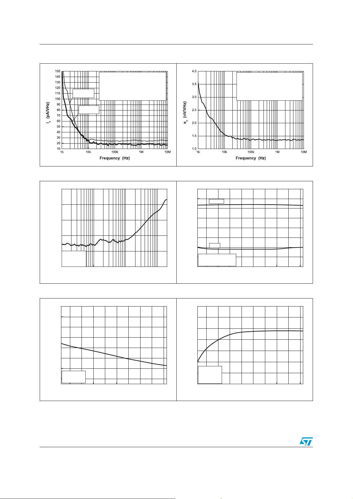
Electrical characteristics RHF330
Gain=37dB
Rg=10ohms
Rfb=750ohms
non-inverting input in short-circuit
Vcc=5V
-40 -20 0 20 40 60 80 100 120
-2.0
-1.5
-1.0
-0.5
0.0
0.5
1.0
1.5
2.0
Output: short-circuit
Vcc=5V
Iout (A)
Isource
Isink
Temperature (°C)
-40 -20 0 20 40 60 80 100 120
50
55
60
65
70
75
80
85
Gain=+1
Vcc=5V
Load=100
Ω
SVR (dB)
Temperature (°C)
Figure 13. Input current noise vs. frequency Figure 14. Input voltage noise vs. frequency
Gain=14.1dB
Rg=180ohms
Rfb=750ohms
Neg. Current
Noise
Pos. Current
Noise
Figure 15. Reverse isolation vs. frequency Figure 16. I
0
-20
-40
non-inverting input in short-circuit
Vcc=5V
vs. temperature
out
-60
Gain (dB)
-80
Small Signal
Vcc=5V
Ω
Load=100
-100
1M 10M 100M 1G
Figure 17. CMR vs. temperature Figure 18. SVR vs. temperature
60
58
56
54
52
CMR (dB)
50
48
Vcc=5V
46
8/22 Doc ID 15576 Rev 3
Ω
Load=100
-40 -20 0 20 40 60 80 100 120
Frequency (Hz)
Temperature (°C)
Page 9
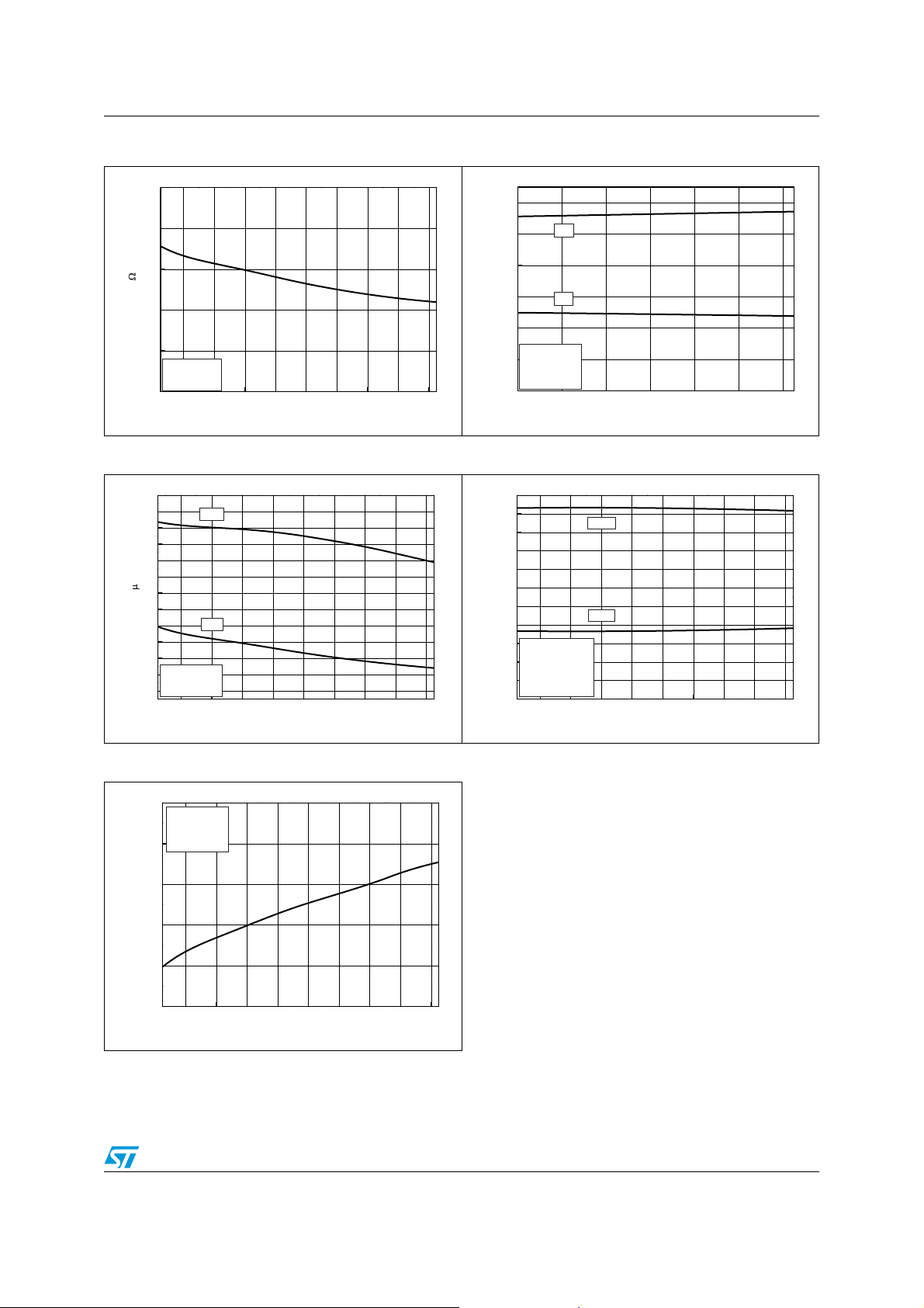
RHF330 Electrical characteristics
-40-200 20406080
-4
-3
-2
-1
0
1
2
Gain=+2
Vcc=5V
Load=100
Ω
VOL
VOH
V
OH & OL
(V)
Temperature (°C)
-40 -20 0 20 40 60 80 100 120
-35
-30
-25
-20
-15
-10
-5
0
5
10
15
20
Gain=+2
Vcc=5V
no Load
In+/In- to GND
Icc(+)
Icc(-)
Temperature ( C)
I
CC
(mA)
Figure 19. ROL vs. temperature Figure 20. VOH and VOL vs. temperature
180
160
140
(M )
OL
120
R
100
Open Loop
Vcc=5V
80
-40 -20 0 20 40 60 80 100 120
Figure 21. I
30
28
26
24
22
20
18
16
I bias ( A)
14
12
10
8
Vcc=5V
Load=100
6
-40 -20 0 20 40 60 80 100 120
bias
Ib(+)
Ib(−)
Temperature (°C)
vs. temperature Figure 22. ICC vs. temperature
Ω
Temperature (°C)
Figure 23. V
1000
800
600
(micro V)
IO
400
V
200
0
vs. temperature
io
Open Loop
Vcc=5V
Ω
Load=100
-40 -20 0 20 40 60 80 100 120
Temperature ( C)
Doc ID 15576 Rev 3 9/22
Page 10
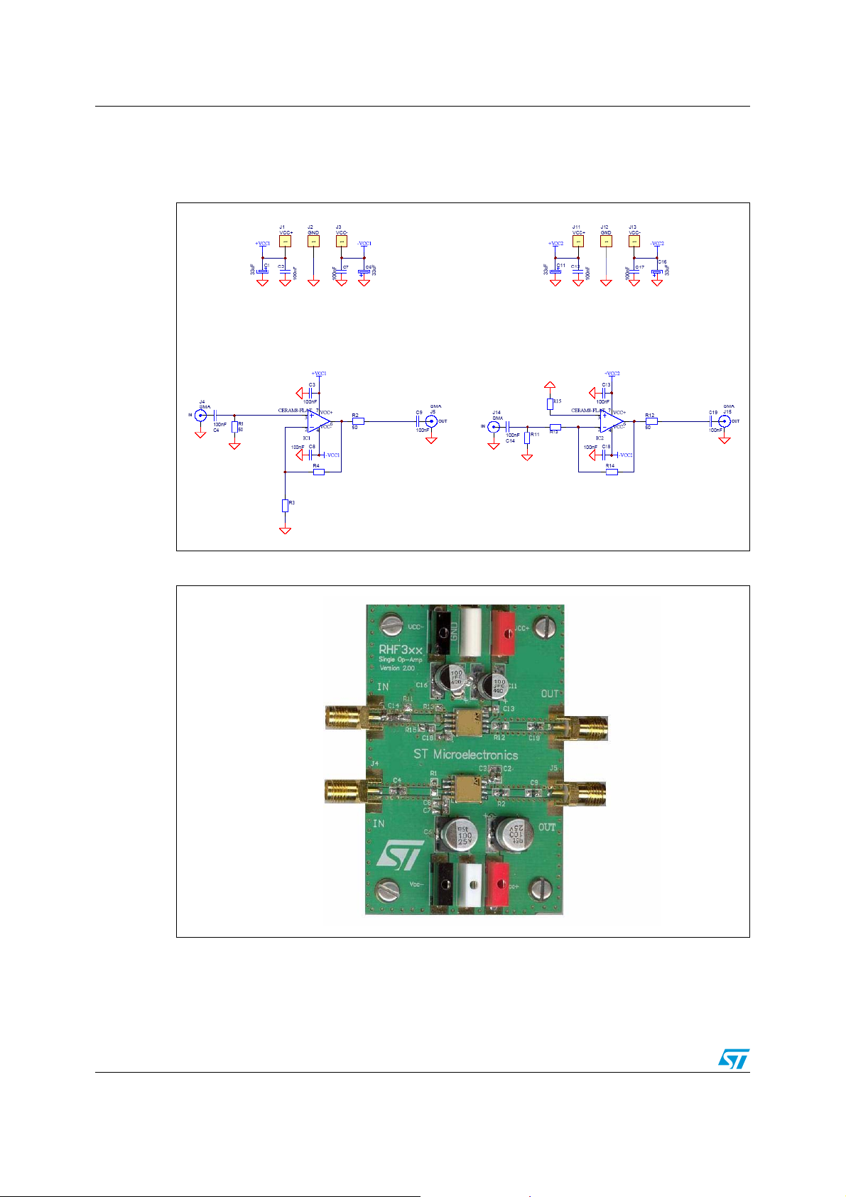
Demonstration board schematics RHF330
3 Demonstration board schematics
Figure 24. Electrical schematics (inverting and non-inverting gain configurations)
Figure 25. RHF3xx demonstration board
10/22 Doc ID 15576 Rev 3
Page 11
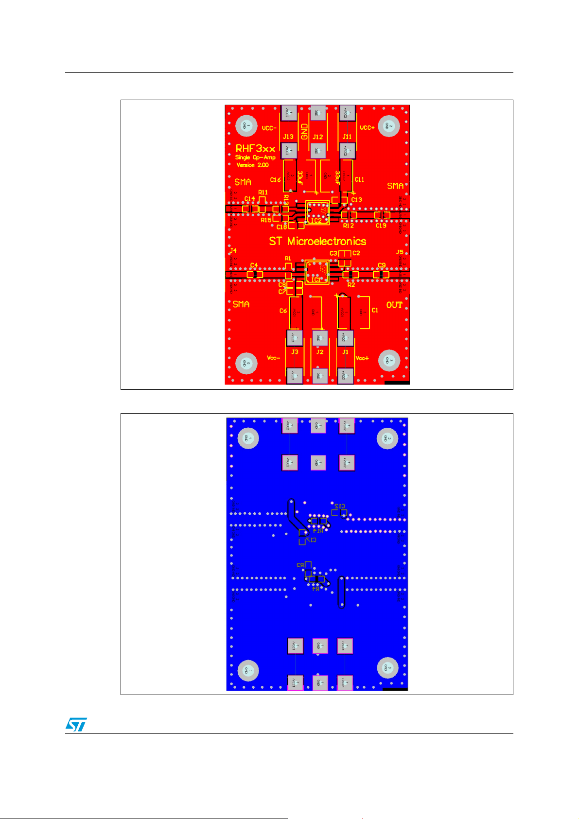
RHF330 Demonstration board schematics
Figure 26. Top view layout
Figure 27. Bottom view layout
Doc ID 15576 Rev 3 11/22
Page 12
Power supply considerations RHF330
4 Power supply considerations
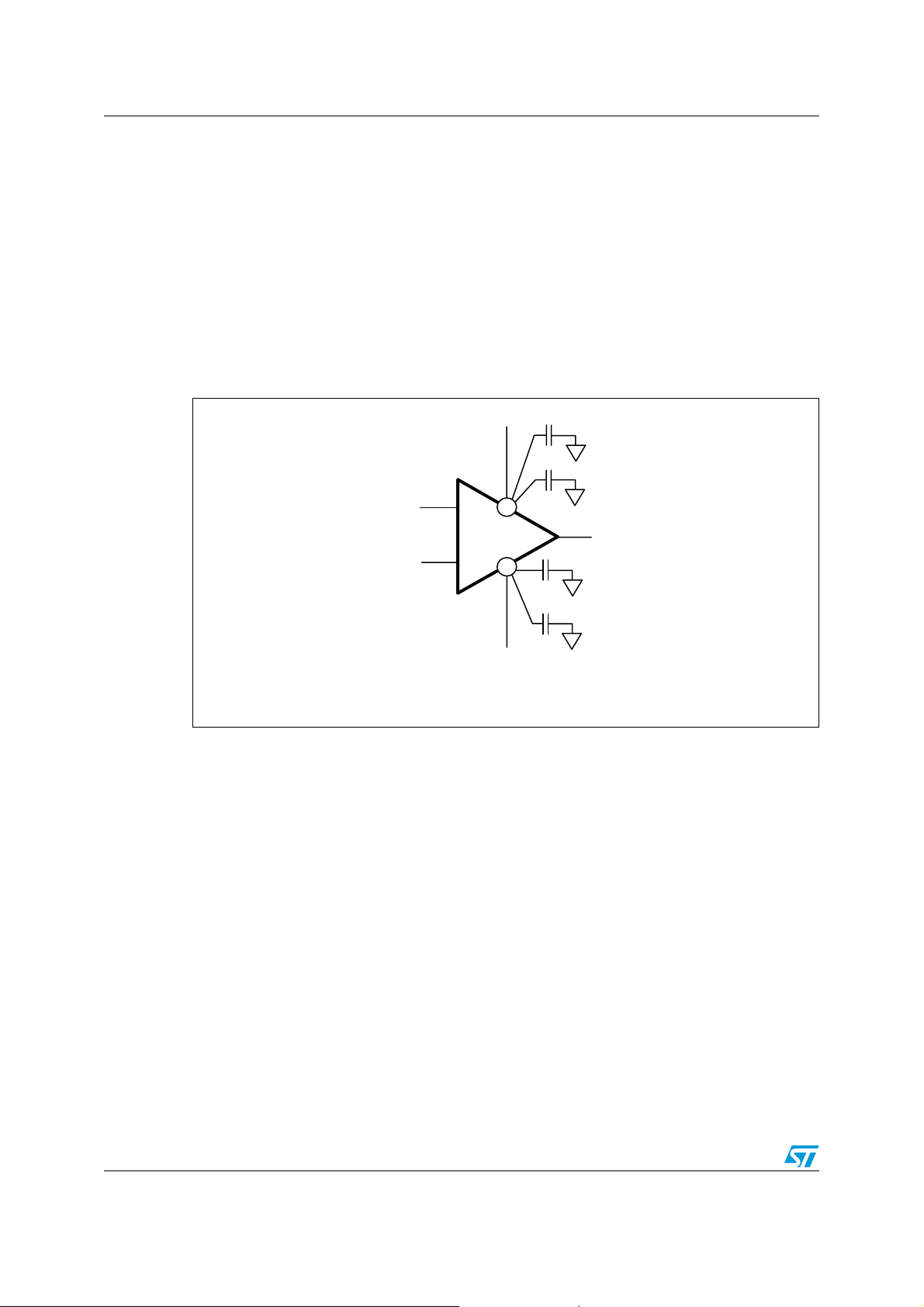
Correct power supply bypassing is very important for optimizing performance in highfrequency ranges. The bypass capacitors should be placed as close as possible to the IC
pins to improve high-frequency bypassing. A capacitor greater than 1 μF is necessary to
minimize the distortion. For better quality bypassing, a 10 nF capacitor can be added. It
should also be placed as close as possible to the IC pins. The bypass capacitors must be
incorporated for both the negative and the positive supply.
For example, on the RHF3xx single op-amp demonstration board, these capacitors are C6,
C7, C8, C9.
Figure 28. Circuit for power supply bypassing
+V
CC
10 µF
+
10 nF
+
4.1 Single power supply
In the event that a single supply system is used, biasing is necessary to obtain a positive
output dynamic range between 0 V and +V
and V
The amplifier must be biased with a mid-supply (nominally +V
DC component of the signal at this value. Several options are possible to provide this bias
supply, such as a virtual ground using an operational amplifier or a two-resistance divider
(which is the cheapest solution). A high resistance value is required to limit the current
consumption. On the other hand, the current must be high enough to bias the non-inverting
input of the amplifier. If we consider this bias current (55 μA maximum) as 1% of the current
through the resistance divider, to keep a stable mid-supply, two resistances of 470 Ω can be
used.
The input provides a high-pass filter with a break frequency below 10 Hz which is necessary
to remove the original 0 V DC component of the input signal, and to set it at +V
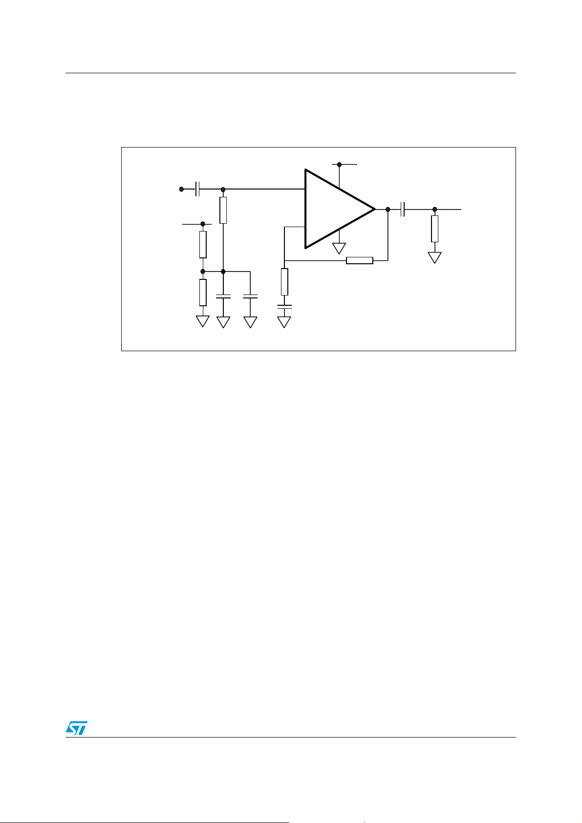
Figure 29 on page 13 illustrates a 5 V single power supply configuration for the RHF3xx
single op-amp demonstration board.
, the amplifier provides an output swing from +0.9 V to +4.1 V on a 100 Ω load.
OL
-
-V
supply rails. Considering the values of VOH
CC
10 nF
10 µF
+
CC
AM00835
/2), in order to maintain the
CC
CC
/2.
12/22 Doc ID 15576 Rev 3
Page 13
RHF330 Power supply considerations
A capacitor CG is added in the gain network to ensure a unity gain at low frequencies to
keep the right DC component at the output. C
contributes to a high-pass filter with Rfb//RG
G
and its value is calculated with regard to the cut-off frequency of this low-pass filter.
Figure 29. Circuit for +5 V single supply
+5 V
10 µF
IN
+5 V
R1
470 Ω
R2
470 Ω
R
1 kΩ
+ 1 µF
in
10 nF
+
+
_
R
fb
R
G
C
G
100 µ F
OUT
100 Ω
AM00836
Doc ID 15576 Rev 3 13/22
Page 14
Noise measurements RHF330
5 Noise measurements
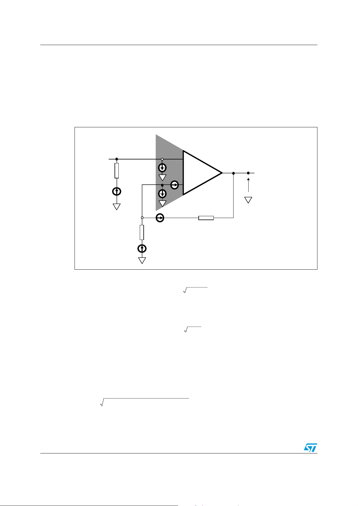
The noise model is shown in Figure 30.
● eN: input voltage noise of the amplifier
● iNn: negative input current noise of the amplifier
● iNp: positive input current noise of the amplifier
Figure 30. Noise model
+
R3
N3
iN
iN
+
_
eN
-
Output
HP3577
Input noise:
8 nV/√Hz
R1
N2
R2
N1
AM00837
The thermal noise of a resistance R is:
4kTRΔF
where ΔF is the specified bandwidth.
On a 1 Hz bandwidth the thermal noise is reduced to:
4kTR
where k is the Boltzmann's constant, equal to 1,374.E(-23)J/°K. T is the temperature (°K).
The output noise eNo is calculated using the superposition theorem. However, eNo is not
the simple sum of all noise sources but rather the square root of the sum of the square of
each noise source, as shown in Equation 1.
Equation 1
eNo V12V22V32V42V52V6
+++++=
2
14/22 Doc ID 15576 Rev 3
Page 15

RHF330 Noise measurements
Equation 2
2
eNo2eN2g2iNn2R22iNp
+×+× R3
2
× g2×
2
R2
------- -
4kTR1 4kTR2 1
R1
The input noise of the instrumentation must be extracted from the measured noise value.
The real output noise value of the driver is:
Equation 3
2
instrumentation()
eNo Measured()
–=
The input noise is called equivalent input noise because it is not directly measured but is
evaluated from the measurement of the output divided by the closed loop gain (eNo/g).
After simplification of the fourth and the fifth term of Equation 2 we obtain:
Equation 4
2
eNo2eN2g2iNn2R22iNp
+×+× R3
2
× g2× g4kTR21
5.1 Measurement of the input voltage noise eN
If we assume a short-circuit on the non-inverting input (R3=0), from Equation 4 we can
derive:
2
R2
------- -+
4kTR3×++×+=
R1
2
2
R2
------- -+
4kTR3×+×+=
R1
Equation 5
eNo eN
2g2
iNn2R22g4kTR2×+×+×=
To easily extract the value of eN, the resistance R2 is as low as possible. On the other hand,
the gain must be large enough.
R3=0, gain: g=100
5.2 Measurement of the negative input current noise iNn
To measure the negative input current noise iNn, we set R3=0 and use Equation 5. This
time, the gain must be lower to decrease the thermal noise contribution.
R3=0, gain: g=10
5.3 Measurement of the positive input current noise iNp
To extract iNp from Equation 3, a resistance R3 is connected to the non-inverting input. The
value of R3 must be chosen so that its thermal noise contribution is as low as possible
against the iNp contribution.
R3=100 W, gain: g=10
Doc ID 15576 Rev 3 15/22
Page 16

Intermodulation distortion product RHF330
6 Intermodulation distortion product
The non-ideal output of the amplifier can be described by the following series of equations.
2
Where the input is V
V
=Asinωt, C0 is the DC component, C1(Vin) is the fundamental and C
in
C0C1VinC2V
out
++ +=
the amplitude of the harmonics of the output signal V
in
out
… C+nV
n
in
is
n
.
A one-frequency (one-tone) input signal contributes to harmonic distortion. A two-tone input
signal contributes to harmonic distortion and to the intermodulation product.
The study of the intermodulation and distortion for a two-tone input signal is the first step in
characterizing the driving capability of multi-tone input signals.
In this case:
VinA ω1tsin A ω2tsin+=
Then:
C0C1A ω1tsin A ω2tsin+()C2A ω1tsin A ω2tsin+()
V
out
++ +=
2
… CnA ω1tsin A ω2tsin+()
n
From this expression, we can extract the distortion terms and the intermodulation terms
from a single sine wave.
● Second order intermodulation terms IM2 by the frequencies (ω
amplitude of C2A
● Third order intermodulation terms IM3 by the frequencies (2ω
and (ω
+2ω2) with an amplitude of (3/4)C3A3.
1
2
.
) and (ω1+ω2) with an
1-ω2
), (2ω1+ω2), (−ω1+2ω2)
1-ω2
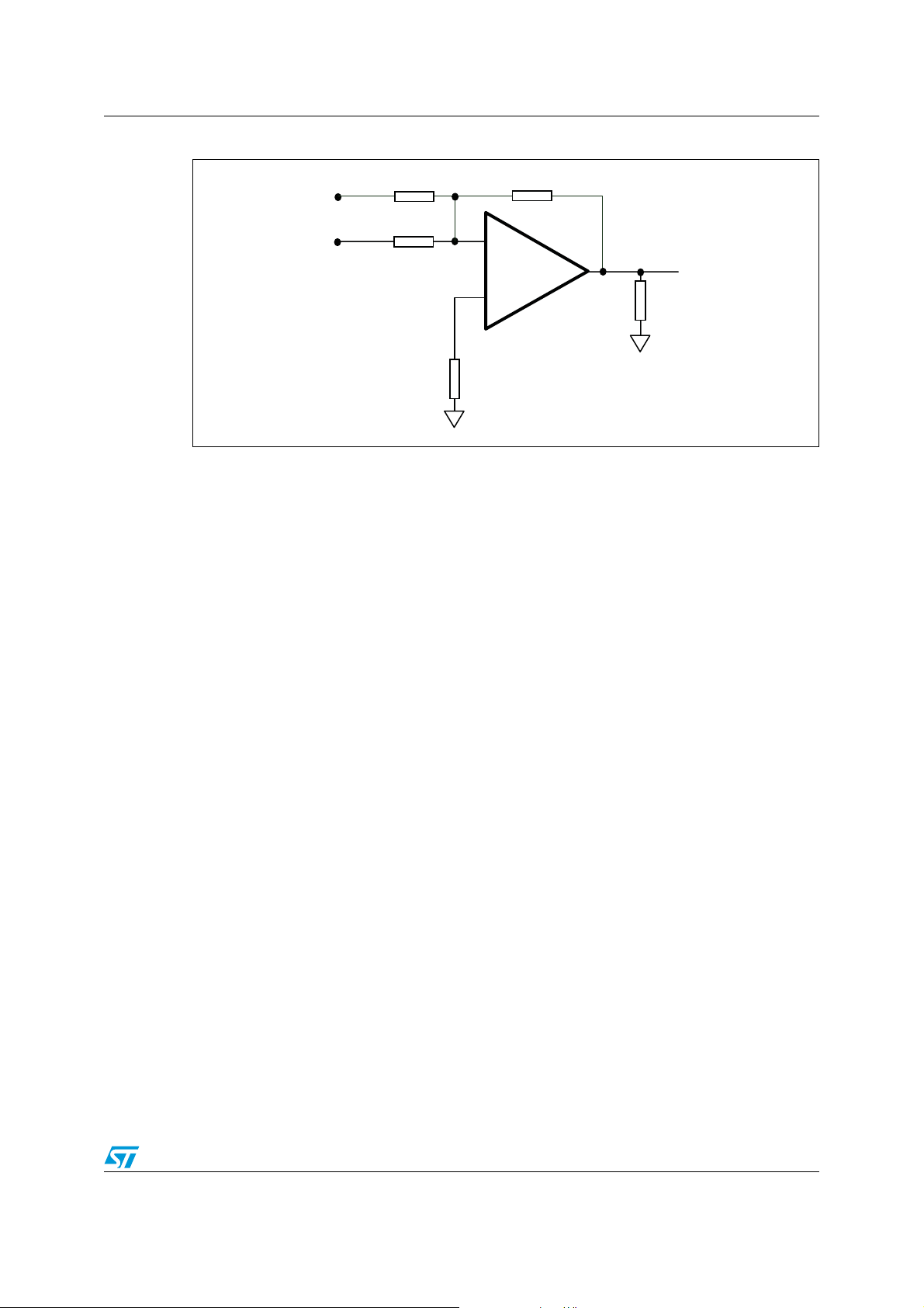
The intermodulation product of the driver is measured by using the driver as a mixer in a
summing amplifier configuration (Figure 31 on page 17). In this way, the non-linearity
problem of an external mixing device is avoided.
16/22 Doc ID 15576 Rev 3
Page 17
RHF330 Intermodulation distortion product
Figure 31. Inverting summing amplifier
V
in1
V
in2
R
1
R
2
R
fb
_
V
out
+
100 Ω
R
AM00838
Doc ID 15576 Rev 3 17/22
Page 18
Bias of an inverting amplifier RHF330
7 Bias of an inverting amplifier
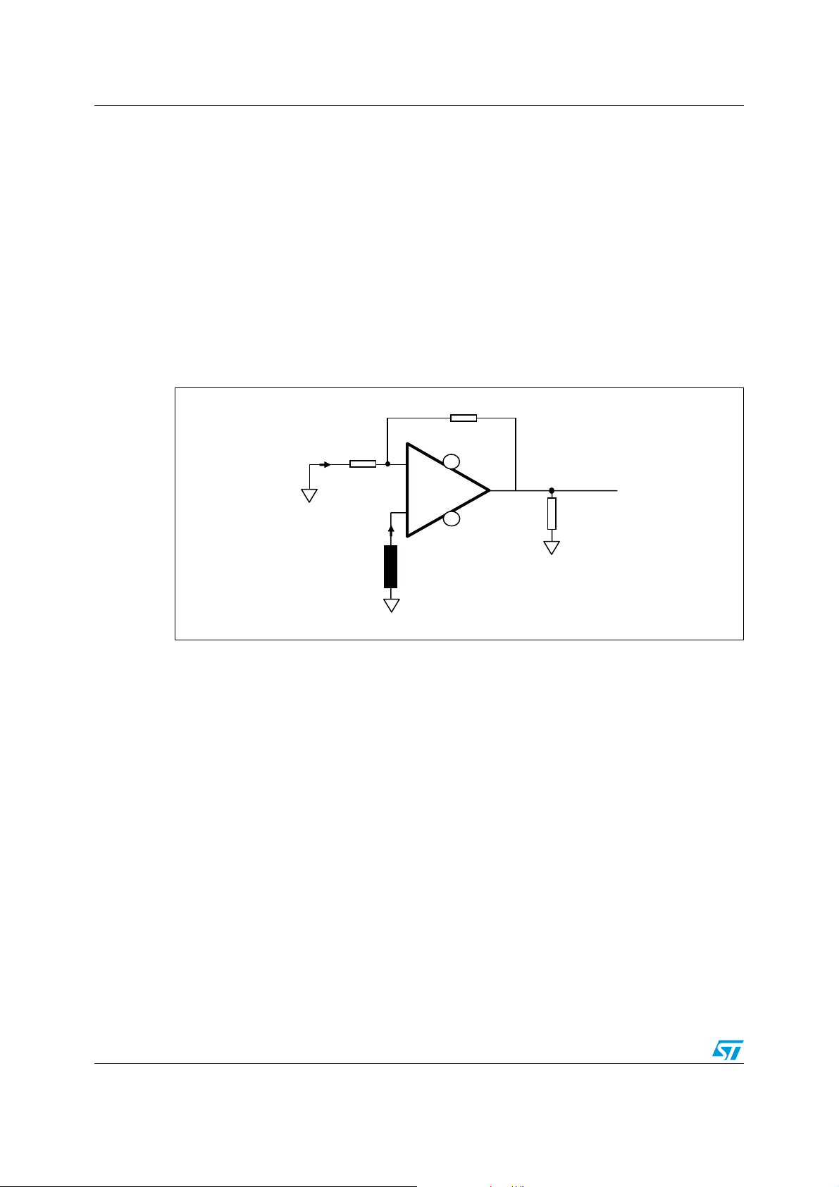
A resistance is necessary to achieve good input biasing, such as resistance R shown in
Figure 32.
The value of this resistance is calculated from the negative and positive input bias current.
The aim is to compensate for the offset bias current, which can affect the input offset voltage
and the output DC component. Assuming I
resistance R is:
Figure 32. Compensation of the input bias current
R
-
I
ib
in
, I
, Rin, Rfb and a zero volt output, the
ib-
ib+
R
×
inRfb
R
------------------------=
R
R+
in
fb
R
fb
_
VCC+
Output
+
+
I
ib
-
V
CC
Load
R
AM00839
18/22 Doc ID 15576 Rev 3
Page 19
RHF330 Active filtering
8 Active filtering
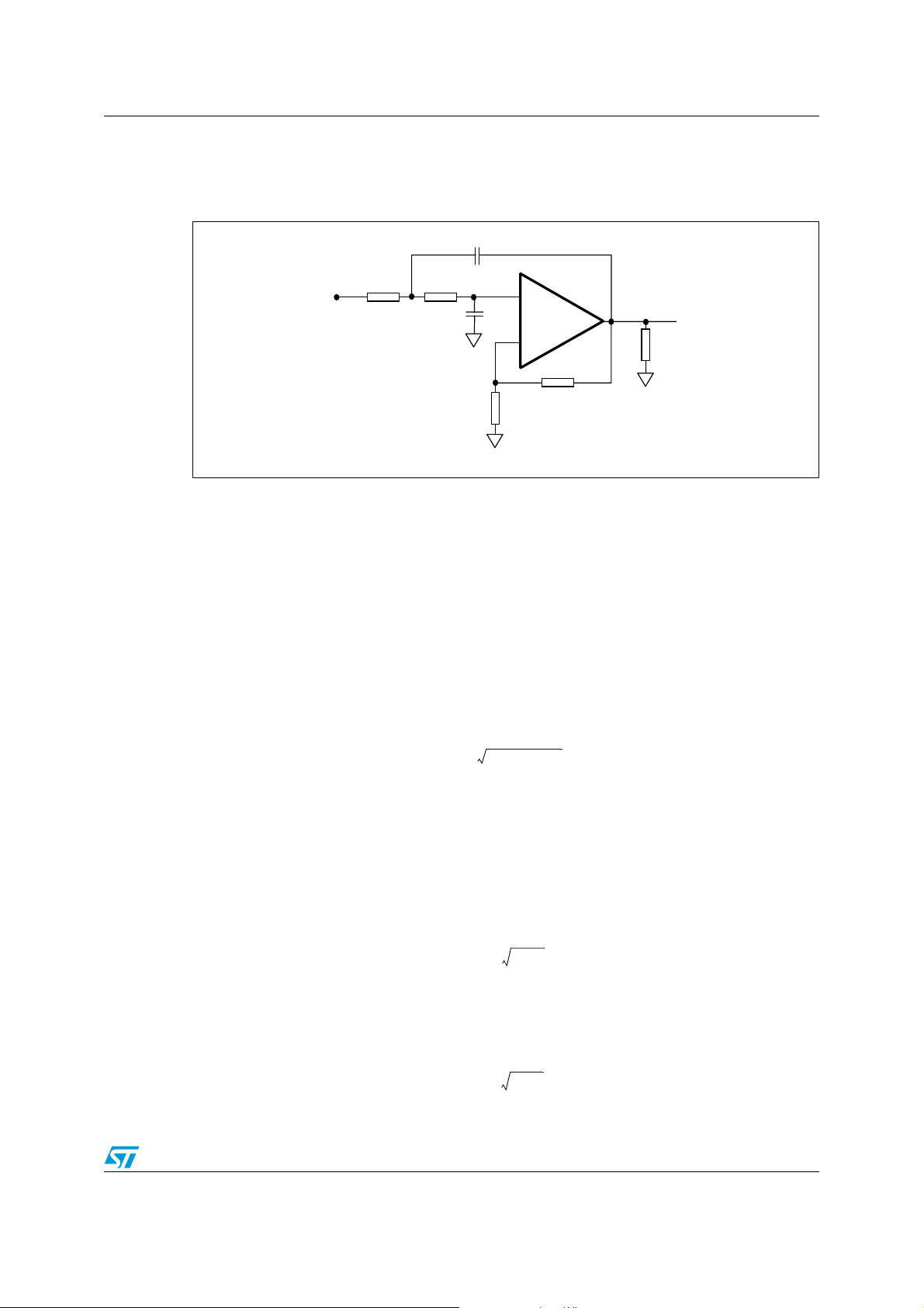
Figure 33. Low-pass active filtering, Sallen-Key
C1
1
R
IN
2
R
C2
+
OUT
_
R
fb
From the resistors R
R
G
and RG we can directly calculate the gain of the filter in a classic non-
fb
inverting amplification configuration.
R
AVg1
fb
--------+==
R
g
We assume the following expression is the response of the system.
Vout
---------------- -
Vin
jω
jω
T
jω
---------------------------------------- -==
12ζ
g
jω
-----
ω
2
jω()
----------- -++
2
c
ω
c
The cut-off frequency is not gain-dependent and so becomes:
100 Ω
AM00840
ω
c
1
------------------------------------ -=
R1R2C1C2
The damping factor is calculated by the following expression.
1
-- -
ζ
ωcC1R1C1R2C2R1C1R1g–++()=
2
The higher the gain, the more sensitive the damping factor is. When the gain is higher than
1, it is preferable to use very stable resistor and capacitor values. In the case of R1=R2=R:
R
fb
–
2C1
2C1C
--------
R
2
g
2C
ζ
-------------------------------- -=
Due to a limited selection of capacitor values in comparison with the resistors, we can set
C1=C2=C, so that:
2R
ζ
-------------------------------- -=
Doc ID 15576 Rev 3 19/22
–
2R1
2R
1R2
R
--------
R
fb
g
Page 20
Package information RHF330
9 Package information
In order to meet environmental requirements, ST offers these devices in different grades of
ECOPACK
specifications, grade definitions and product status are available at: www.st.com.
ECOPACK
®
packages, depending on their level of environmental compliance. ECOPACK®
®
is an ST trademark.
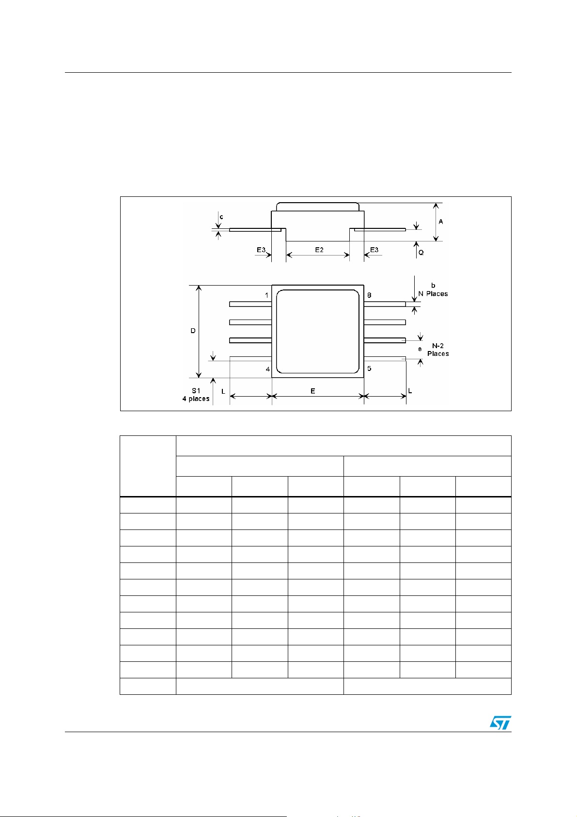
Figure 34. Ceramic Flat-8 package mechanical drawing
Table 6. Ceramic Flat-8 package mechanical data
Dimensions
Ref.
Millimeters Inches
Min. Typ. Max. Min. Typ. Max.
A 2.24 2.44 2.64 0.088 0.096 0.104
b 0.38 0.43 0.48 0.015 0.017 0.019
c 0.10 0.13 0.16 0.004 0.005 0.006
D 6.35 6.48 6.61 0.250 0.255 0.260
E 6.35 6.48 6.61 0.250 0.255 0.260
E2 4.32 4.45 4.58 0.170 0.175 0.180
E3 0.88 1.01 1.14 0.035 0.040 0.045
e 1.27 0.050
L 3.00 0.118
Q 0.66 0.79 0.92 0.026 0.031 0.092
S1 0.92 1.12 1.32 0.036 0.044 0.052
N08 08
20/22 Doc ID 15576 Rev 3
Page 21
RHF330 Revision history
10 Revision history
Table 7. Document revision history
Date Revision Changes
20-May-2009 1 Initial release.
04-May-2010 2
27-May-2010 3
Modified temperature limits in Ta b le 4 .
Changed order codes in Ta b le 7 .
Added Mass in Features on cover page.
Added full ordering information in Ta bl e 1 .
Doc ID 15576 Rev 3 21/22
Page 22

RHF330
Please Read Carefully:
Information in this document is provided solely in connection with ST products. STMicroelectronics NV and its subsidiaries (“ST”) reserve the
right to make changes, corrections, modifications or improvements, to this document, and the products and services described herein at any
time, without notice.
All ST products are sold pursuant to ST’s terms and conditions of sale.
Purchasers are solely responsible for the choice, selection and use of the ST products and services described herein, and ST assumes no
liability whatsoever relating to the choice, selection or use of the ST products and services described herein.
No license, express or implied, by estoppel or otherwise, to any intellectual property rights is granted under this document. If any part of this
document refers to any third party products or services it shall not be deemed a license grant by ST for the use of such third party products
or services, or any intellectual property contained therein or considered as a warranty covering the use in any manner whatsoever of such
third party products or services or any intellectual property contained therein.
UNLESS OTHERWISE SET FORTH IN ST’S TERMS AND CONDITIONS OF SALE ST DISCLAIMS ANY EXPRESS OR IMPLIED
WARRANTY WITH RESPECT TO THE USE AND/OR SALE OF ST PRODUCTS INCLUDING WITHOUT LIMITATION IMPLIED
WARRANTIES OF MERCHANTABILITY, FITNESS FOR A PARTICULAR PURPOSE (AND THEIR EQUIVALENTS UNDER THE LAWS
OF ANY JURISDICTION), OR INFRINGEMENT OF ANY PATENT, COPYRIGHT OR OTHER INTELLECTUAL PROPERTY RIGHT.
UNLESS EXPRESSLY APPROVED IN WRITING BY AN AUTHORIZED ST REPRESENTATIVE, ST PRODUCTS ARE NOT
RECOMMENDED, AUTHORIZED OR WARRANTED FOR USE IN MILITARY, AIR CRAFT, SPACE, LIFE SAVING, OR LIFE SUSTAINING
APPLICATIONS, NOR IN PRODUCTS OR SYSTEMS WHERE FAILURE OR MALFUNCTION MAY RESULT IN PERSONAL INJURY,
DEATH, OR SEVERE PROPERTY OR ENVIRONMENTAL DAMAGE. ST PRODUCTS WHICH ARE NOT SPECIFIED AS "AUTOMOTIVE
GRADE" MAY ONLY BE USED IN AUTOMOTIVE APPLICATIONS AT USER’S OWN RISK.
Resale of ST products with provisions different from the statements and/or technical features set forth in this document shall immediately void
any warranty granted by ST for the ST product or service described herein and shall not create or extend in any manner whatsoever, any
liability of ST.
ST and the ST logo are trademarks or registered trademarks of ST in various countries.
Information in this document supersedes and replaces all information previously supplied.
The ST logo is a registered trademark of STMicroelectronics. All other names are the property of their respective owners.
© 2010 STMicroelectronics - All rights reserved
STMicroelectronics group of companies
Australia - Belgium - Brazil - Canada - China - Czech Republic - Finland - France - Germany - Hong Kong - India - Israel - Italy - Japan -
Malaysia - Malta - Morocco - Philippines - Singapore - Spain - Sweden - Switzerland - United Kingdom - United States of America
www.st.com
22/22 Doc ID 15576 Rev 3
 Loading...