

Page 1
RF3V49092, RF3S49092SM
Data Sheet November 1999 File Number 4600.1
20A/10A, 12V, 0.060/0.140 Ohm, Logic
Level, Complementary Power MOSFET
These complementary power MOSFETs are manufactured
using an advanced MegaFET process. This process, which
uses feature sizes approaching those of LSI integrated
circuits, gives optimum utilization of silicon, resulting in
outstanding performance. It is designed for use in
applications such as switching regulators, switching
converters, motor drivers, relay drivers, and low voltage bus
switches. This product achieves full rated conduction at a
gate bias in the 3V to 5V range, thereby facilitating true
on-off power control directly from logic level (5V) integrated
circuits.
Formerly developmental type TA49092.
Ordering Information
PART NUMBER PACKAGE BRAND
RF3V49092 TS-001AA F3V49092
RF3S49092SM MO-169AB F3S49092
NOTE: Whenordering, use the entire part number.Forordering the
MO-169ABintape and reel, add thesuffix9A to the part number,i.e.,
RF3S49092SM9A.
Features
• 20A, 12V (N-Channel)
10A, 12V (P-Channel)
•r
r
• Temperature Compensating PSPICE
= 0.060Ω (N-Channel)
DS(ON)
= 0.140Ω (P-Channel)
DS(ON)
®
Model
• On-Resistance vs Gate Drive Voltage Curves
• Peak Current vs Pulse Width Curve
• UIS Rating Curve
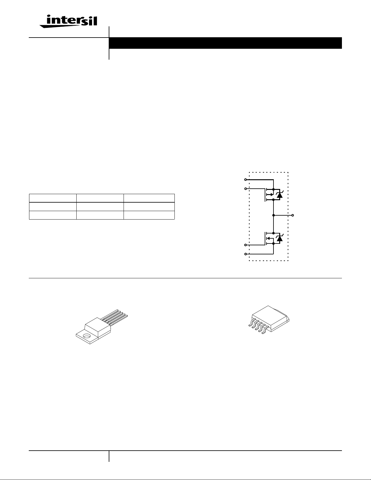
Symbol
S2
G2
D1
G1
S1
Packaging
JEDEC TS-001AA (ALTERNATE) JEDEC MO-169AB
S1
G1
D
S2
G2
G2
S2
D
G1
S1
4-30
CAUTION: These devices are sensitive to electrostatic discharge; follow proper ESD Handling Procedures.
PSPICE® is a registered trademark of MicroSim Corporation.
1-888-INTERSIL or 321-727-9207
| Copyright © Intersil Corporation 1999
Page 2
RF3V49092, RF3S49092SM
Absolute Maximum Ratings T
= 25oC Unless Otherwise Specified
C
N-CHANNEL P-CHANNEL UNITS
Drain to Source Voltage (Note 1). . . . . . . . . . . . . . . . . .V
Drain to Gate Voltage (RGS= 20kΩ, Note 1). . . . . . . . .V
Gate to Source Voltage . . . . . . . . . . . . . . . . . . . . . . . . . .V
DSS
DGR
GS
12 -12 V
12 -12 V
±10 ±10 V
Drain Current
Continuous. . . . . . . . . . . . . . . . . . . . . . . . . . . . . . . . . . . .I
Pulsed (Figures 5, 26) . . . . . . . . . . . . . . . . . . . . . . . . . I
Pulsed Avalanche Rating (Figures 6, 27). . . . . . . . . . . . .E
DM
AS
D
Refer to Peak Current Curve
20
10
Refer to Peak Current Curve
Refer to UIS Curve Refer to UIS Curve
A
Power Dissipation
TC = 25oC . . . . . . . . . . . . . . . . . . . . . . . . . . . . . . . . . . . P
D
Derate Above 25oC . . . . . . . . . . . . . . . . . . . . . . . . . . . . . .
Operating and Storage Temperature . . . . . . . . . . . . TJ, T
STG
Maximum Temperature for Soldering
Leads at 0.063in (1.6mm) from Case for 10s. . . . . . . . . T
Package Body for 10s, See Techbrief 334 . . . . . . . . . .T
CAUTION: Stresses above those listed in “Absolute Maximum Ratings” may cause permanent damage to the device. This is a stress only rating and operation of the
device at these or any other conditions above those indicated in the operational sections of this specification is not implied.
L
pkg
50
0.33
50
0.33
-55 to 175 -55 to 175
300
260
300
260
W
W/oC
o
C
o
C
o
C
NOTE:
1. TJ = 25oC to 150oC.
Electrical Specifications (N-Channel) T
= 25oC, Unless Otherwise Specified
C
PARAMETER SYMBOL TEST CONDITIONS MIN TYP MAX UNITS
Drain to Source Breakdown Voltage BV
Gate Threshold Voltage V
GS(TH)VGS
Zero Gate Voltage Drain Current I
Gate to Source Leakage Current I
Drain to Source On Resistance r
DS(ON)ID
Turn-On Time t
Turn-On Delay Time t
d(ON)
Rise Time t
Turn-Off Delay Time t
d(OFF)
Fall Time t
Turn-Off Time t
Total Gate Charge Q
g(TOT)VGS
Gate Charge at 5V Q
Threshold Gate Charge Q
Input Capacitance C
Output Capacitance C
Reverse Transfer Capacitance C
Thermal Resistance Junction to Case R
Thermal Resistance Junction to Ambient R
DSSID
DSS
GSS
ON
r
f
OFF
g(5)
g(TH)
ISS
OSS
RSS
JC
θ
JA
θ
= 250µA, VGS = 0V, (Figure 13) 12 - - V
= VDS, ID = 250µA, (Figure 12) 1 - - V
VDS = 12V,
VGS = 0V
TC = 25oC--1µA
TC = 150oC--50µA
VGS = ±10V - - ±100 nA
= 20A, VGS = 5V, (Figure 9, 11) - - 0.060 Ω
VDD = 6V, ID≈ 20A, RL = 0.24Ω,
VGS= 5V, RGS = 25Ω
(Figure 10)
- - 100 ns
-18-ns
-60-ns
-50-ns
-60-ns
- - 140 ns
= 0V to 10V VDD = 9.6V,
VGS = 0V to 5V - 12 15 nC
VGS = 0V to 1V - 0.9 1.2 nC
ID = 20A,
RL = 0.42Ω
(Figure 15)
VDS = 10V, VGS = 0V, f = 1MHz
(Figure 14)
-2025nC
- 750 - pF
- 700 - pF
- 275 - pF
- - 3.00
TS-001AA, and MO-169AB - - 62
o
o
C/W
C/W
N-Channel Source to Drain Diode Specifications
PARAMETER SYMBOL TEST CONDITIONS MIN TYP MAX UNITS
Source to Drain Voltage V
Reverse Recovery Time t
4-31
SD
ISD = 20A - - 1.5 V
ISD = 20A, dISD/dt = 100A/µs - - 100 ns
rr
Page 3
RF3V49092, RF3S49092SM
Electrical Specifications (P-Channel) T
PARAMETER SYMBOL TEST CONDITIONS MIN TYP MAX UNITS
Drain to Source Breakdown Voltage BV
Gate Threshold Voltage V
Zero Gate Voltage Drain Current I
Gate to Source Leakage Current I
Drain to Source On Resistance r
Turn-On Time t
Turn-On Delay Time t
Rise Time t
Turn-Off Delay Time t
Fall Time t
Turn-Off Time t
Total Gate Charge Q
Gate Charge at -5V Q
Threshold Gate Charge Q
Input Capacitance C
Output Capacitance C
Reverse Transfer Capacitance C
Thermal Resistance Junction to Case R
Thermal Resistance Junction to Ambient R
DS(ON)ID
d(OFF)
= 25oC, Unless Otherwise Specified
C
DSSID
GS(TH)VGS
DSS
= 250µA, VGS = 0V, (Figure 34) -12 - - V
= VDS, ID = 250µA, (Figure 33) -1 - - V
VDS = -12V,
VGS = 0V
GSS
VGS = ±10V - - ±100 nA
= 10A, VGS = -5V, (Figures 30, 32) - - 0.140 Ω
ON
VDD = -6V, ID≈ 10A, RL = 0.62Ω,
VGS= -5V, RGS = 25Ω
d(ON)
OFF
g(TOT)VGS
g(-5)
g(TH)
ISS
(Figure 31)
r
f
= 0V to -10V VDD = -9.6V,
VGS = 0V to -5V - 10 14 nC
VGS = 0V to -1V - 0.8 1.1 nC
VDS = -10V, VGS = 0V, f = 1MHz
(Figure 35)
OSS
RSS
θJC
TS-001AA, and MO-169AB - - 62
JA
θ
TC = 25oC---1µA
TC = 150oC - - -50 µA
- - 115 ns
-25-ns
-65-ns
-40-ns
-45-ns
- - 110 ns
-1924nC
ID = 10A,
RL = 1.0Ω
(Figure 36)
- 775 - pF
- 550 - pF
- 150 - pF
- - 3.00
o
o
C/W
C/W
P-Channel Source to Drain Diode Specifications
PARAMETER SYMBOL TEST CONDITIONS MIN TYP MAX UNITS
Source to Drain Voltage V
Reverse Recovery Time t
SD
ISD = -10A - - -1.5 V
ISD = -10A, dISD/dt = -100A/µs - - 100 ns
rr
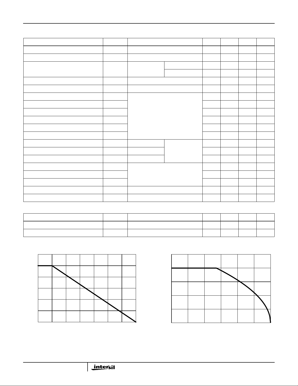
Typical Performance Curves (N-Channel)
1.2
1.0
0.8
0.6
0.4
0.2
POWER DISSIPATION MULTIPLIER
0
0 25 50 75 100 150
TC, CASE TEMPERATURE (oC)
FIGURE 1. NORMALIZED POWERDISSIPATION vs CASE
TEMPERATURE
125
175
25
20
15
10
, DRAIN CURRENT (A)
D
I
5
0
25 50 75 100 125 175
TC, CASE TEMPERATURE (oC)
150
FIGURE 2. MAXIMUM CONTINUOUS DRAIN CURRENT vs
CASE TEMPERATURE
4-32
Page 4
RF3V49092, RF3S49092SM
Typical Performance Curves (N-Channel) (Continued)
DUTY CYCLE - DESCENDING ORDER
0.5
1
0.2
0.1
0.05
0.02
0.01
0.1
, NORMALIZED
JC
θ
Z
THERMAL IMPEDANCE
SINGLE PULSE
0.01
-5
10
-4
10
FIGURE 3. NORMALIZED MAXIMUM TRANSIENT THERMAL IMPEDANCE
-3
10
10
t, RECTANGULAR PULSE DURATION (s)
P
DM
t
1
t
NOTES:
DUTY FACTOR: D = t
PEAK TJ = PDM x Z
-2
-1
10
0
10
2
1/t2
x R
JC
θ
+ T
JC
C
θ
1
10
100
TJ = MAX RATED, TC = 25oC
1000
TC = 25oC
FOR TEMPERATURES
ABOVE 25
o
C DERATE PEAK
CURRENT AS FOLLOWS:
175 - T
25
-1
10
10
, DRAIN CURRENT (A)
OPERATION IN THIS
D
I
AREA MAY BE
LIMITED BY r
1
1
VDS, DRAIN TO SOURCE VOLTAGE (V)
DS(ON)
5ms
10ms
100ms
1s
DC
10 50
100
VGS = 5V
TRANSCONDUCTANCE
, PEAK CURRENT CAPABILITY (A)
MAY LIMIT CURRENT
DM
I
IN THIS REGION
10
-5
10
10
I = I
-4
-3
10
-2
10
t, PULSE WIDTH (s)
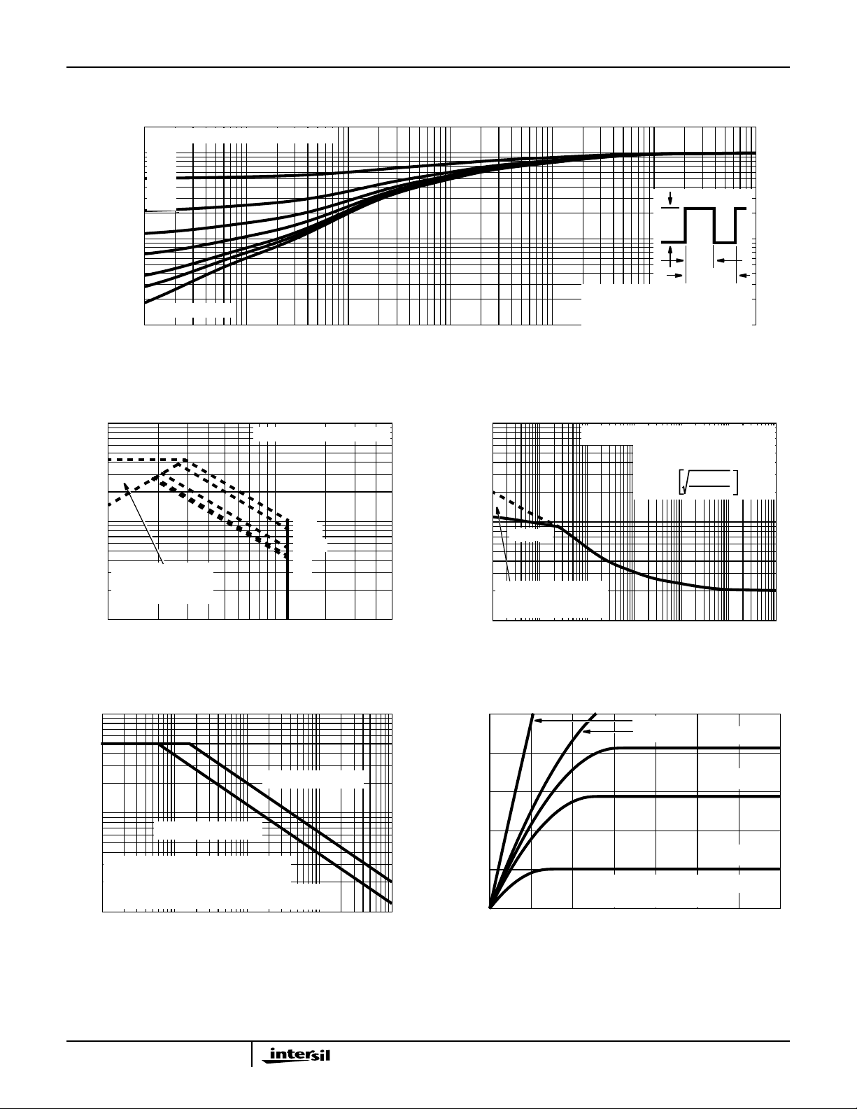
FIGURE 4. FORWARD BIAS SAFE OPERATING AREA FIGURE 5. PEAK CURRENT CAPABILITY
100
10
STARTING TJ = 150oC
If R = 0
, AVALANCHE CURRENT (A)
tAV = (L)(IAS)/(1.3*RATED BV
AS
I
If R ≠ 0
t
= (L/R)ln[(IAS*R)/(1.3*RATED BV
AV
1
0.01
0.1
tAV, TIME IN AVALANCHE (ms)
STARTING TJ = 25oC
- VDD)
DSS
- VDD) +1]
DSS
1 10 100
50
V
= 10V
GS
VGS = 5V
40
30
20
, DRAIN CURRENT (A)
D
I
10
PULSE DURATION = 80µs, TC = 25oC
0
012345
VDS, DRAIN TO SOURCE VOLTAGE (V)
DUTY CYCLE = 0.5% MAX
C
150
0
10
VGS = 4.5V
VGS = 4V
VGS = 3V
67
1
10
NOTE: Refer to Intersil Application Notes AN9321 and AN9322.
FIGURE 6. UNCLAMPED INDUCTIVE SWITCHING CAPABILITY
4-33
FIGURE 7. SATURATION CHARACTERISTICS
Page 5

RF3V49092, RF3S49092SM
Typical Performance Curves (N-Channel) (Continued)
50
40
30
20
, DRAIN CURRENT (A)
D
I
10
0
0 23451
VGS, GATE TO SOURCE VOLTAGE (V)
25oC
-55oC
PULSE DURATION = 80µs
DUTY CYCLE = 0.5% MAX
VDD= 6V
175oC
67
200
ID = 5A
150
ID = 10A
100
, DRAIN TO SOURCE
ON RESISTANCE (mΩ)
50
DS(ON)
r
PULSE DURATION = 80µs
DUTY CYCLE = 0.5% MAX
0
046810
2
V
GS
ID = 20A
, GATE TO SOURCE VOLTAGE (V)
FIGURE 8. TRANSFER CHARACTERISTICS FIGURE 9. DRAIN TO SOURCE ON RESISTANCEvs GATE
VOLTAGE AND DRAIN CURRENT
140
VDD = 6V, ID = 20A, RL= 0.24Ω
120
100
80
t
t
D(OFF)
r
1.6
PULSE DURATION = 80µs, VGS = 5V, ID = 20A
DUTY CYCLE = 0.5% MAX
1.4
1.2
t
t
D(ON)
f
1.0
ON RESISTANCE
0.8
NORMALIZED DRAIN TO SOURCE
0.6
-80 -40 0 40 80 120 160
TJ, JUNCTION TEMPERATURE (oC)
60
40
SWITCHING TIME (ns)
20
0
10
RGS, GATE TO SOURCE RESISTANCE (Ω)
20 30 40 500
FIGURE 10. SWITCHING TIME vs GATE RESISTANCE FIGURE11. NORMALIZED DRAIN TO SOURCE ON
RESISTANCE vs JUNCTION TEMPERATURE
1.2
1.0
0.8
NORMALIZED GATE
THRESHOLD VOLTAGE
0.6
-80 -40 0 40 80 120 160
TJ, JUNCTION TEMPERATURE (oC)
VGS = VDS, ID = 250µA
200
1.2
ID = 250µA
1.1
1.0
BREAKDOWN VOLTAGE
NORMALIZED DRAIN TO SOURCE
0.9
-80 -40 0 40 80 120 160
T
, JUNCTION TEMPERATURE (oC)
J
200
200
FIGURE 12. NORMALIZED GATE THRESHOLD VOLTAGE vs
JUNCTION TEMPERATURE
4-34
FIGURE 13. NORMALIZED DRAIN TOSOURCE BREAKDOWN
VOLTAGE vs JUNCTION TEMPERATURE
Page 6

RF3V49092, RF3S49092SM
Typical Performance Curves (N-Channel) (Continued)
1200
10
VDD = 9.6V
VGS = 0V, f = 1MHz
= CGS + C
C
900
ISS
C
RSS
C
OSS
= C
GD
= CDS + C
GD
GD
C
C
ISS
OSS
600
C
RSS
C, CAPACITANCE (pF)
300
0
0246810
, DRAIN TO SOURCE VOLTAGE (V)
V
DS
FIGURE 14. CAPACITANCE vs DRAIN TO SOURCE VOLTAGE
Test Circuits and Waveforms (N-Channel)
V
DS
L
VARY t
TO OBTAIN
P
REQUIRED PEAK I
V
GS
AS
R
G
DUT
+
V
DD
-
8
6
4
WAVEFORMS IN
DESCENDING ORDER:
2
, GATE TO SOURCE VOLTAGE (V)
GS
V
0
510
Q
, GATE CHARGE (nC)
g
ID = 20A
= 10A
I
D
I
= 5A
D
15 20 250
NOTE: Refer to Intersil Application Notes AN7254 and AN7260.
FIGURE 15. NORMALIZEDSWITCHINGWAVEFORMSFOR
CONSTANT GATE CURRENT
BV
DSS
t
P
I
AS
V
DS
V
DD
0V
P
I
AS
t
FIGURE 16. UNCLAMPED ENERGY TEST CIRCUIT
V
DS
V
GS
R
DUT
R
GS
V
GS
FIGURE 18. SWITCHING TIME TEST CIRCUIT
0.01Ω
L
0
t
AV
FIGURE 17. UNCLAMPED ENERGY WAVEFORMS
t
ON
t
d(ON)
t
V
DS
+
V
DD
-
0
V
GS
0
90%
10%
r
10%
50%
PULSE WIDTH
t
d(OFF)
90%
t
OFF
50%
t
f
90%
10%
FIGURE 19. RESISTIVE SWITCHING WAVEFORMS
4-35
Page 7

RF3V49092, RF3S49092SM
Test Circuits and Waveforms (N-Channel) (Continued)
V
I
g(REF)
DS
R
L
V
GS
DUT
+
V
DD
-
V
I
g(REF)
FIGURE 20. GATE CHARGE TEST CIRCUIT FIGURE 21. GATE CHARGE WAVEFORMS
Typical Performance Curves (P-Channel)
DD
V
GS
VGS= 1V
0
0
Q
g(TH)
Q
g(TOT)
V
DS
VGS= 10V
Q
g(5)
VGS= 5V
1.2
1.0
0.8
0.6
0.4
0.2
POWER DISSIPATION MULTIPLIER
0
0 25 50 75 100 150
TC, CASE TEMPERATURE (oC)
125 175
FIGURE 22. NORMALIZED POWERDISSIPATION vs CASE
TEMPERATURE
DUTY CYCLE - DESCENDING ORDER
0.5
1
0.2
0.1
0.05
0.02
0.01
0.1
, NORMALIZED
JC
θ
Z
THERMAL IMPEDANCE
SINGLE PULSE
0.01
-5
10
-4
10
-3
10
t, RECTANGULAR PULSE DURATION (s)
-15
-10
-5
, DRAIN CURRENT (A)
D
I
0
25 50 75
TC, CASE TEMPERATURE (oC)
100 125
FIGURE 23. MAXIMUM CONTINUOUS DRAIN CURRENT vs
CASE TEMPERATURE
P
DM
t
1
t
NOTES:
DUTY FACTOR: D = t
PEAK TJ = PDM x Z
-2
10
-1
10
0
10
2
1/t2
x R
JC
JC
θ
θ
150
+ T
175
C
1
10
FIGURE 24. NORMALIZED MAXIMUM TRANSIENT THERMAL IMPEDANCE
4-36
Page 8

RF3V49092, RF3S49092SM
Typical Performance Curves (P-Channel) (Continued)
-100
-10
, DRAIN CURRENT (A)
D
I
OPERATION IN THIS
AREA MAY BE
LIMITED BY r
-1
-1 -10
DS(ON)
VDS, DRAIN TO SOURCE VOLTAGE (V)
TJ = MAX RATED, TC = 25oC
5ms
10ms
100ms
1s
DC
-50
-200
-100
VGS = -10V
-10
, PEAK CURRENT CAPABILITY (A)
DM
I
VGS = -5V
TRANSCONDUCTANCE
MAY LIMIT CURRENT
IN THIS REGION
-1
-5
10
TC = 25oC
-4
10
-3
10
t, PULSE WIDTH (s)
FOR TEMPERATURES
ABOVE 25
CURRENT AS FOLLOWS:
I = I
25
-2
10
10
FIGURE 25. FORWARD BIAS SAFE OPERATING AREA FIGURE 26. PEAK CURRENT CAPABILITY
-100
-10
STARTING TJ = 150oC
, AVALANCHE CURRENT (A)
If R = 0
tAV = (L)(IAS)/(1.3*RATED BV
AS
I
If R ≠ 0
t
= (L/R)ln[(IAS*R)/(1.3*RATED BV
AV
-1
0.01
0.1 1
tAV, TIME IN AVALANCHE (ms)
STARTING TJ = 25oC
- VDD)
DSS
- VDD) +1]
DSS
10
100
-40
-30
-20
, DRAIN CURRENT (A)
-10
D
I
0
0
V
GS
-1 -2 -3 -4 -7
VDS, DRAIN TO SOURCE VOLTAGE (V)
= -10V
PULSE DURATION = 80µs,
= 25oC
T
C
DUTY CYCLE = 0.5% MAX
NOTE: Refer to Intersil Application Notes AN9321 and AN9322.
FIGURE 27. UNCLAMPEDINDUCTIVE SWITCHING
FIGURE 28. SATURATION CHARACTERISTICS
CAPABILITY
o
C DERATE PEAK
175 - T
C
150
-1
10
VGS = -5V
VGS = -4.5V
VGS = -4V
VGS = -3V
-5 -6
0
1
10
-40
VDD = -6V
-30
-20
, DRAIN CURRENT (A)
D
-10
I
0
0-4-6-8
-2
VGS, GATE TO SOURCE VOLTAGE (V)
25oC
-55oC
PULSE DURATION = 80µs
DUTY CYCLE = 0.5% MAX
175oC
-10
500
400
300
200
, DRAIN TO SOURCE
ON RESISTANCE (mΩ)
DS(ON)
100
r
0
ID = -3A
ID = -6A
PULSE DURATION = 80µs
DUTY CYCLE = 0.5% MAX
0 -4 -6 -8 -10
-2
VGS, GATE TO SOURCE VOLTAGE (V)
ID = -10A
FIGURE 29. TRANSFER CHARACTERISTICS FIGURE 30. DRAIN TO SOURCE ON RESISTANCE vs GATE
VOLTAGE AND DRAIN CURRENT
4-37
Page 9

RF3V49092, RF3S49092SM
Typical Performance Curves (P-Channel) (Continued)
120
VDD = -6V, ID = -10A, RL= 0.62Ω
100
80
60
40
SWITCHING TIME (ns)
20
0
10
RGS, GATE TO SOURCE RESISTANCE (Ω)
20 30 40 500
t
r
t
f
t
D(OFF)
t
D(ON)
FIGURE 31. SWITCHING TIME AS A FUNCTION OF GATE
RESISTANCE
1.2
1.0
VGS = VDS, ID = -250µA
1.6
PULSE DURATION = 80µs, VGS = -5V, ID = -10A
DUTY CYCLE = 0.5% MAX
1.4
1.2
ON RESISTANCE
1.0
NORMALIZED DRAIN TO SOURCE
0.8
-80 -40 0 40 80 120 200
TJ, JUNCTION TEMPERATURE (oC)
FIGURE 32. NORMALIZED DRAIN TOSOURCE ON
RESISTANCE vs JUNCTION TEMPERATURE
1.2
ID = -250µA
1.1
160
0.8
NORMALIZED GATE
THRESHOLD VOLTAGE
0.6
-80 -40 0 40 80 120 200
TJ, JUNCTION TEMPERATURE (oC)
160
FIGURE 33. NORMALIZED GATE THRESHOLD VOLTAGE vs
JUNCTION TEMPERATURE
1200
C
ISS
900
600
C, CAPACITANCE (pF)
300
0
0-2-4-6-8-10
C
OSS
C
RSS
VDS, DRAIN TO SOURCE VOLTAGE (V)
VGS = 0V, f = 1MHz
= CGS + C
C
C
C
ISS
RSS
OSS
= C
= CDS + C
GD
GD
GD
FIGURE 35. CAPACITANCE vs DRAIN TO SOURCE VOLTAGE
1.0
BREAKDOWN VOLTAGE
NORMALIZED DRAIN TO SOURCE
0.9
-80 -40 0 40 80 120 200
, JUNCTION TEMPERATURE (oC)
T
J
160
FIGURE 34. NORMALIZED DRAIN TOSOURCE BREAKDOWN
VOLTAGE vs JUNCTION TEMPERATURE
-10
VDD = -9.6V
-8
-6
-4
WAVEFORMS IN
-2
, GATE TO SOURCE VOLTAGE (V)
GS
V
0
36
Q
, GATE CHARGE (nC)
g
DESCENDING ORDER:
ID = -10A
I
= -6A
D
ID = -3A
912150
NOTE: Refer to Intersil Application Notes AN7254 and AN7260.
FIGURE 36. NORMALIZEDSWITCHINGWAVEFORMSFOR
CONSTANT GATE CURRENT
4-38
Page 10

RF3V49092, RF3S49092SM
Test Circuits and Waveforms (P-Channel)
V
DS
VARY t
TO OBTAIN
P
REQUIRED PEAK I
0V
V
GS
t
P
AS
L
R
G
-
V
DD
+
DUT
I
AS
0.01Ω
0
V
DD
I
AS
t
P
FIGURE 37. UNCLAMPED ENERGY TEST CIRCUIT FIGURE 38. UNCLAMPED ENERGY WAVEFORMS
BV
t
AV
DSS
V
DS
t
ON
t
d(ON)
10%
50%
t
r
90%
10%
V
DS
R
L
V
GS
-
V
DD
V
GS
R
GS
DUT
+
0
V
DS
V
GS
0
PULSE WIDTH
FIGURE 39. SWITCHING TIME TEST CIRCUIT FIGURE 40. RESISTIVE SWITCHING WAVEFORMS
V
I
g(REF)
DS
R
L
0
VGS= -1V
V
GS
DUT
V
DD
+
V
0
I
g(REF)
-V
DD
GS
Q
g(TH)
Q
g(-5)
Q
g(TOT)
VGS= -5V
t
d(OFF)
V
DS
t
OFF
50%
90%
90%
t
f
10%
VGS= -10V
FIGURE 41. GATE CHARGE TEST CIRCUIT FIGURE 42. GATE CHARGE WAVEFORMS
4-39
Page 11

RF3V49092, RF3S49092SM
Soldering Precautions
The soldering processcreates a considerable thermal stress
on any semiconductor component. The melting temperature
of solder is higher than the maximum rated temperature of
the device. The amount oftime the device is heatedto a high
temperature should beminimized to assure devicereliability.
Therefore, the following precautions should always be
observed in order to minimize the thermal stress to which
the devices are subjected.
1. Always preheat the device.
2. Thedeltatemperature betweenthepreheatandsoldering
should always be less than100
device can result in excessive thermal stress which can
damage the device.
3. The maximumtemperature gradient should be less than
o
5
C per second when changing from preheating to
soldering.
4. The peak temperature in the soldering process should be
at least 30
chosen.
5. The maximumsoldering temperature and time must not
exceed 260oC for 10 seconds on the leads and case of
the device.
6. After soldering iscomplete,thedeviceshould be allowed
to cool naturallyforat least three minutes,as forced cooling will increase thetemperature gradient and may result
in latent failure due to mechanical stress.
7. During cooling,mechanical stress orshock should be
avoided.
o
C higher than the melting point of the solder
o
C.Failureto preheat the
4-40
Page 12

RF3V49092, RF3S49092SM
PSPICE Electrical Model
SUBCKT RF3V49092 2 1 3; N-Channel Model rev 9/6/94
CA 12 8 9.77e-10
CB 15 14 9.19e-10
CIN 6 8 7.81e-10
DBODY 7 5 DBDMOD
DBREAK 5 11 DBKMOD
DPLCAP 10 5 DPLCAPMOD
EBREAK 11 7 17 18 14.89
EDS 14 8 5 8 1
EGS 13 8 6 8 1
ESG 6 10 6 8 1
EVTO 20 6 18 8 1
GATE
IT 8 17 1
LDRAIN 2 5 1e-9
LGATE 1 9 1.233e-9
LSOURCE 3 7 0.452e-9
MOS1 16 6 8 8 MOSMOD M = 0.99
MOS2 16 21 8 8 MOSMOD M = 0.01
RBREAK 17 18 RBKMOD 1
RDRAIN 5 16 RDSMOD 4.91e-3
RGATE 9 20 2.74
RIN 6 8 1e9
RSOURCE 8 7 RDSMOD 5e-3
RVTO 18 19 RVTOMOD 1
1
LGATE
RGATE
ESG
EVTO
209
+
18
8
S1A
12
S1B
CA
10
+
13814
EGS
DPLCAP
6
8
VTO
6
RIN
S2A
15
13
S2B
13
+
6
EDS
8
CIN
CB
5
LDRAIN
8
DBREAK
EBREAK
MOS2
RSOURCE
11
17
+
17
18
7
RBREAK
IT
DBODY
LSOURCE
RDRAIN
16
+
21
MOS1
14
+
5
8
18
RVTO
19
VBAT
+
DRAIN
2
3
SOURCE
S1A 6 12 13 8 S1AMOD
S1B 13 12 13 8 S1BMOD
S2A 6 15 14 13 S2AMOD
S2B 13 15 14 13 S2BMOD
VBAT 8 19 DC 1
VTO 21 6 0.3215
.MODEL DBDMOD D (IS = 7.00e-13 RS = 2.15e-2 TRS1 = 0.5e-3 TRS2 = 3.68e-6 CJO = 1.28e-9 TT = 1.8e-8)
.MODEL DBKMOD D (RS = 1.28e-1 TRS1 = 1.69e-3 TRS2 = -2.0e-6)
.MODEL DPLCAPMOD D (CJO = 0.84e-9 IS = 1e-30 N = 10)
.MODEL MOSMOD NMOS (VTO = 1.63 KP = 11.55 IS = 1e-30 N = 10 TOX = 1 L = 1u W = 1u)
.MODEL RBKMOD RES (TC1 = 9.15e-4 TC2 = 3.13e-7)
.MODEL RDSMOD RES (TC1 = 7.00e-4 TC2 = 5.00e-6)
.MODEL RVTOMOD RES (TC1 = -2.155e-3 TC2 = -2.7e-6)
.MODEL S1AMOD VSWITCH (RON = 1e-5 ROFF = 0.1 VON = -6.05 VOFF= -4.05)
.MODEL S1BMOD VSWITCH (RON = 1e-5 ROFF = 0.1 VON = -4.05 VOFF= -6.05)
.MODEL S2AMOD VSWITCH (RON = 1e-5 ROFF = 0.1 VON = -0.72 VOFF= 4.28)
.MODEL S2BMOD VSWITCH (RON = 1e-5 ROFF = 0.1 VON = 4.28 VOFF= -0.72)
.ENDS
NOTE: For further discussion ofthe PSPICEmodel, consultA New PSPICE Sub-circuit for the Power MOSFET Featuring Global Temperature
Options; IEEE Power Electronics Specialist Conference Records, 1991.
4-41
Page 13

RF3V49092, RF3S49092SM
PSPICE Electrical Model
SUBCKT RF3V49092 2 1 3 ; P-Channel Model rev 11/8/94
CA 12 8 8.75e-10
CB 15 14 8.65e-10
CIN 6 8 7.65e-10
DBODY 5 7 DBDMOD
DBREAK 7 11 DBKMOD
DPLCAP 10 6 DPLCAPMOD
EBREAK 5 11 17 18 -23.75
EDS 14 8 5 8 1
EGS 13 8 6 8 1
ESG 5 10 8 6 1
EVTO 20 6 8 18 1
GATE
IT 8 17 1
LDRAIN 2 5 1e-9
LGATE 1 9 1.233e-9
LSOURCE 3 7 0.452e-9
MOS1 16 6 8 8 MOSMOD M = 0.99
MOS2 16 21 8 8 MOSMOD M = 0.01
RBREAK 17 18 RBKMOD 1
RDRAIN 5 16 RDSMOD 7.36e-3
RGATE 9 20 6.1
RIN 6 8 1e9
RSOURCE 8 7 RDSMOD 4.56e-2
RVTO 18 19 RVTOMOD 1
1
LGATE
209
RGATE
12
DPLCAP
EVTO
+
8
18
S1A
S1B
CA
10
13814
EGS
+
RIN
13
6
8
ESG
VTO
6
S2A
15
S2B
13
EDS
5
+
8
6
RDRAIN
17
18
17
CIN
CB
16
+
MOS1
14
+
5
8
EBREAK
8
MOS2
DBREAK
RSOURCE
21
+
11
7
RBREAK
IT
LDRAIN
DBODY
LSOURCE
DRAIN
2
3
SOURCE
18
RVTO
19
VBAT
+
S1A 6 12 13 8 S1AMOD
S1B 13 12 13 8 S1BMOD
S2A 6 15 14 13 S2AMOD
S2B 13 15 14 13 S2BMOD
VBAT 8 19 DC 1
VTO 21 6 -0.558
.MODEL DBDMOD D (IS = 3.0e-13 RS = 4.4e-2 TRS1 = 1.0e-3 TRS2 = -7.37e-6 CJO = 1.27e-9 TT = 2.2e-8)
.MODEL DBKMOD D (RS = 7.84e-2 TRS1 = -4.27e-3 TRS2 = 5.77e-5)
.MODEL DPLCAPMOD D (CJO = 2.85e-10 IS = 1e-30 N = 10)
.MODEL MOSMOD PMOS (VTO = -2.1423 KP = 9.206 IS = 1e-30 N = 10 TOX = 1 L = 1u W = 1u)
.MODEL RBKMOD RES (TC1 = 9.61e-4 TC2 = -1.09e-6)
.MODEL RDSMOD RES (TC1 = 2.10e-3 TC2 = 6.99e-6)
.MODEL RVTOMOD RES (TC1 = -1.82e-3 TC2 = 1.47e-7)
.MODEL S1AMOD VSWITCH (RON = 1e-5 ROFF = 0.1 VON = 5.47 VOFF= 3.47)
.MODEL S1BMOD VSWITCH (RON = 1e-5 ROFF = 0.1 VON = 3.47 VOFF= 5.47)
.MODEL S2AMOD VSWITCH (RON = 1e-5 ROFF = 0.1 VON = 1.05 VOFF= -3.95)
.MODEL S2BMOD VSWITCH (RON = 1e-5 ROFF = 0.1 VON = -3.95 VOFF= 1.05)
.ENDS
NOTE: For further discussion ofthe PSPICEmodel, consultA New PSPICE Sub-circuit for the Power MOSFET Featuring Global Temperature
Options; IEEE Power Electronics Specialist Conference Records, 1991.
All Intersil semiconductor products are manufactured, assembled and tested under ISO9000 quality systems certification.
Intersil semiconductor products are sold bydescription only. Intersil Corporation reserves the right to makechanges in circuit design and/or specifications at any time without notice. Accordingly, the reader is cautioned to verify that data sheets are current before placing orders. Information furnished by Intersil is believed to be accurate and
reliable. However, no responsibility is assumed by Intersil or its subsidiaries for its use; nor for any infringements of patents or other rights of third parties which may result
from its use. No license is granted by implication or otherwise under any patent or patent rights of Intersil or its subsidiaries.
For information regarding Intersil Corporation and its products, see web site www.intersil.com
4-42
 Loading...