

Page 1

查询RF3000供应商
RF3000
0
Typical Applications
• IEEE802.11b Wireless LAN Systems
• ISM Band Systems
• Direct Sequence Systems
Product Description
The RF3000 is a monolithic CMOS baseband processor.
It is suitable for use in 11Mbps IEEE802.11b wireless
LAN systems, and contains all functions require d to convert a spread-spectrum signal to bit strea m. The on-chip
equalizer provides protection against multi-path in high
data rate modes. All functions are configurable via an SPI
port. A complete 2.4 GHz radio reference design is available from RFMD.
SPREAD-SPECTRUM BASEBAND MODEM
• Wireless Modems
• Wireless Point-to-Point
-A-
0.25
0.10
1.75
1.35
10.00
9.80
8° MAX
0° MIN
4.00
3.80
6.20
5.80
1.27
0.40
0.25
0.19
0.30
0.20
0.64
NOTES:
1. Shaded lead is Pin 1.
2. All dimensions are excluding mold flash.
3. Lead coplanarity - 0.10 with respect to datum "A".
Optimum Technology Matching® Applied
Si BJT GaAs MESFETGaAs HBT
Si Bi-CMOS
InGaP/HBT
RX VGC
ANT SEL
VREF IN
Q IN
TX VGC
I OUT
Q OUT
SiGe HBT
GaN HEMT SiGe Bi-CMOS
RXVGC
DAC
CCA RX VGC
Data Converter
Reference
TX VGC
I OUT
Q OUT
I IN
ADC
Demodulator
Q IN
ADC
Control
Modulator
Port
Mode Control
DAC
DAC
DAC
I IN
802.11
Preamble/
Header
802.11
Preamble/
Header
Tx Length
Tx Signal
Service
9
Si CMOS
CCA
LNA GS
RX DATA
RX RDY
DATA CLK
SPI
TX RDY
TX DATA
RX PE
TX PE
M CLK
Functional Block Diagram
Package Style: SSOP-28
Features
• On-Chip ADCs and DACs, RSSI, AGC
• BPSK/QPSK/CCK
• 250nS Delay Spread Equalizer
• Supports Antenna Diversity
• Reference Design Available
Ordering Information
RF3000 Spread-Spectrum Baseband Modem
RF3000 PCBA Fully Assembled Evaluation Board
RF Micro Devices, Inc.
7628 Thorndike Road
Greensboro, NC 27409, USA
Tel (336) 664 1233
Fax (336) 664 0454
http://www.rfmd.com
Rev A4 031216
11-321
Page 2

RF3000
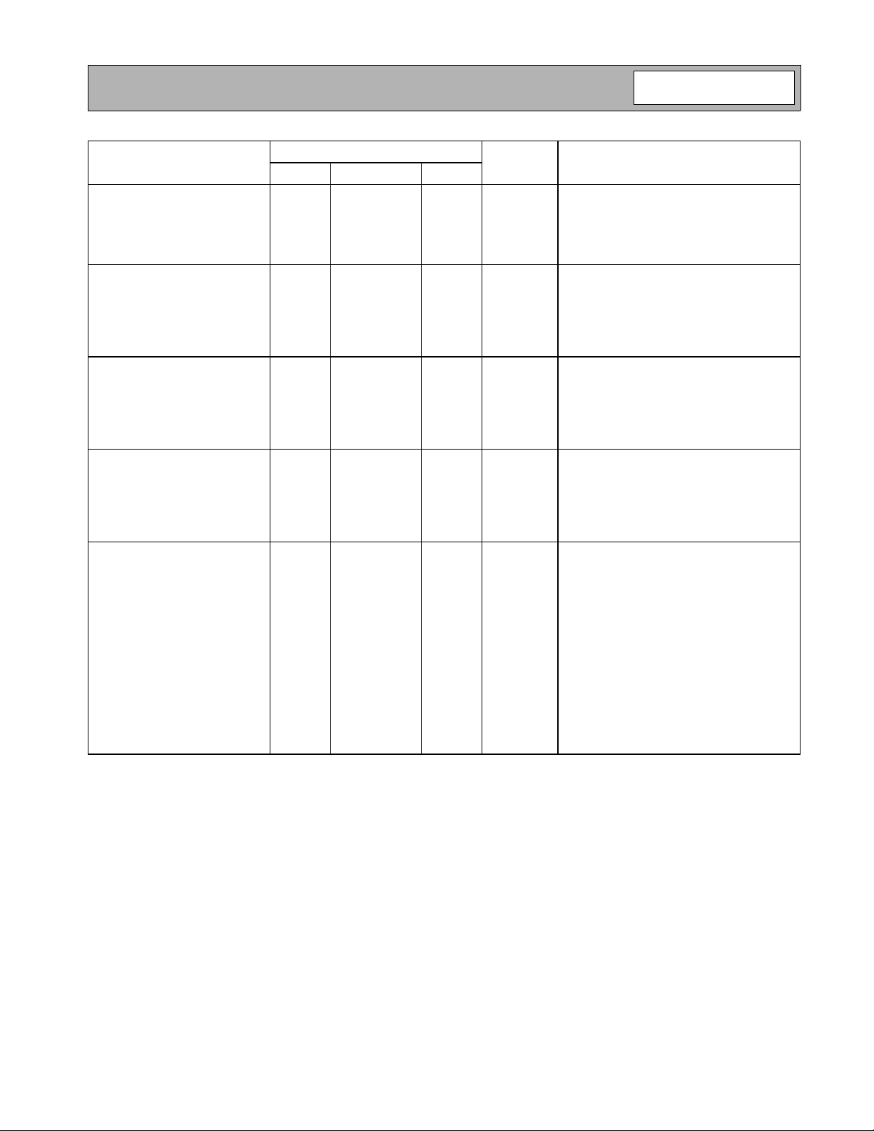
Absolute Maximum Ratings
Parameter Rating Unit
Supply Voltage +4.0 V
Input, Output or I/O Voltage Ground-0.5 to VCC+0.5 V
Voltage 2.7 to 3.6 V
VDDD Output 2.7 V
Max. Storage Temperature -65 to +150 °C
Max. Junction Temperature +150 °C
Operating Ambient Temperature -40 to +85 °C
DC
DC
DC
Caution! ESD sensitive device.
RF Micro Devices belie ves t he furnished inf ormation is correct and accur ate
at the time of this printing. However, RF Micro Devices reserves the right to
make changes to its products without notice. RF Micro Devices does not
assume responsibility for the use of the described product(s).
Parameter
Min. Typ. Max.
Specification
Unit Condition
See Figures 15 and 16.
=3.0V to 3.3V+10%,
DC Electrical
V
CC
= -40°C to +85°C
T
Z
Power Supply Voltage 2.7 3.3 3.6 V VDDA
TBD 2.2 TBD V VDDD, Output Only.
1.6 1.7 1.8 V No current draw.
V
REF
Input Voltage 2.5 VDDA+0.2 V Logical “1” (V
-0.2 +0.7 V Logical “0” (V
Output Voltage TBD VDDA-1.0 TBD V Logical “1” (V
TBD 0.2 0.7 V Logical “0” (V
Current Consumption 25 TBD mA Transmit Mode (I
50 TBD mA Receive Mode (I
IH
IL
OH
OL
)
)
)
)
)
TX
)
RX
Sleep Mode 500 500 µA Mode 1, Reset Active, No Clocks (I
1.5 1.5 mA Mode 2, Reset Inactive, No Clocks (I
Input Leakage Current 10 µAI
Output Leakage Current 10 µAI
I
O
Output Loading 20 20 pF
AC Electrical
VCC=3.0V to 3.3V+10%,
=-40°C to +85°C. See Note 1.
T
A
M CLK Duty Cycle 40/60 60/40 %
Rise/Fall - 10 nS All outputs. See Notes 2 and 3.
TXPE to I
OUT/QOUT
TXDATA to I/Q
OUT
3.0 3.1 µS 1st valid chip. 802.11 modes.
1.0 µS
TXPE Inactive Width 1 µS See Notes 2 and 4.
TXRDY Active to
500 nS
1st DATACLK Hi
Setup TXDATA to DATACLK 10 nS
Hold TXDATA t o DATACLK Hi 10 nS
Reset to TXPE 100 µS
Reset to RXPE 100 µS
TXDATA Modulation Extension 2 µS See Notes 2 and 5.
RXPE Inactive Width 0 nS See Notes 2 and 6.
DATACLK Period 90 nS 11Mbps Mode
DATACLK Width Hi or Low 22 44 68 nS 11Mbps Mode
DATACLK to RX Data 30 nS
RXRDY to 1st DATACLK 40 nS See Note 2.
RXDATA to 1st DATACLK 40 nS
Setup RXDATA to DATACLK 30 nS
RESET Width Active 40 nS See Note 2.
RXPE to CCA Valid 15 µS See Note 2.
RXPE to RSSI Valid 15 µS See Note 8.
to RXDATA 2.25 µS
I/Q
IN
S1
S2
)
)
11-322
Rev A4 031216
Page 3
RF3000
Parameter
Min. Typ. Max.
Specification
Unit Condition
I/Q ADC
Full Scale Input Voltage 0.7 +10% V
Input Bandwidth 11 MHz
Input Capacitance 5 pF
Input Impedance 5 0 kΩ
P-P
See Note 7.
I/Q DAC
Full Scale Output Voltage 200 mV See Note 7.
Sample Rate 11 MHz
Resolution 6 bits
DNL 0.5 LSB
INL 0.5 1.0 LSB Tested for monotonicity.
TX VGC DAC
Maximum Gain Output Voltage 1.2 V
Minimum Gain Output Voltage 2.0 V
Resolution 6 bits
DNL 0.5 LSB
INL 0.5 1.0 LSB Tested for monotonicity.
RX VGC DAC
Maximum Gain Output Voltage 1.2 V
Minimum Gain Output Voltage 2.0 V
Resolution 6 bits
DNL 0.5 LSB
INL 0.5 1.0 LSB Tested for monotonicity.
Control Port Timing
Characteristics
SPI Mode
C CLK Clock Frequency 6 MHz f
CS High Time Between
Transmissions
CS Falling to C CLK Edge 22 nS t
C CLK Low Time 68 nS t
C CLK High Time 68 nS t
CD IN to C CLK Setup Time 42 nS t
C CLK Rising to Data Hold Time 16 nS t
C CLK Falling to CD OUT Stable 47 nS t
1.1 µSt
Mode Switching Characteristics.
See Figure 3.
CLK
CSH
CSS
CLKL
CLKH
DSU
DHLD
PD
Notes:
1. AC tests performed with C
V
=0V; VOH=VOL=VCC/2.
IL
=20pF, IOL=2mA, and IOH=-1mA. Input reference level all inputs VCC/2. Test VIH=VCC,
L
2. Not tested, but characterized at initial design and at major process/design changes.
3. Measured from V
to VIH.
IL
4. TX PE must be inactive before going active to generate a new packet.
5. I
OUT/QOUT
are modulated after last chip of valid data to provide ramp-down time for RF/IF circuits.
6. A new search will begin after last bit of 802.11 packet in 802.11 modes.
7. Centered about 1.7V V
REF
.
8. Accurate to within ±3dB of final gain setting.
Rev A4 031216
11-323
Page 4

RF3000
For more information on Figure 1, see parameter table (on previous pages).
CSb
CCLK
CDIN
CDOUT
Figure 1. SPI Timing Transition Detail
ss
TXPE
TXRDY
DATACLK
TXDATA
ss
ss
ss
Figure 2. Transmit Port Detail Timing
ss
RXPE
RXRDY
DATACLK
RXDATA
ss
ss
ss
Figure 3. Receiver Port Detail Timing
11-324
Rev A4 031216
Page 5

Index
RF3000
GENERAL DESCRIPTION
Figure 4. 2.4GHz IEEE802.11b Chipset Diagram
Figure 5. RF3000 Block Diagram
SPI CONTROL PORT
SPI Mode Description
SPI Mode Pin Definitions Ta ble
SPI Method of Operation
Write
Read
SPI Operation Summary
Write
Read
SPI Mode Functional Timing Diagrams
Figure 6. SPI Write Functional Timing Diagram
Figure 7. SPI Read Functional Timing Diagram
METHOD OF OPERATION
IEEE802.11b Transmit Modes
IEEE802.11b DSSS Transmit Modes
IEEE802.11b DSSS Transmission Summary
Figure 8. IEEE802.11b Transmit Timing Overview
Figure 8a. Alternate Transmit Interface
IEEE802.11b Receive Mode
Diversity
Figure 9. Diversity and AGC Algorithm
AGC Algo rit hm
Figure 10. AGC Decision Structure
AGC Calibration
Figure 11. High Gain Mode (LNAGS=1) Plot of
RXVGC Showing Normal Operation and Calibration
Ranges
Figure 12. Low Gain Mode (LNAGS=0) Plot of
RXVGC Showing Normal Operation and Calibration
Ranges
High Gain Calibration Procedure
Low Gain Calibration Procedure
Post-AGC
IEEE802.11b DSSS Receive Summary
Figure 13. IEEE802.11b Receive Timing Overview
Figure 13a. Alternate Receiver Interface
BLOCK DIAGRAM BREAKOUT
Modulator
PSK Modes
CCK Mode
IEEE802.11b Preamble/Header Creation and
Assembly
Demodulator
PSK Modes
CCK Mode
IEEE802.11b Preamble/Header Detection and
Extraction
Data Converters
A/D Converters
D/A Converters
RSSI, CCA and AGC
Scramblers
Diversity
Equalizer
CONTROL PORT REGISTER DEFINITIONS FOR
RF3000
Register 0x0 - Reserved
Register 0x01 - Modem Control and RX Status
Mode 3-0 - TX Mode Table
Register 0x02 - CCA Control
CCA1, CCA0 - 802.11 CCA Mode Table
Register 0x03 - Diversity and RSSI Value
Register 0x04 - RX Sign al Field
Register 0x0 5 - RX Length Field MSB’s
Register 0x06 - RX Length Field LSB’s
Register 0x0 7 - RX Service Field
Register 0x08 - Reserved
Register 0x09 - Reserved
Register 0x0A - Reserved
Register 0x0B - Reserved
Register 0x0C - Reserved
Register 0x0D - Reserved
Register 0x0E - Reserved
Register 0x0F - Reserved
Register 0x10 - Reserved
Register 0x1 1 - TX Variable Gain and TX Length Field
Extension
Scrambler Mode Table
Register 0x12 - TX Length Field MSB’s
Register 0x1 3 - TX Len gth Field LSB’s
Register 0x1 4 - Low Gain Calibration
Register 0x15 - High Gain Calibration
Register 0x16 - Reserved
Register 0x17 - Reserved
Register 0x18 - Reserved
Register 0x19 - Reserved
Register 0x1A - Reserved
Register 0x1B - Reserved
Register 0x1C - Options Register 1
Register 0x1D - Options Register 2
Register 0x1E - Reserved
Register 0x1F - Reserved
Rev A4 031216
11-325
Page 6

RF3000
Pin Function Description Interface Schematic
1 TXPE
2RXPE
3MCLK
4TXRDY
5RXRDY
6VDDD
7GNDD
8 CCA
9LNAGS
10 TXDATA
11 DATACLK
12 RXDATA
13 CSb
14 CCLK
15 CDIN
16 CDOUT
17 RXVGC
18 NC
19 IIN
20 QIN
21 VDDA
22 GNDA
23 IOUT
24 QOUT
25 TXVGC
26 ANTSEL
27 RESET
28 VREF
Input from the external network processor. The rising edge of TX PE
places the transmitter into an active state. The falling edge of TX PE
indicates the end of transmission.
When active (value '1'), the receiver is powered up and CCA circuitry is
active.
Master clock. This should be a 44MHz for IEEE802.11b and is used to
generate other internally used clocks.
Indicates that the chip is ready to accept data from the MAC for Tx.
Indicates that the chip is ready to deliver data to the MAC from Rx.
Output from 2.2V internal voltage regulator for digital sections of
RF3000. This pin should not be connected to anything.
Ground signal for digital power.
Clear channel assessment per IEEE802.11b standard. “1” indicates
“clear”.
LNA gain select. “1” indicates “high gain”.
TX data stream input.
Data clock f or TX and RX data.
RX data stream output.
In SPI mode this pin serves as serial port chip select.
Serial port clock. This clock is used for SPI mode.
In SPI mode this pin serves as CDIN input.
In SPI mode this pin serves as CDOUT output.
Analog receive variable gain control output: 1.2V to 2.0V.
Not connected.
Analog I input.
Analog Q input.
DC power for analog sections 3.3V.
Ground signal for analog power.
Analog I output: 1.6V to 1.8V.
Analog Q output: 1.6V to 1.8V.
Analog voltage for transmitter variable gain control: 1.2V to 2.0V.
Antenna selection signal for diversity receiver.
Pin='1' chip reset.
Pin='0' standard operation.
Reference voltage for internal data converters.
Connect to RF2948 V
or set to 1.7VDC.
REF
11-326
Rev A4 031216
Page 7

General Description
RF3000
VREF
RXVGC
DAC
Q-IN
ADC
Data Converter
Reference
I-IN
ADC
TXVGC
DAC
I-OUT
DAC
Q-OUT
DAC
RF3000
CCA
Demodulator
Modulator
802.11
Preamble/
Header
Control
Port
Mode Control
802.11
Preamble/
Header
Tx Length
Tx Signal
Service
VGC
CCA
LNA GS
RX DATA
RX RDY
DATA CLK
SPI
TX RDY
TX DATA
RX PE
TX PE
MCLK
RX
Antenna 1
Filter
Fc = 2442
Mhz
Antenna 2
VREF_1
LNA
RX VGC
ANT Select
RX Q DATA
RX I DATA
TX VGC
TX I DATA
TX Q DATA
Gain
Select
RFMD 2.4 GHz WLAN
System Block Diagram
RF2948
RX
+45°
-45°
IF Amp
TX
SAW
Fc = 374 MHz
Base Band Amp.
Active Selectable LPF
= 1 MHz to 35 MHz)
(f
C
0-30 dB Gain
Filter
Σ
Filter
Selectable
LPF
Fc = 2442
MHz
RX
Dual Gain Modes
TX
÷2
PA
Driver
Fc = 2442
MHz
IF
VCO
RF
VCO
IF
T/R
Switch
Diversity
Switch
RF
Figure 4. 2.4GHz IEEE802.11b Chipset Diagram
Figure 4 shows the complete 2.4 GHz chipset, and where the RF3000 fits into the system. Figure 5 shows a simplified
block diagram of the RF3000. The RF3000 is a complete spread-spectrum transceiver, allowing PSK system operation.
The RF3000 performs all of the functions necessary to modulate a digital data source for transmission in a wireless environment. The RF3000: handles preamble and header generation and extraction; automatic gain control; clear channel
assessment; antenna diversity; and, implements an equalizer to handle multi-path events at high data r ates.
Rev A4 031216
11-327
Page 8

RF3000
Figure 5. RF3000 Block Diagram
RX VGC
ANT Select
I Input
VREF
Q Input
TX VGC
I Output
Q Output
RXVGC
DAC
I-IN
ADC
Data Converter
Reference
Q-IN
ADC
TXVGC
DAC
I-OUT
DAC
Q-OUT
DAC
RF3000
802.11
Preamble/
Header
Control
Port
Mode Control
802.11
Preamble/
Header
Rx
VGC
Tx Length
Tx Signal
Service
CCA
LNA GS
Rx Data
Rx RDY
Data CLK
SPI
Tx RDY
Tx Data
Rx PE
Tx PE
Mclk
CCA
Demodulator
Modulator
11-328
Rev A4 031216
Page 9

RF3000
SPI Control Port
The control port is used by the Media Access Controller (MAC) to set up and modify the multiple operation modes of the
RF3000. The port is set to SPI mode, with the R F3000 actin g as Slave. Note that if no setup information is programmed
into the RF3000's registers, it will default to a BPSK 1Mbps IEEE802.11b DSSS mode. If an IEEE802.11b mode is
selected in Register 1, other waveform registers are ignored and the appropriate, standards compliant features are
enabled (e.g., PN code, preamble/header, etc.). TX length is required for all IEEE802.11b modes.
All Registers, as defined in the Register Definition section of this datasheet, can be read in re al time throu gh this co ntro l
port. Selected registers, as indicated in the Register section are read-only.
The control port of the RF3000 contains a mode to automatically increment the register pointer, allowing reading or writing of adjacent bytes without the need to stop and restart control port access.
SPI Mode Description
SPI mode pin definitions.
Pin Name Description
CS Serial port chip select. A value of '0' is port enabled.
C CLK Control port-bit clock input from serial port master.
CD IN Serial data input to the RF3000. Data is clocked in on the rising edge of C CLK.
CD OUT Serial data output from the RF3000. Data is clocked out on the falling edge of C CLK.
SPI Method of Operation
Write:
To Write into a register of the RF3000, the accessing SPI master needs to simply bring CS
RF3000 (0100000
RF3000 are msb first. This should be followed by the Auto-increment-bit and the Memory address pointer (MAP), this is
an 7-bit value to indicate the initial address for the write process. Register data is to immediately follow the MAP. If the
Auto-Increment-bit is set RF3000 will continue to write data 1 byte at a time into the address pointed to by the MAP, and
increment the MAP after each byte. When the SPI Master is finished filling registers, it must raise CS
end.
Read:
Reading the contents of the RF3 000 internal registers, the pro cedure is actually a write proces s followed by the read.
The SPI Master must bring CS
RF3000, by placing the RF3000 base address (0100000
SPI Master must now set the Auto-increment-bit and initialize the 7-bit MAP to the value of the register to be read. The
user should raise CS
to lower CS
will begin outputting the register contents. As long as the CS
will auto-increment the MAP. When the RF3000 reaches Address 31, the MAP will be reset to Register 0 and the process
continues.
again, and readdress the RF3000 providing a '1' for the Read/Write-bit. Once this is completed the RF3000
) and provide a '0' for the Read/Write-bit. The user should note that all data transfers to/from the
2
low, to prepare the RF3000 to look for its address. The SPI Master now addresses the
) on the data bus and append a '0' for the Read/Write-bit. The
2
, to end the write portion of the cycl e. To complete the Write/Read cycle th e SPI Master now needs
remains low, and the auto-increment bit is set, the RF3000
low, then Address the
to indicate the cycle
Rev A4 031216
11-329
Page 10

RF3000
SPI Operation Summary
To Write:
9. Bring CS
10.Chip Address (7-bits) - This should match the RF30 00 chip address of 0100000
11.Read/Write-bit = '0'
12.Auto-Increment-bit - Value of '1' enables auto-increment
13.Memory Address Pointer (MAP) (7-bits) - This is the address of the register to be written to, MSB first.
14.Register Data (8-bits) - MSB Firs t
15.Repeat step 6 if Auto-Increment or bring CS
To Read:
1. Bring CS
2. Chip Address (7-bits) - This should match the RF3000 chip address of 0100000
3. Read/Write-bit = '0'
4. Auto-Increment-bit - Value of '1' enables auto-increment
5. Memory Address Pointer (MAP) (7-bits) - This is the address of the register to be written to, MSB first.
6. Bring CS
7. Bring CS
8. Chip Address (s ame as step 2) - MSB First
9. Read/Write-bit = '1'
10. RF3000 will output 8-bit register value, MSB First, and Increment MAP, if Auto increment enabled.
11. Repeat step 10 for polling or Auto-Increment or bring CS
low.
low.
high.
low.
HIGH to end operation.
high to end operation.
.
2
.
2
SPI Mode Functional Timing Diagrams
Write
CS
CCLK
CDIN
CDOUT
Chip Address
AI
Figure 6. SPI Write Functional Timing Diagram
Read
CS
CCLK
CDIN
CDOUT
Chip Address
Memory Address
"Hi Z"
Figure 7. SPI Read Functional Timing Diagram
Memory Address
"Hi Z"
Data Data
Chip Address
Data
"Hi Z"
11-330
Rev A4 031216
Page 11
RF3000
RF3000 Method of Operation
The transmitter power enable (TX PE) input enables the transmitter process. (Note: Transmit has prio rity over receive.)
When TX PE is high, the LNA GS signal will be driven low. The TX RDY output indicates the readiness of the RF3000 to
receive data for transmit. Transmitted data is passed into the RF3000 through the TXDATA input and clocked by the
DATA CLK output. The receiver power enable (RX PE) input enables the receiver, and the receive data ready (RX RDY)
signal indicates that received data is upcoming. The RF3000 generates the received data clocks, and outputs the
received data, through the RX DATA output. The receiver port also provides a clear channel assessment (CCA) to the
MAC.
The table below summarizes the operation of the chip. The user should note that RX PE must be High to perform CCA.
TX PE RX PE Operation
0 0 Standby mode.
0 1 RX is powered up. CCA circuity is active.
1 0 TX is powered up. Begin TX. CCA is inactive.
1 1 RESERVED
IEEE802.11b Transmit Modes
IEEE802.11b DSSS Transmit Modes
The RF3000 supports PSK and CCK DSSS modes defined in IEEE802.11b specification. The RF3000 also supports the
optional short preamble and header format as defined in IEEE802.11b.
The following section describes IEEE802.11b DSSS data transmission. The user must first prepare the applicable control port registers to deter mine the mode of operation and the transm ission length. The mode of ope ration must be wr itten into Register 1, followed by setting the transmission length (in microseconds). The length is to be written into
Registers 17 (bit 0 only), 18 and 19. Mode byte values for IEEE802.11b modes are summarized below
.
IEEE802.11 DSSS Mode Mode Byte Value
1Mbps DBPSK 0x00
2Mbps DQPSK Long preamble 0x20
2Mbps DQPSK Short preamble 0x30
5.5Mbps CCK Long preamble 0x40
5.5Mbps CCK Short preamble 0x50
11Mbps CCK Long preamble 0x60
11Mbps CCK Short preamble 0x70
16
16
16
16
16
16
16
Once the control por t values are written, the RF3000 is ready to transmit data. Optionally, the TX length value can be
written during the 128µS of preamble. When the user is ready to transmit, TX PE is driven High. This signals the RF3000
to assemble and transmit the 802.11 preamble and header, as described below.
Preamble Header Data
128 1’s SFD
(16-bits)
Service
(8-bits)
Signal
(8-bits)
Length
(16-bits)
CRC
(16-bits)
Data
(x-bits)
The preamble and header for 1 Mbps mode is always transmitted as 1 Mbps BPSK. However for 2 Mbps, 5.5 Mbps a nd
11 Mbps modes, IEEE802.11b allows a short preamble, which has the preamble, transmitted as 1Mbps BPSK and the
header transmitted as 2Mbps QPSK. The usage of the optional short preamble is selected when the transmission mode
is written to the control port.
Rev A4 031216
11-331
Page 12

RF3000
The RF3000 signals that it is nearing the end of the preamble and header transmission by driving TX RD Y high. This signals the user that transmission data clocks are coming. When the RF3000 is ready to transmit data it will begin clocking
transmit data. Data to be transmitted should be presen t on TX DATA on the rising edge of DATA CLK. The RF3000 will
only clock in the number of data-bits to fill the specified transmission time.
IEEE802.11b DSSS Transmission Summary
1. TX Mode different:
Write value to the mode register according to table.
2. TX Length different:
Write the number of uS to transmit in the TX length registers.
3. Drive TX PE High and wait for TX RDY to go High.
4. Transmit data must be valid on the rising edge of DATA CLK.
Figure 8 shows the primary interface mode for the RF3000 TX Data port.
CCA
RX PE
TX PE
TX RDY
DATA CLK
TX DATA
TX I
TX Q
Preamble
and Header
Rate Determined from Control Port Register 1
Data
Figure 8. IEEE802.11b Transmit Timing Overview
The RF3000 has provision for an alternate Transmit Data port interface. In the transmit interface an extra clock is
asserted after TXRDY goes ‘high' and before the first TX data clock on DATA CLK, see Figure 8a. The alternate Transmit
interface is enabled by writing 0x08 into RF3000 Register 0x1C.
CCA
RX PE
TX PE
TX RDY
DATA CLK
TX DATA
TX I
TX Q
Preamble and
Header
Rate Determined from Control Port Register 1
Data
Figure 8a. Alternate Transmit Interface
11-332
Rev A4 031216
Page 13

RF3000
IEEE802.11b Receive Mode
The RF3000 receiver has an interface similar to the transmit port, and provides link support data through the control port.
The user drives RX PE High to enable the receiver circuitry. The RF3000 then begins to w a tch the incoming data stream
for a valid Barker code PN sequence.
The RF3000 contains logic to perform AGC when used in c onjunction with the RF294 8 and RF2494 as in the RF031X
reference designs for I EEE802.11b. The follo wing secti ons will explain the method of AGC and the calibration hooks that
exist inside the RF3000 to compensate for manufacturing tolerances in total system gain of an IEEE802.11b radio.
Diversity
The RF3000 makes diversity decisions every 1mS while looking for A/D saturation according to the state machine in Figure 9.
NOT Saturated
Saturated
NOT Acquired
ANTSEL = 0
ANTSEL = 1
NOT Saturated
Saturated
AGC Algorithm
(Course Gain)
Wait 15 uS
Acquired
Demodulation
(Fine Gain)
Figure 9. Diversity and AGC Algorithm
AGC Algorithm
The RF3000 AGC algorithm is implemented to automatically control both the RXVGC of the RF2948 and the LNAGS pin
of the RF2494. The RF3000 is programmed to search the possible gain settings of LNAGS and RXVGC in a binary fashion to quickly determine the final gain setting needed to optimize the inputs to the A/D converters for demodulation. The
AGC algorithm is completely controlled by detection of saturation of the A/D converters.
Rev A4 031216
11-333
Page 14

RF3000
The RF3000 begins the algorithm by setting the RXVGC and LNAGS pins to a predetermined maximum gain co ndition.
Upon detection of A/D saturation, the RF3000 will decrease the system gain (via the RXVGC pin) to a predetermined
“mid-point”. This mid point is chosen to allow the RF3000 to determine the correct setting of the LNAGS pin. If the
RF3000 detects saturation at this “mid-point”, the RF3000 will place the RF front end into a low gain mode, and will begin
searching for the correct RXVGC setting in a binary tree fashion. If the RF3000 does not detect saturation on the A/D
converters while at this “mid-point”, the RF3000 will leave the LNAGS pin in high gain mode and proceed with the binary
search of RXVGC. This binary tree representation of the gain algorithm c an be seen in Figure 9. It is impor tant to note
that once the RF3000 makes a decision on the LNAGS setting, that setting will remain for the entire duration of the
packet and cannot be altered until the next packet.
Gain (VGC, LNAGS)
Max Gain
HIGH GAIN
LNA GS=1
Solid Lines are shifted
along the Gain axis
with adjustment of
Register 0x15
LOW GAIN
LNA GS=0
Time(t)
Min Gain
Dashed Lines are shifted
along the Gain axis
with adjustment of
Register 0x14
Indicates decision points
t=0 1uS 2uS 3uS 6uS
...
Figure 10. AGC Decision Structure
RSSI is a function of RXVGC and LNAGS. RSSI is updated every 1 µS dur ing the AGC algorithm. While demodulating
data, the demodulator will make fine tuning adjustments to RSSI based on the value of RXVGC.
An optional AGC algorithm is available, enabled by writing a '1' into bit 4 of Register 0x1C. In this mode the AGC may be
kicked off after it has already settled if a large signal is present. This addres ses a scena rio in w hich an interferer (which
may be noise) initially kicks off the AGC. The AGC then chooses the gain setting to acco mmodate this level of signal.
Subsequently, a desired signal is incident on the antenna. This signal may be larger than the interferer and, because of
the gain setting of the radio, may be difficult to demodulate. Under the optional AGC mode, the gain would be re-optimized to the desired signal. We believe that this will help radio performance in many environments. When using the new
AGC algorithm, Register 0x1C should be written to 0x78. The values of 0, 1, 1 in b7, b6, b5 respectively increases the
saturation requirement for the AGC algorithm. This has the effect of biasing the algor ithm to produce a higher gain se tting to give the baseband processor an optimum input amplitude for robust demodulation.
11-334
Rev A4 031216
Page 15

RF3000
Another optional mode has been added to the AGC algorithm. This mode adds a delay into the algorithm after the LNA
gain select is changed to allow enough time for the radio to settle properly. The delay eliminates the possibility of a 'dead
zone' where there is a small range of input power le vels with a probability that the AGC will settle to an incorrect gain setting. To enable this mode, Register 0x1 D is written to 0x80. In addition, the 6 lsb's of reg20 must be set to 4 higher the 6
lsb's of reg21 because the outcome of the AGC decision step will change. If this mode is no t to be used, Register 0x 1D
should be written to 0x00.
AGC Calibration
The RF3000 is preprogrammed for a “typical” radio. The default settings of the RF3000 may be used without modification, but the conditions of the AGC algorithm may be modified b y writing to register 21 and register 20 of the control port.
Register 21 controls an offset to the RXVGC DAC for LNAGS =1 (high gain mode), and register 20 con trols an offset to
the RXVGC DAC for LNAGS= 0 (low gain mode). Caution should be taken when setting these regis ters; incorrect settings can create a “dead zone” between th e high/low gain trees. The following figure shows the “typical” setting s for the
RXVGC output of the RF3000 during LNAGS =1. Also shown are th e expected production variances of an IEEE802.11
radio, and the calibration ranges of the RF3000. Writing to register 21 of the RF3000 will move the range of AGC operation on the RXVGC pin. For example, if the six LSB's in register 21 are written to 000100b (4 decimal), the starting po int
for the AGC algorithm (max gain) will be with a DAC code of 8+4=12 codes, and the LNAGS decision will be made at a
code of 47+4=51 codes. This has the overall effect of decreasing the gain provided by the RF2948 by four D/A codes or
approximately 5dB for both initial AGC setting for detection of saturation and for determining LNAGS. Likewise if the six
LSB's of register 21 are written to 1111000 (-4 decimal) , the initial condition that the RF 3000 uses to look for saturation
is 8-4=4 codes, and the LNAGS decision is determined at 47-4=43 codes.
D/A Code
Typical
RF2948
Gain
Process
Variation
Cal Range Cal Range
Typical RF3000 AGC Range
0 63824 3947
67.8dB 21.7dB
Process
Variation
Figure 11. High Gain Mode (LNAGS=1) Plot of RXVGC Showing Normal Operation and Calibration Ranges
Similar to the high gain calibration, register 20 controls an offset into the LNAGS =0 (low gain mode) values that are
applied to the D/A converter. The figure below shows the normal operation range of the RF3000 and the calibration
range that is provided.
D/A Code
Typical
RF2948
Gain
Process
Variation
Cal Range Cal Range
Typical RF3000 AGC Range
0 63817 3954
67.8dB 13.4dB
Process
Variation
Figure 12. Low Gain Mode (LNAGS=0) Plot of RXVGC Showing Normal Operation and Calibration Ranges
Rev A4 031216
11-335
Page 16

RF3000
High Gain Calibration Procedure
Calibration of an IEEE802.11b radio can be accomplished by sending a repetitive pattern to the radio at a known input
power, and adjusting the register settings until all packets are correctly received without errors or missing packets. A simple procedure is contained outlined as follows.
1. Write the six LSB's of register 21 to the value 011000 (24 decimal). This will decrease the total system gain.
2. Apply an 1Mbps IEEE802.11b signal to the input of the radio of a known input power (-75dBm).
3. Decrease the si x LSB's of register 21 by one LSB until all packets are received correctly without dropping any pack-
ets.
4. Since the input power of the reference signal was set to -75dBm (to eliminate effects of thermal noise), calculate the
final register 21 setting by subtracting a known predetermined value from the value found in step 3 of the calibration
procedure.
Low Gain Calibration Procedure
Similar techniques can be applied to calibrate the Low gain settings of the RF3000. As an initial value, the register setting in register 20 should be equal to the value of register 21. Register 20 is provided to allow manufacturing calibration
to account for reverse isolation variances in the T/R switch if used as an additional pad.
Post-AGC
When the Barker code is acquired, the R F3000 a ssigns the ACQ-bit in the mode r egister to a 1 an d proce eds to extract
the header information. When the start frame delimiter is identified, the RF3000 will assign a 1 to the SFD-bit in the
mode register. The RF3000 will now decode the transmission mode and data length from the header, and check the
header via the 16-bit CRC. The RF3000 will then clock-out 32 bits of header information. This will be the 8-bit RX signal
field, followed by the 8-bit RX service field, and then the 16-bit RX length field. The MAC can also read these values
through the serial port registers 0x04 through 0x07.
The header data will be followed by 16 bit times of no clock transitions.
Immediately before providing data, the RF3000 will drive RX RDY High. The received data will be stable on the rising
edge of DATA CLK
packet, but no DATA CLK or RX DATA transitions will occur.
. In the event the header CRC is incorrect, the RF3000 will bring RX RDY high for the duration of the
11-336
Rev A4 031216
Page 17

RF3000
IEEE802.11b DSSS Receive Summary
1. Drive RXPE High.
2. RF3000 look s for incoming valid Barker Code.
3. RF3000 sets ACQ bit in Register 0x01.
4. When the Start Frame Delimiter is identified, the RF3000 sets the SFD bit in Register 0x01.
5. RF3000 Extracts Header information.
This information is copied into the RF3000 RX Status, Service fields and presented on the RXDAT A Pin with Cloc ks on
DATA CLK.
6. This will be followed by 16 bit times of no clock transitions.
7. RF3000 Drives RXRDY high, and clocks Received Data on the rising edge of DATA CLK.
8. RF3000 Drives RXRDY low at the end of the data packet.
RXPE
RXRDY
DATACLK
RXDATA
32CLK
Cycles
Header
Data
Preamble and
Header
Extraction
Rate Determined from Received IEEE802.11 Signal Field
Data
Figure 13. IEEE802.11b Receive Timing Overview
The RF3000 has provision for an alternate Receive Data port interface. In the receiver interface, the DATACLK is
inverted, and an extra clock is asserted after RXRDY goes 'low' indicating the end of the received packet, see Figure
13a. The alternate Transmit interface is enabled by writing 0x08 into RF3000 Register 0x1C.
RXPE
RXRDY
DATACLK
RXDATA
32CLK
Cycles
Header
Data
Preamble and
Header
Extraction
Rate Determined from Received IEEE802.11 Signal Field
Data
Figure 13a. Alternate Receiver Interface
Rev A4 031216
11-337
Page 18

RF3000
Block Diagram Breakout
The following sections describe each of the blocks, as indicated in the block diagram, that comprise the RF3000.
Modulator
PSK Modes
The RF3000 uses a proprietary architecture that allows the modulation of PSK signals by simply reprogramming the part
via the control port. The transmitte d data stream is first spread and the resulting data stream is modulated.
CCK Mode
IEEE802.11b Preamble/Header Creation and Assembly
The RF3000 provides circuitry to generate and as se mble a preamble and header as specified in the IEEE802.11b specification. The short preamble option for 2 Mbps, 5.5Mbps and 11Mbps, as specified in IEEE802.11b, is selectable in the
mode control register. The RF3000 will transmit these fields along with a protective CRC-16 for error detection. For other
protocols, the preamble/header circuitry is disabled, and packet structures should be generated externally.
Demodulator
PSK Modes
The RF3000 uses a proprietary architecture that allows the demodulation of PSK signals by simply reprogramming the
part via the control port. The received signal is first de-spread and the PSK signal is recovered.
CCK Mode
In order to perform CCK demodulation, circuitry is provided to pass the output of the A/D converters to a fast Walsh
transform (FWT). The output of the FWT is then passed to decision circuitry to determine the received signal.
IEEE802.11b Preamble/Header Detection and Extraction
Circuitry is provided to search the in coming data for start frame delimiter (SFD) and to obtain length field information as
well as modulation type. In 802.11 modes, this circuitr y is always active since the preamble and header tells the PHY
which modulation type the data packet is using. The RF3000 will also check the preamble/header field for errors by
checking the CRC-16 field for errors.
Data Converters
The RF3000 contains all A/D converters and D/A converters required to implement a transceiver.
A/D Converters
I/Q A/Ds - These are 4-bit analog-to-digital converters used to sample the data according to the mode of the RF3000.
D/A Converters
Four (4) digital-to-analog converters are present for transmitter VGC, receiver VGC, I Out, and Q Out.
RSSI, CCA and AGC
Scramblers
Scramblers for whitening the spectrum are provided, as specified in IEEE802.11b.
SCRAMBLER NOTE: The data scrambler defined by IEEE802.11b has a probability of 1/128, to lock up scrambling
when random data is followed by a repetitive pattern. The patterns identified are: all 0's ; all 1’s; repetitive 01's; repeated
0011's; and, repeated 000111's. Once the pattern ceases the scrambler will resume its normal operation.
11-338
Rev A4 031216
Page 19

RF3000
Diversity
Switching and detection at beginning of Receive.
Equalizer
Proprietary architecture, active only in 5.5Mbps and 11Mbps CCK modes. For multipath cancellation, the RF3000
defines the path with the largest magnitude as the main pa th and all others as seco ndar y paths. The RF3000 equa lizer
can cancel the two most sign ificant secondary paths. these can either be two (2) post-cursor , echo paths, or they ca n b e
one (1) post-cursor and one (1) p re-curs or path s. Pre-cursor delay can be up to on e-qu arter symbol period. Post-cursor
delay can be up to one (1) symbol period. The magnitude of cancelled multipaths up to -3 dBc, norm alized to the main
path.
Rev A4 031216
11-339
Page 20
RF3000
Control Port Register Definitions for RF3000
Register 0x00 - Reserved
R7 R6 R5 R4 R3 R2 R1 R0
This register is reserved.
Register 0x01 - Modem Control and RX Status
Mode 3 Mode 2 Mode 1 Mode 0 Short Preamble* ACQ * SFD * CRC *
* - Read Only
This register is used to setup primary operation of the modem.
NOTE: The four (4) LSB’s are read-only and reflect the receiver status.
Mode (3-0) - TX Mode
Mode 3 Mode 2 Mode 1 Mode 0 Mode ID Notes
0000802.11 1Mbps DSSSDefault Mode
0001Reserved Reserved
0010802.11 2Mbps DSSSLong preamble
0011802.11 2Mbps DSSSShort preamble
0100802.11 5.5Mbps CCKLong preamble
0101802.11 5.5Mbps CCKShort preamble
0110802.11 11Mbps CCKLong preamble
0111802.11 11Mbps CCKShort preamble
1000BPSK Reserved
1001QPSK Reserved
1010Reserved Reserved
1011Reserved Reserved
Default 802.11 1Mbps DSSS, RX mode detected automatically.
NOTE: In 802.11 modes, the received data rate will be accepted from the received header and therefore will be selected
automatically.
Short Preamble - READ ONLY
0 - Long Preamble Received
1 - Short Preamble Received
ACQ - Receiver acquisition status - READ ONLY
0 - Not locked
1 - acquired
SFD - 802.11 SFD status - Read Only
0 - Not found
1 - SFD detected
CRC - 802.11 RX CRC - Read Only
0 - CRC valid
1 - CRC error
11-340
Rev A4 031216
Page 21
Register 0x02 - CCA Control
CCA1 CCA0 RSSI_t5 RSSI_t4 RSSI_t3 RSSI_t2 RSSI_t1 RSSI_t0
CCA1, CCA0 - 802.11 CCA Mode:
CCA1 CCA0 CCA Mode
0 0 RSSI Threshold Sensitive
0 1 Acquisition Sensitive
1XBoth
RSSI_t - 6-bit RSSI threshold value for CCA.
Register 0x03 - Diversity and RSSI Value
Diversity Cpantsel RSSI5 * RSSI4 * RSSI3 * RSSI2 * RSSI1 * RSSI0 *
* - Read Only
NOTE: The six (6) LSB’s are read-only and reflect the receiver status.
Diversity - RX diversity enable bit.
Default - 0
0 - No diversity, ANT SEL pin is forced to Cpantsel.
1 - Diversity active, RF3000 automatically selects ANT SEL pin.
Cpantsel - Antenna selection bit in non-diversity mode.
Default - 0
0 - ANT SEL forced to 0.
1 - ANT SEL forced to 1.
RSSI5-0 - Output of the RSSI A/D - Read Only
RF3000
Register 0x04 - RX Signal Field (Read only)
RX_Sig7 RX_Sig6 RX_Sig5 RX_Sig4 RX_Sig3 RX_Sig2 RX_Sig1 RX_Sig0
In DSSS modes, this value is the received byte of the received signal field. In FHSS, only the four (4) LSB’s are used.
BIT 7 BIT 6 BIT 5 BIT 4 BIT 3 BIT 2 BIT 1 BIT 0 Received Mode
000010101Mbps DSSS
000101002Mbps DSSS
001101115.5Mbps DSSS
0110111011Mbps DSSS
00000000Reserved
000000011.5Mbps FSK***
00000010Reserved
000000112.5Mbps FSK***
000001003Mbps FSK***
000001013.5Mbps FSK***
000001104Mbps FSK***
000001114.5Mbps FSK***
*** - IEEE802.11b proposed modulation rates not currently supported.
Register 0x05 - RX Length Field MSB’s (Read only)
RX_LN15 RX_LN14 RX_LN13 RX_LN12 RX_LN11 RX_LN10 RX_LN9 RX_LN8
The upper byte of the length field received.
In DSSS mode, this value is the length in microseconds of the received data packet.
Rev A4 031216
11-341
Page 22
RF3000
Register 0x06 - RX Length Field LSB’s (Read only)
RX_LN7RX_LN6RX_LN5RX_LN4RX_LN3RX_LN2RX_LN1RX_LN0
The lower byte of the length field received.
Register 0x07 - RX Service Field (Read only)
RX_SER7 RX_SER6 RX_SER5 RX_SER4 RX_SER3 RX_SER2 RX_SER1 RX_SER0
This register is used per IEEE802.11b specification.
RX_SER7 is length field extension in high data rate proposal 802.11b.
RX_SER3 is modulation selection bit for high rate transmission.
0 - CCK
RX_SER2 signifies Synth Clock to Signal Clock per 802.11 specification.
Register 0x08 - Reserved
Register 0x09 - Reserved
Register 0x0A - Reserved
Register 0x0B - Reserved
Register 0x0C - Reserved
Register 0x0D - Reserved
Register 0x0E - Reserved
Register 0x0F - Reserved
Register 0x10 - Reserved
Register 0x11 - TX Variable Gain and TX Length Field Extension
TXVGC5 TXVGC4 TXVGC3 TXVGC2 TXVGC1 TXVGC0 SCRAMBLER TX_LN16
TXVGC5-TXVGC0 - Gain setting for transmission.
000000 - Min gain
111111 - Max gain
SCRAMBLER - This bit enables and disables the IEEE802.11b data scrambler.
Bit Value Scrambler Mode
0 Enabled
1 Disabled
TX_LN16 - TX length extension bit as defined in IEEE 802.11b specification.
Register 0x12 - TX Length Field MSB’s
TX_LN15 TX_LN14 TX_LN13 TX_LN12 TX_LN11 TX_LN10 TX_LN9 TX_LN8
Register 0x13 - TX Length Field LSB’s
TX_LN7 TX_LN6 TX_LN5 TX_LN4 TX_LN3 TX_LN2 TX_LN1 TX_LN0
Registers 0x12 and 0x13 indicate the number of microseconds that the RF3000 is to transmit after receiving a request to
start transmission.
11-342
Rev A4 031216
Page 23

RF3000
Register 0x14 - Low Gain Calibration
Reserved Reser ved Low_Gain5 Low_Gain4 Low_Gain3 Low_Gain2 Low_Gain1 Low_Gain0
Bit 5 .. Bit 0:Low Gain Calibration, Range -32 to +16
Register 0x15 - High Gain Calibration
Bit 7 Bit 6Bit 5Bit 4Bit 3Bit 2Bit 1Bit 0
Channel 14 Filter DSSS PAD High_Gain5 High_Gain4 High_Gain3 High_Gain2 High_Gain1 High_Gain0
Bit 7: A value of ‘1’ enables the channel 14 filter
Bit 6: 6dB pad of DS modes
Bit 5 .. Bit 0:High Gain Calibration, Range -8 to +31
Register 0x16 - Reserved
Register 0x17 - Reserved
Register 0x18 - Reserved
Register 0x19 - Reserved
Register 0x1A - Reserved
Register 0x1B - Reserved
Register 0x1C - Options Register 1
Bit 7 Bit 6 Bit 5 Bit 4 Bit 3 Bit 2 Bit 1 Bit 0
SAT_THRESH [2] SAT_THRESH [1] SAT_THRESH [0] ALT AGC Enabled Alternative
Data Port Interface
Bit 7 .. Bit 5:Signed Magnitude Offset for all steps of course AGC. Saturation threshold is 4+ value where V=3<
RESERVED ’0’ RESERVED ‘0’ RESERVED ‘0’
Value<3.
Bit 4: A value of ‘1’ allows the AGC algorithm to retrigger with ADC saturation.
Bit 3: A value of ‘1’ enables the alternate TX/RX data bus interface.
Bit 2: Reserved, set to ‘0’.
Register 0x1D - Options Register 2
Bit 7 Bit 6 Bit 5 Bit 4 Bit 3 Bit 2 Bit 1 Bit 0
LNAGS DELAY R ESERVED ‘0’ RESERVED ‘0’ RESERVED ‘0’ RESERVED ‘0’ AGC Re-trigger
Threshold
RESERVED ‘0’ RESERVED ‘0’
Bit 7: LNAGs Delay-When set to ‘1’, this delays the ne xt A GC decision step an extr a 1µS (total of 2µS) if a transition
of the LNAGs pin from 1 to 0 occurs.
Bit 6 .. Bit 3:Reserved, set to ‘0’.
Bit 2: Sets threshold for AGC re-trigger.
‘0’ sets re-trigger threshold to high count.
‘1’ sets re-trigger threshold to low count.
Bit 1: Reserved, set to ‘0’.
Bit 0: Reserved, set to ‘0’.
Register 0x1E - Reserved
Register 0x1F - Reserved
Rev A4 031216
11-343
Page 24

RF3000
Pin Out
MCLK
TXRDY
RXRDY
VDDD
1TXPE
2RXPE
3
4
5
6
7GNDD
8CCA
9LNAGS
10TXDATA
11DATACLK
12RXDATA
13CSb
28 VREF
27 RESET
26 ANTSEL
25 TXVGC
24 QOUT
23 IOUT
22 GNDA
21 VDDA
20 QIN
19 IIN
18 NC
17 RXVGC
16 CDOUT
15 CDIN14CCLK
11-344
Rev A4 031216
Page 25

J1
MCLK
MCLK
GNDD
J2
Q OUT
Q OUT
E22
GNDA
J3
I OUT
I OUT
E23
GNDA
J4
Q IN
Q IN
E24
GNDA
J5
I IN
I IN
E25
GNDA
P3 Power
123
4
GNDA GNDD
VREF
5.0 VCC
R5
0 Ω
GNDA GNDD
C3
0.47 µF
RF3000
Evaluation Board Schematic
(Download Bill of Materials from www.rfmd.com.)
P1
MCLK
E1
RESET
TXVGC
QOUT
IOUT
GNDA
3.3VCC
Q IN
RSSI
RXVGC
CDOUT
CDIN
GNDD
R3
10 kΩ
VREF
C4
0.1 µF
C2
R1
0.47 µFC110 nF
0 Ω
I IN
R2
4.7 kΩ
3.3 VCC
E14
E15
E18
E21
E19
C7
0.01 uF
4.7 uF
CCA
TXRDY
RXRDY
RXPE
TXPE
5.0 VCC
5.0 VCC
C6
U1
TXPE
1TXPE
RXPE
RXPE
2
MCLK
MCLK
3
TXRDY
TXRDY
E10
RXRDY
VDDD
GNDD
CCA
LNA CNTL
TXDATA
DATACLK
RXDATA
CS
CCLK
4
RXRDY
5
VDDD
6
GNDD
7
CCA
8
LNA CNTL
9
TXDATA
10
DATACLK
11
RXDATA
12
CSN AD0
13
CCLK
RF3000
P2
Analog I/O
12345
VREF
E20
TXVGC
ANTSEL
E16
E13
ANTSEL
RSVGC
CDOUT SDA
CDIN AD1
RSSI
RXVGC
E9
E5
VREF
RESET
TXVGC
QOUT
IOUT
GNDA
VDDA
Q IN
RSSI
I IN
28
27
ANTSEL
26
25
24
23
22
21
20
19
18
17
16
1514
3000400, Rev. B
P2
2
P3
3
P4
4
P5
5
P6
6
CE1
7
8
P8
9
OE
10
P10
P11
11
P12
12
P13
13
P14
WE:P
15
READY
16
5.0 VCC
17
VPP
18
P19
19
P20
20
P21
21
P22
22
P23
23
24
P24
25
P25
26
P26
27
P27
28
P28
29
P29
30
P30
31
P31
32
P32
33
WP
34
GND
PCMCIA CON
U2
BYPASS
1 8
NC
2
GND
3
INPUT
4
LP2987
GND
1
GND
REFRESH
I/ORD
I/OWR
5.0 VCC
VPP2
RESET
WAIT
INPACK
SPKR
STSCHG
GND
SHTDN
ERROR
SENSE
OUTPUT
CD1
CE2
VS2
REG
CD2
35
36
LNA CNTL
TXDATA
DATACLK
RXDATA
CCLK
CDOUT
CDIN
5.0 VCC
RESET
E12
E6
E11
E3
CS
E7
E2
E8
E4
E17
GNDDGNDD
R4
330 kΩ
C5
4.7 uF
37
P37
38
P38
39
P39
40
P40
41
P41
42
43
44
45
46
P46
47
P47
4814
P48
49
P49
50
P50
51
52
53
P53
54
P54
55
P55
56
P56
57
58
59
60
61
62
63
64
P64
65
P65
66
P66
67
68
3.3 VCC
7
6
5
Rev A4 031216
11-345
Page 26

RF3000
Evaluation Board Layout
Board Size 2.12” x 3.57”
Board Thickness 0.062”, Board Material FR-4
11-346
Rev A4 031216
Page 27

RF3000
Rev A4 031216
11-347
Page 28

RF3000
11-348
Rev A4 031216
 Loading...