

Datasheet REG103UA-5, REG103UA-5-2K5, REG103UA-A, REG103UA-A-2K5, REG103FA-A-500 Datasheet (Burr Brown)
...Page 1
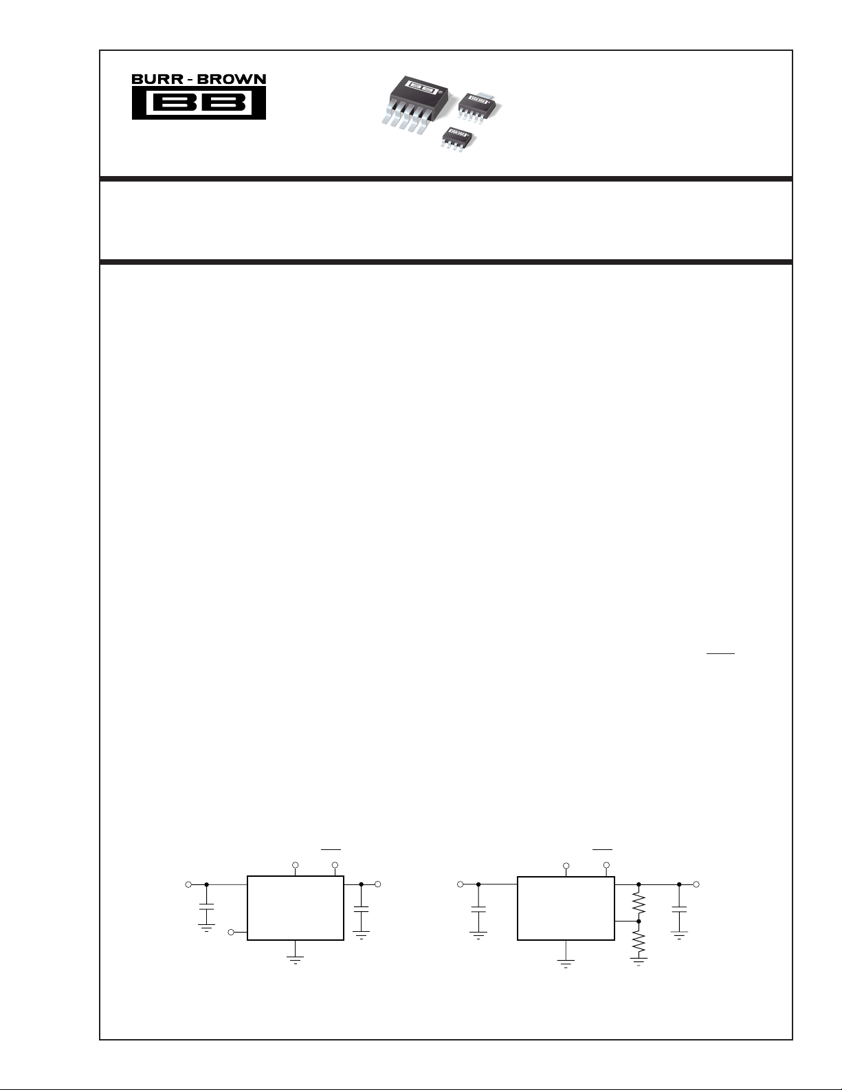
®
For most current data sheet and other product
information, visit www.burr-brown.com
500mA Low Dropout Regulator
REG103
REG103
REG103
DMOS
REG103
FEATURES
● NEW DMOS TOPOLOGY:
Ultra Low Dropout Voltage:
115mV typ at 500mA and 3.3V Output
Output capacitor NOT required for stability
● FAST TRANSIENT RESPONSE
●
VERY LOW NOISE:
33µVrms
● HIGH ACCURACY: ±2% max
● HIGH EFFICIENCY:
I
= 1mA at I
GND
Not Enabled: I
= 500mA
OUT
= 0.5µA
GND
● 2.5V, 2.7V, 3.0V, 3.3V, 5.0V AND
ADJUSTABLE OUTPUT VERSIONS
● FOLDBACK CURRENT LIMIT
● THERMAL PROTECTION
● OUTPUT VOLTAGE ERROR INDICATOR
● SMALL SURFACE-MOUNT PACKAGES:
SOT223-5, DDPAK-5, SO-8
APPLICATIONS
● PORTABLE COMMUNICATION DEVICES
● BATTERY-POWERED EQUIPMENT
● PERSONAL DIGITAL ASSISTANTS
● MODEMS
● BAR-CODE SCANNERS
● BACKUP POWER SUPPLIES
(1)
DESCRIPTION
The REG103 is a family of low noise, low dropout
linear regulators with low ground pin current. Its new
DMOS topology provides significant improvement
over previous designs, including low dropout voltage
(only 115mV typ at full load), and better transient
performance. In addition, no output capacitor is required for stability, unlike conventional low dropout
regulators that are difficult to compensate and require
expensive low ESR capacitors greater than 1µF.
Typical ground pin current is only 1mA (at I
500mA) and drops to 0.5µA in “not enabled” mode.
Unlike regulators with PNP pass devices, quiescent
current remains relatively constant over load variations and under dropout conditions.
The REG103 has very low output noise (typically
33µVrms for V
= 3.3V with CNR = 0.01µF),
OUT
making it ideal for use in portable communications
equipment. On-chip trimming results in high output
voltage accuracy. Accuracy is maintained over temperature, line, and load variations. Key parameters are
guaranteed over the specified temperature range
(–40°C to +85°C).
The SO-8 version of the REG103 has an Error pin
which provides a “power good” flag indicating the
regulator is in regulation. The REG103 is well protected: internal circuitry provides a current limit which
protects the load from damage. Thermal protection
circuitry keeps the chip from being damaged by excessive temperature. In addition to the SO-8 package, the
REG103 is also available in the DDPAK and the
SOT223-5.
OUT
=
Enable
V
IN
+
0.1µF
NR
NR = Noise Reduction
International Airport Industrial Park • Mailing Address: PO Box 11400, Tucson, AZ 85734 • Street Address: 6730 S. Tucson Blvd., Tucson, AZ 85706 • Tel: (520) 746-1111
Twx: 910-952-1111 • Internet: http://www.burr-brown.com/ • Cable: BBRCORP • Telex: 066-6491 • FAX: (520) 889-1510 • Immediate Product Info: (800) 548-6132
©
2000 Burr-Brown Corporation PDS-1527C Printed in U.S.A. July, 2000
REG103
(Fixed Voltage
Versions)
Gnd
NOTE: (1) SO-8 Package Only. (2) Optional.
V
OUT
+
(2)
C
OUT
V
IN
+
0.1µF
1
Enable
REG103-A
Gnd
(1)
Error
Error
(1)
REG103
R
Adj
R
V
OUT
+
1
2
(2)
C
OUT
®
Page 2
SPECIFICATIONS
At TJ = +25°C, VIN = V
Boldface limits apply over the specified temperature range, T
OUT
+ 1V (V
= 3.0V for REG103-A), V
OUT
= 2V, I
ENABLE
= –40°C to +85°C.
J
OUT
= 10mA, CNR = 0.01µF, and C
OUT
PARAMETER CONDITION MIN TYP MAX UNITS
OUTPUT VOLTAGE
Output Voltage Range V
REG103-2.5 2.5 V
OUT
REG103-2.7 2.7 V
REG103-3.0 3.0 V
REG103-3.3 3.3 V
REG103-5 5V
REG103-A V
Reference Voltage V
Adjust Pin Current I
Accuracy ±0.5 ±2%
T
= –40°C to +85°C ±2.8 %
J
vs Temperature dV
vs Line and Load
T
= –40°C to +85°CV
J
DC DROPOUT VOLTAGE
For all models except 5V I
(2, 3)
For 5V model I
For all models except 5V I
T
= –40°C to +85°C
J
For 5V models I
T
= –40°C to +85°C
J
VOLTAGE NOISE
f = 10Hz to 100kHz V
Without CNR (all models) CNR = 0, C
With C
(all fixed voltage models) CNR = 0.01µF, C
NR
OUTPUT CURRENT
Current Limit
T
(4)
= –40°C to +85°C 500 1000 mA
J
REF
ADJ
/dT TJ = –40°C to +85°C70ppm/°C
OUT
V
DROP
I
I
= 10mA to 500mA, VIN = (V
OUT
n
CL
= (V
IN
+ 0.9V) to 15V ±3.5 %
OUT
I
= 10mA 3 25 mV
OUT
= 500mA 115 200 mV
OUT
= 500mA 160 250 mV
OUT
= 500mA 230 mV
OUT
= 500mA 280 mV
OUT
+ 0.7V) to 15V
OUT
= 0 30µVrms/V • V
OUT
= 10µF10µVrms/V • V
OUT
REF
550 700 950 mA
RIPPLE REJECTION
f = 120Hz 65 dB
ENABLE CONTROL
V
High (output enabled) V
ENABLE
V
Low (output disabled) –0.2 0.5 V
ENABLE
I
High (output enabled) I
ENABLE
I
Low (output disabled) V
ENABLE
Output Disable Time 50 µs
ENABLE
ENABLE
V
= 2V to VIN, VIN = 2.1V to 6.5
ENABLE
= 0V to 0.5V 2 100 nA
ENABLE
(5)
2V
Output Enable Softstart Time 1.5 ms
ERROR FLAG
Current,
Voltage,
(6)
Logic High (open drain)—Normal Operation
Logic Low—On Error
VIN = V
= V
ERROR
Sinking 500µA 0.2 0.4 V
+ 1V 0.1 10 µA
OUT
THERMAL SHUTDOWN
Junction Temperature
Shutdown 150 °C
Reset from Shutdown 130 °C
GROUND PIN CURRENT
Ground Pin Current I
GND
Enable Pin Low V
INPUT VOLTAGE V
Operating Input Voltage Range
(7)
IN
Specified Input Voltage Range V
T
= –40°C to +85°CV
J
I
= 10mA 0.5 0.7 mA
OUT
I
= 500mA 1 1.3 mA
OUT
≤ 0.5V 0.5 µA
ENABLE
2.1 15 V
> 2.7V V
IN
> 2.9V V
IN
+ 0.7 15 V
OUT
+ 0.9 15 V
OUT
TEMPERATURE RANGE
Specified Range T
Operating Range –55 +125 °C
Storage Range –65 +150 °C
J
–40 +85 °C
Thermal Resistance
DDPAK-5 Surface Mount
SO-8 Surface Mount
SOT223-5 Surface Mount
θ
JC
θ
JA
θ
JC
Junction-to-Case 3 °C/W
Junction-to-Ambient 150 °C/W
Junction-to-Case 15 °C/W
NOTES: (1) The REG103 does not require a minimum output capacitor for stability. However, transient response can be improved with proper capacitor selection. (2) Dropout
voltage is defined as the input voltage minus the output voltage that produces a 2% change in the output voltage from the value at V
for V
less than 2.7V. (4) Current limit is the output current that produces a 10% change in output voltage from VIN = V
OUT
typical performance curve “V
regulates when V
T
= +25°C. See typical performance curve.
J
< V
IN
OUT
ENABLE
+ V
vs I
DROP (MAX)
.” (6) Logic low indicates out of regulation condition by approximately 10%, or thermal shutdown. (7) The REG103 no longer
ENABLE
. In drop-out or when the input voltage is between 2.7V and 2.1V, the impedance from VIN to V
OUT
(1)
= 0.1µF
, unless otherwise noted.
REG103GA
REG103UA
REG103FA
5.5 V
1.295 V
0.2 1 µA
±0.5 ±2.5 %
OUT
OUT
IN
1 100 nA
= V
+ 1V at fixed load. (3) Not applicable
IN
OUT
+ 1V and I
= 10mA. (4) For VIN > 6.5V see
OUT
is typically less than 1Ω at
OUT
µVrms
µVrms
V
®
REG103
2
Page 3
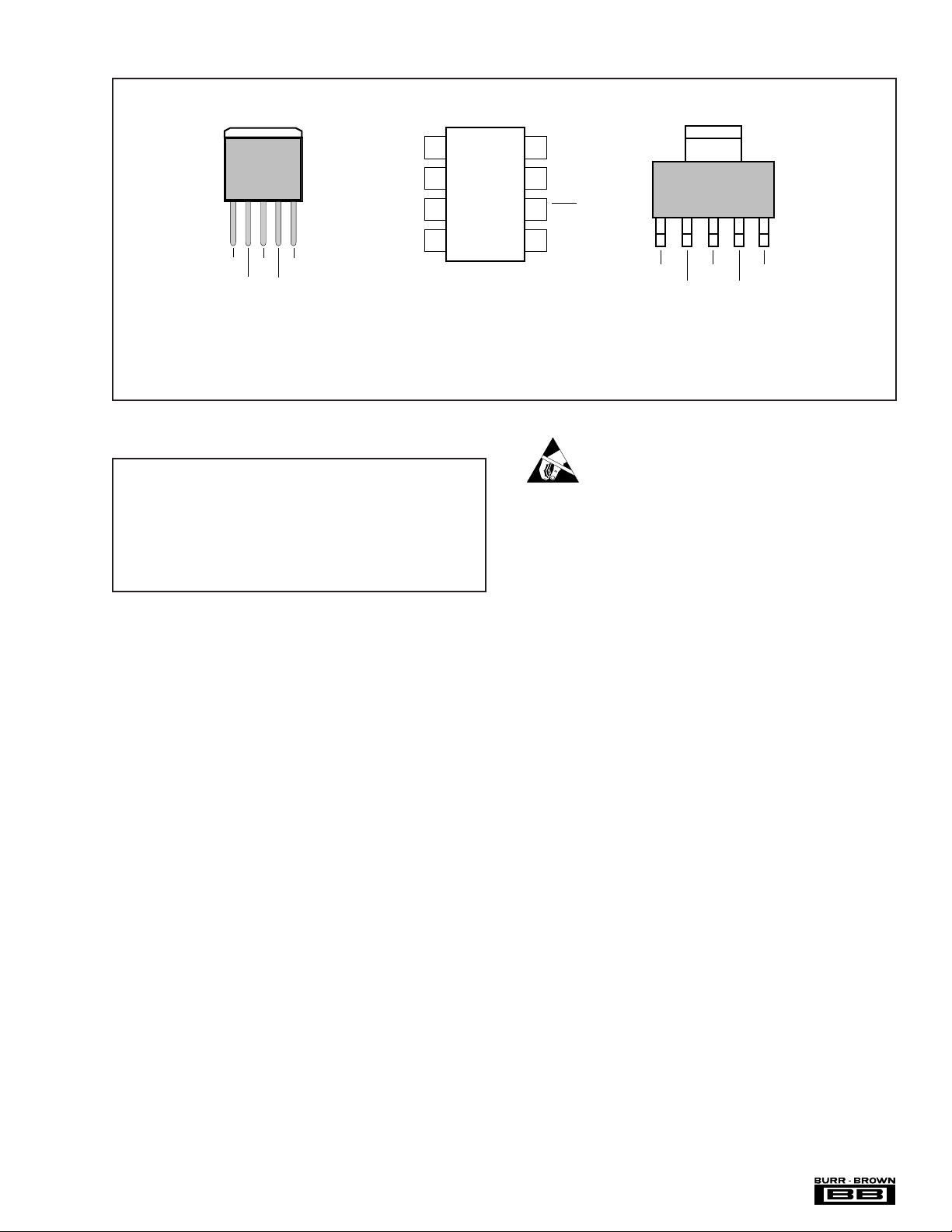
PIN CONFIGURATIONS
Top View
DDPAK-5
1234
V
GND
O
(1)
NR/Adjust
5
V
IN
Enable
Tab is GND
V
V
NR/Adjust
GND
OUT
OUT
SO-8
1
2
(1)
3
4
8
7
6
5
V
IN
V
IN
Error
Enable
SOT223-5
Tab is GND
12345
GNDV
IN
V
OUT
Enable
NR/Adjust
(1)
(FA Package)
NOTE: (1) For REG103A-A: voltage setting resistor pin.
All other models: noise reduction capacitor pin.
ABSOLUTE MAXIMUM RATINGS
Supply Input Voltage, VIN.......................................................–0.3V to 16V
Enable Input ............................................................................ –0.3V to V
Error Flag Output .....................................................................–0.3V to 6V
Error Flag Current ...............................................................................2mA
Output Short-Circuit Duration ......................................................Indefinite
Operating Temperature Range ....................................... –55°C to +125°C
Storage Temperature Range .......................................... –65°C to +150°C
Junction Temperature ..................................................... –55°C to +150°C
Lead Temperature
NOTE: (1) Stresses above these ratings may cause permanent damage.
Exposure to absolute maximum conditions for extended periods may degrade
device reliability.
(soldering, 3s, SO-8, SOT and DDPAK)
(1)
................ +240°C
(UA Package)
IN
(GA Package)
ELECTROSTATIC
DISCHARGE SENSITIVITY
This integrated circuit can be damaged by ESD. Burr-Brown
recommends that all integrated circuits be handled with
appropriate precautions. Failure to observe proper handling
and installation procedures can cause damage.
ESD damage can range from subtle performance degradation to complete device failure. Precision integrated circuits
may be more susceptible to damage because very small
parametric changes could cause the device not to meet its
published specifications.
The information provided herein is believed to be reliable; however, BURR-BROWN assumes no responsibility for inaccuracies or omissions. BURR-BROWN assumes
no responsibility for the use of this information, and all use of such information shall be entirely at the user's own risk. Prices and specifications are subject to change
without notice. No patent rights or licenses to any of the circuits described herein are implied or granted to any third party. BURR-BROWN does not authorize or warrant
any BURR-BROWN product for use in life support devices and/or systems.
3
REG103
®
Page 4

PACKAGE/ORDERING INFORMATION
PACKAGE SPECIFIED
PRODUCT PACKAGE NUMBER RANGE MARKING NUMBER
5V Output
REG103FA-5
(2)
DDPAK-5 325 –40°C to +85°C REG103FA-5.0 REG103FA-5 Rails
DRAWING TEMPERATURE PACKAGE ORDERING TRANSPORT
"""""REG103FA-5/500 Tape and Reel
REG103UA-5 SO-8 182 –40°C to +85°C REG103U50 REG103UA-5 Rails
"""""REG103UA-5/2K5 Tape and Reel
REG103GA-5
(2)
SOT223-5 364 –40°C to +85°C R103G50 REG103GA-5 Rails
"""""REG103GA-5/2K5 Tape and Reel
3.3V Output
REG103FA-3.3
(2)
DDPAK-5 325 –40°C to +85°C REG103FA-3.3 REG103FA-3.3 Rails
"""""REG103FA-3.3/500 Tape and Reel
REG103UA-3.3 SO-8 182 –40°C to +85°C REG103UA4 REG103UA-3.3 Rails
"""""REG103UA-3.3/2K5 Tape and Reel
REG103GA-3.3
(2)
SOT223-5 364 –40°C to +85°C R103G33 REG103GA-3.3 Rails
"""""REG103GA-3.3/2K5 Tape and Reel
3.0V Output
REG103FA-3
REG103UA-3
REG103GA-3
(2)
"""""REG103FA-3/500 Tape and Reel
(2)
"""""REG103UA-3/2K5 Tape and Reel
(2)
DDPAK-5 325 –40°C to +85°C REG103FA-3.0 REG103FA-3 Rails
SO-8 182 –40°C to +85°C REG103U30 REG103UA-3 Rails
SOT223-5 364 –40°C to +85°C R103G30 REG103GA-3 Rails
"""""REG103GA-3/2K5 Tape and Reel
2.7V Output
REG103FA-2.7
(2)
DDPAK-5 325 –40°C to +85°C REG103FA-2.7 REG103FA-2.7 Rails
"""""REG103FA-2.7/500 Tape and Reel
REG103UA-2.7 SO-8 182 –40°C to +85°C REG103U27 REG103UA-2.7 Rails
"""""REG103UA-2.7/2K5 Tape and Reel
REG103GA-2.7
(2)
SOT223-5 364 –40°C to +85°C R103G27 REG103GA-2.7 Rails
"""""REG103GA-2.7/2K5 Tape and Reel
2.5V Output
REG103FA-2.5
(2)
DDPAK-5 325 –40°C to +85°C REG103FA-2.5 REG103FA-2.5 Rails
"""""REG103FA-2.5/500 Tape and Reel
REG103UA-2.5 SO-8 182 –40°C to +85°C REG103U25 REG103UA-2.5 Rails
"""""REG103UA-2.5/2K5 Tape and Reel
REG103GA-2.5
(2)
SOT223-5 364 –40°C to +85°C R103G25 REG103GA-2.5 Rails
"""""REG103GA-2.5/2K5 Tape and Reel
Adjustable Output
REG103FA-A
(2)
DDPAK-5 325 –40°C to +85°C REG103FAA REG103FA-A Rails
"""""REG103FA-A/500 Tape and Reel
REG103UA-A SO-8 182 –40°C to +85°C REG103UA REG103UA-A Rails
"""""REG103UA-A/2K5 Tape and Reel
REG103GA-A
(2)
SOT223-5 364 –40°C to +85°C R103GA REG103GA-A Rails
"""""REG103GA-A/2K5 Tape and Reel
NOTES: (1) Models with a slash (/) are available only in Tape and Reel in the quantities indicated (e.g., /2K5 indicates 2500 devices per reel). Ordering 2500 pieces
of “REG103UA-5/2K5” will get a single 2500-piece Tape and Reel. (2) Scheduled availability June, 2000.
(1)
MEDIA
®
REG103
4
Page 5

TYPICAL PERFORMANCE CURVES
1000 200 300 400 500
180
160
140
120
100
80
60
40
20
0
DC Dropout Voltage (mV)
Output Current (mA)
DC DROPOUT VOLTAGE vs OUTPUT CURRENT
= –55°C
= +25°C
= +125°C
–75 –25–50 250 50 75 100 125
0.5
0.4
0.3
0.2
0.1
0
Output Voltage Change (%)
Temperature (°C)
LINE REGULATION vs TEMPERATURE
(V
IN
= V
OUT
+ 1V to VIN = 15V )
= 10mA
= 100mA
For all models, at TJ = +25°C and V
= 2V, unless otherwise noted.
ENABLE
OUTPUT VOLTAGE CHANGE vs I
(V
= V
IN
OUT
Refered to I
0.5
0
–0.5
–1.0
Output Voltage Change (%)
–1.5
= –55°C
= +25°C
= +125°C
1000 200 300 400 500
OUTPUT VOLTAGE CHANGE vs V
(Output Voltage % Change Refered
to V
0.5
IN
0
+ 1V, Output Voltage % Change
= 10mA at +25°C)
OUT
I
(mA)
OUT
= V
+ 1V at I
OUT
OUT
OUT
IN
= 10mA)
0.1
0.5
OUTPUT VOLTAGE vs TEMPERATURE
(Output Voltage % Change Referred to
I
= 10mA at +25°C)
OUT
–0.5
–1.0
Output Voltage Change (%)
–1.5
0246 108
Input Voltage Above V
DC DROPOUT VOLTAGE vs TEMPERATURE
160
120
80
40
DC Dropout Voltage (mV)
0
–75 –25–50 250 50 75 100 125
Temperature (°C)
OUT
= 10mA
= 100mA
= 500mA
= 10mA
= 100mA
= 500mA
0
–0.5
–1
Output Voltage Change (%)
–1.5
–75 –25–50 250 50 75 100 125
5
= 10mA
= 100mA
= 500mA
Temperature (°C)
®
REG103
Page 6

TYPICAL PERFORMANCE CURVES (Cont.)
For all models, at TJ = +25°C and V
= 2V, unless otherwise noted.
ENABLE
500mA
10mA
REG103-3.3
V
IN
200mV/div
200mV/div
REG103-Adj.
V
OUT
200mV/div
LOAD TRANSIENT RESPONSE
= 4.3V
C
= 0
OUT
C
= 10µF
OUT
10µs/div
LOAD TRANSIENT RESPONSE
= 3.3V, V
= 4.3V, C
IN
= 0.01µF
FB
LINE TRANSIENT RESPONSE
REG103-3.3
C
= 0
C
OUT
OUT
= 10µF
V
OUT
V
OUT
50mV/div
Load = 100mA
V
OUT
V
OUT
50mV/div
I
OUT
6V
V
IN
5V
50µs/div
LINE TRANSIENT RESPONSE
REG103-Adj.
= 3.3V, C
V
C
= 0
OUT
V
OUT
OUT
50mV/div
= 0.01µF, I
FB
= 100mA
OUT
C
= 0
OUT
V
OUT
C
OUT
200mV/div
500mA
10mA
10µs/div
LOAD REGULATION vs TEMPERATURE
0.5
IN
OUT
+ 1V and 10mA < I
< 500mA)
OUT
(V
= V
0.4
0.3
0.2
0.1
Output Voltage Change (%)
0
–75 –25–50 250 50 10075 125
Temperature (°C)
= 10µF
V
I
OUT
OUT
C
OUT
50mV/div
6V
5V
50µs/div
OUTPUT NOISE DENSITY
10
1
0.1
Noise Density (µV/√Hz)
CNR = 0
= 0
C
OUT
C
= 0.01µF
NR
C
= 10µF
OUT
0.01
10 100 1000 10000 100,000
Frequency (Hz)
= 10µF
V
OUT
V
IN
®
REG103
6
Page 7

TYPICAL PERFORMANCE CURVES (Cont.)
–75 –50 –25 0 25 50 75 100 125
3
2.5
2
1.5
1
0.5
0
I
GND
(µA)
Temperature (°C)
GROUND PIN CURRENT, NOT ENABLED
vs TEMPERATURE
V
ENABLE
= 0V
–20–40 0 40 80 120–60 20 60 100 140
0.28
0.26
0.24
0.22
0.20
0.18
0.16
0.14
Adjust Pin Current (µA)
Temperature (°C)
I
ADJUST
vs TEMPERATURE
REG103-A
For all models, at TJ = +25°C and V
= 2V, unless otherwise noted.
ENABLE
1.2
GROUND PIN CURRENT vs TEMPERATURE
1.1
1
0.9
(mA)
0.8
GND
I
0.7
0.6
0.5
0.4
–75 –25–50 250 50 75 100 125
Temperature (°C)
1.2
GROUND PIN CURRENT vs I
OUT
1.1
1
0.9
(mA)
0.8
GND
I
0.7
0.6
0.5
0.4
1 10 100 1000
I
(mA)
OUT
= 10mA
= 100mA
= 500mA
730
CURRENT LIMIT vs TEMPERATURE
720
710
700
690
680
670
660
Current Limit (mA)
650
640
630
–75 –50 –25 0 25 50 75 100 125
Temperature (°C)
70
RIPPLE REJECTION vs FREQUENCY
60
50
C
= 10µF
OUT
40
C
Ripple Rejection (dB)
V
= V
OUT
OUT-NOMINAL
V
= 1V
OUT
• 0.90
30
20
10 100 1000 10000 100000
OUT
= 0
Frequency (Hz)
®
7
REG103
Page 8

TYPICAL PERFORMANCE CURVES (Cont.)
For all models, at TJ = +25°C and V
= 2V, unless otherwise noted.
ENABLE
75
RIPPLE REJECTION vs I
70
V
= 3Vp-p, f = 120Hz
RIPPLE
OUT
65
60
55
50
Ripple Rejection (dB)
45
40
0 100 200 300 400 500
Load Current (mA)
OUTPUT DISABLE TIME
C
= 0
OUT
1V/div
2V
0
10µs/div
V
OUT
V
ENABLE
SOFT START
1V/div
2V
0
250µs/div
45
OUTPUT VOLTAGE DRIFT HISTOGRAM
40
35
30
25
20
15
Percent of Units (%)
10
5
0
40 45 50 55 60 65 70 75 80 85 90
V
Drift (ppm/°C)
OUT
V
OUT
V
ENABLE
®
REG103
60
OUTPUT VOLTAGE ACCURACY HISTOGRAM
50
40
30
20
Percent of Units (%)
10
0
–1 –0.8 –0.6 –0.4 –0.2 0 0.2 0.4 0.6 0.8 1
Error (%)
8
Page 9

BASIC OPERATION
The REG103 series is a family of LDO (Low Drop-Out)
linear regulators. The family includes five fixed output
versions (2.5V to 5.0V) and an adjustable output version. An
internal DMOS power device provides low dropout regulation with near constant ground pin current (largely independent of load and drop-out conditions) and very fast line and
load transient response. All versions include internal current
limit and thermal shutdown circuitry.
Figure 1 shows the basic circuit connections for the fixed
voltage models. Figure 2 gives the connections for the
adjustable output version (REG103A) and example resistor
values for some commonly used output voltages. Values for
other voltages can be calculated from the equation shown in
Figure 2. The SO-8 package provides two pins each for V
and V
adjacent to the device.
. Both sets of pins MUST be used and connected
OUT
None of the versions require an output capacitor for regulator stability. The REG103 will accept any output capacitor
type less than 1µF. For capacitance values larger than 1µF
the effective ESR should be greater than 0.1Ω. This minimum ESR value includes parasitics such as printed circuit
board traces, solder joints, and sockets. A minimum 0.1µF
low ESR capacitor connected to the input supply voltage is
recommended.
INTERNAL CURRENT LIMIT
The REG103 internal current limit has a typical value of
700mA. A fold-back feature limits the short-circuit current
to a typical short-circuit value of 40mA. This circuit will
protect the regulator from damage under all load conditions.
IN
A curve of V
3.5
3
2.5
OUT
versus I
is given in Figure 3.
OUT
REG103
Error
C
NR
0.01µF
Optional
V
OUT
C
OUT
Enable
V
IN
0.1µF
In Out
Gnd NR
FIGURE 1. Fixed Voltage Nominal Circuit for REG103.
ErrorEnable
8
V
IN
0.1µF
Pin numbers for SO-8 package.
7
V
OUT
To reduce current through divider, increase resistor
values (see table at right).
As the impedance of the resistor divider increases,
I
(~200nA) may introduce an error.
ADJ
C
improves noise and transient response.
FB
REG103
= (1 + R1/R2) • 1.295V
65
1
2
I
3
4
Gnd
ADJ
R
Adj
R
1
2
C
FB
0.01µF
2
1.5
Output Voltage (V)
1
0.5
0
0 100 200 300 400 500 600 700 800
Output Current (mA)
FIGURE 3. Foldback Current Limit of the REG103-3.3 at
25°C.
EXAMPLE RESISTOR VALUES
(V) R1 (Ω)
V
OUT
1.295 Short Open
2.5 12.1k 13k
3 16.9k 13k
3.3 20k 13k
5 37.4k 13k
NOTE: (1) Resistors are standard 1% values.
(1)
1.21k 1.3k
1.69k 1.3k
2.0k 1.3k
3.74k 1.3k
R2 (Ω)
(1)
C
OUT
Optional
Load
V
OUT
FIGURE 2. Adjustable Voltage Circuit for REG103A.
®
9
REG103
Page 10

REG103
Error
+5V
10kΩ
Pull-up
3 ENABLE
SO-8 Package
Only
6
Open
Drain
µP
ENABLE
The Enable pin allows the regulator to be turned on and off.
This pin is active high and compatible with standard TTLCMOS levels. Inputs below 0.5V (max) turn the regulator
off and all circuitry is disabled. Under this condition ground
pin current drops to approximately 0.5µA.
When not used, the enable pin may be connected to VIN.
Internal to the part, the enable pin is connected to an input
resistor-zener diode circuit, as shown in Figure 4, creating a
nonlinear input impedance. The Enable Pin Current versus
Applied Voltage relationship is shown in Figure 5. When the
enable pin is connected to VIN greater than 10V, a series
resistor may be used to limit the current.
ENABLE
175kΩ
V
= 10V
Z
FIGURE 6. ERROR Pin Typical Fault Monitoring Circuit.
OUTPUT NOISE
A precision band-gap reference is used for the internal
reference voltage, V
, for the REG103. This reference is
REF
the dominant noise source within the REG103. It generates
approximately 45µVrms in the 10Hz to 100kHz bandwidth
at the reference output. The regulator control loop gains up
the reference noise, so that the noise voltage of the regulator
is approximately given by:
FIGURE 4. ENABLE Pin Equivalent Input Circuit.
100
10
1
0.1
Enable Current (µA)
0.01
0.001
0 2 4 6 8 10 12 14 16
Enable Voltage
FIGURE 5. Enable Pin Current versus Applied Voltage.
ERROR FLAG
The error indication pin, only available on the SO-8 package
version, provides a fault indication out of regulation condition. During a fault condition, error is pulled low by an open
drain output device. The pin voltage, in the fault state, is
typically less than 0.2V at 500µA.
A fault condition is indicated when the output voltage differs
(either above or below) from the specified value by approximately 10%. Figure 6 shows a typical fault monitoring
application.
®
REG103
V Vrms
=µ
N
Since the value of V
RR
+
12
R
2
is 1.295V, this relationship reduces to:
REF
Vrms
V
N OUT
µ
=
V
Vrms
=µ •45
45
V
•35
V
OUT
V
REF
Connecting a capacitor, CNR, from the Noise Reduction
(NR) pin to ground, can reduce the output noise voltage.
Adding CNR (see Figure 7) forms a low-pass filter for the
voltage reference. For CNR= 10nF, the total noise in the
10Hz to 100kHz bandwidth is reduced by approximately
a factor of 3.5. This noise reduction effect is shown in
Figure 8.
The REG103 adjustable version does not have the noisereduction pin available, however, the adjust pin is the summing junction of the error amplifier. A capacitor, CFB,
connected from the output to the adjust pin will reduce both
the output noise and the peak error from a load transient.
See Figure 9 for improved output noise performance for two
capacitor combinations.
The REG103 utilizes an internal charge pump to develop an
internal supply voltage sufficient to drive the gate of the
DMOS pass element above VIN. The charge-pump switching noise (nominal switching frequency = 2MHz) is not
measurable at the output of the regulator.
DROP-OUT VOLTAGE
The REG103 uses an N-channel DMOS as the “pass”
element. When the input voltage is within a few hundred
millivolts of the output voltage, the DMOS device behaves
like a resistor. Therefore, for low values of VIN to V
10
OUT
, the
Page 11

250
200
150
100
50
0
Drop Out Voltage (mV)
0 100 200 300 400 500
I
OUT
(mA)
REG103 –3.3 at 25°C
DC
Transient
V
IN
NR
(fixed output
versions only)
C
NR
(optional)
Enable
FIGURE 7. Block Diagram.
45
V
REF
(1.295V)
Error
Low Noise
Charge Pump
Over Current
Over Temp
Protection
10.0
DMOS
Output
REG103
V
OUT
R
1
Adj
(Adjustable
R
Versions)
2
NOTE: R1 and R2 are internal
on fixed output versions.
35
10Hz - 100kHz)
RMS
Output Noise Voltage
(µV
25
0.001 0.01 0.1 1
FIGURE 8. Output Noise versus Noise Reduction Capacitor.
regulator’s input-to-output resistance is the RdsON of the
DMOS pass element (typically 230mΩ). For static (DC)
loads, the REG103 will typically maintain regulation down
to VIN to V
voltage drop of 115mV at full rated output
OUT
current. In Figure 10, the bottom line (DC dropout) shows
the minimum VIN to V
OUT
drop-out under DC load conditions.
For large step changes in load current, the REG103 requires
a larger voltage drop across it to avoid degraded transient
response. The boundary of this “transient drop-out” region is
shown as the top line in Figure 10. Values of VIN to V
voltage drop above this line insure normal transient response.
In the transient dropout region between “DC” and “Transient”, transient response recovery time increases. The time
required to recover from a load transient is a function of both
the magnitude and rate of the step change in load current and
C
= 0
OUT
= 10µF
C
OUT
CNR (µF)
voltage drop required to prevent
OUT
1.0
nV/√Hz
C
= 0, CFB = 0
OUT
C
= 0, CFB = 0.01µF
OUT
C
= 10µF, CFB = 0.01µF
0.1
OUT
10010 1000 10000 100000
Frequency
FIGURE 9. Output Noise Density on Adjustable Versions.
FIGURE 10. Transient and DC Dropout.
11
REG103
®
Page 12

the available “headroom” VIN to V
voltage drop. Under
OUT
worst-case conditions (full-scale load change with VIN to
V
voltage drop close to DC dropout levels), the REG103
OUT
can take several hundred microseconds to re-enter the specified window of regulation.
TRANSIENT RESPONSE
The REG103 response to transient line and load conditions
improves at lower output voltages. The addition of a capacitor (nominal value 10nF) from the output pin to ground may
improve the transient response. In the adjustable version, the
addition of a capacitor, CFB (nominal value 10nF), from the
output to the adjust pin will also improve the transient
response.
heat from the device. In those examples where there is
copper on both sides of the PCB, no connection has been
provided between the two sides. The addition of plated
through holes will improve the heat sink effectiveness.
Power dissipation depends on input voltage and load conditions. Power dissipation is equal to the product of the
average output current times the voltage across the output
element, VIN to V
PVV I
voltage drop.
OUT
=•(– )
D IN OUT OUT AVG
()
Power dissipation can be minimized by using the lowest
possible input voltage necessary to assure the required
output voltage.
THERMAL PROTECTION
Power dissipated within the REG103 will cause the junction
temperature to rise. The REG103 has thermal shutdown
circuitry that protects the regulator from damage. The thermal protection circuitry disables the output when the junction temperature reaches approximately 150°C, allowing the
device to cool. When the junction temperature cools to
approximately 130°C, the output circuitry is again enabled.
Depending on various conditions, the thermal protection
circuit may cycle on and off. This limits the dissipation of
the regulator, but may have an undesirable effect on the load.
Any tendency to activate the thermal protection circuit
indicates excessive power dissipation or an inadequate heat
sink. For reliable operation, junction temperature should be
limited to 125°C, maximum. To estimate the margin of
safety in a complete design (including heat sink), increase
the ambient temperature until the thermal protection is
triggered. Use worst-case loads and signal conditions. For
good reliability, thermal protection should trigger more than
35°C above the maximum expected ambient condition of
your application. This produces a worst-case junction temperature of 125°C at the highest expected ambient temperature and worst-case load.
The internal protection circuitry of the REG103 has been
designed to protect against overload conditions. It was not
intended to replace proper heat sinking. Continuously running the REG103 into thermal shutdown will degrade reliability.
POWER DISSIPATION
The REG103 is available in three different package configurations. The ability to remove heat from the die is different
for each package type and, therefore, presents different
considerations in the printed circuit-board layout. The PCB
area around the device that is free of other components
moves the heat from the device to the ambient air. While it
is difficult-to-impossible to quantify all of the variables in a
thermal design of this type, performance data for several
configurations are shown in Figure 11. In all cases the PCB
copper area is bare copper, free of solder resist mask, and not
solder plated. All examples are for 1-ounce copper. Using
heavier copper will increase the effectiveness in moving the
®
REG103
REGULATOR MOUNTING
The tab of both packages is electrically connected to ground.
For best thermal performance, the tab of the DDPAK surface-mount version should be soldered directly to a circuitboard copper area. Increasing the copper area improves heat
dissipation. Figure 12 shows typical thermal resistance from
junction to ambient as a function of the copper area for the
DDPAK.
Although the tabs of the DDPAK and the SOT-223 are
electrically ground, they are not intended to carry any
current. The copper pad that acts as a heat sink should be
isolated from the rest of the circuit to prevent current flow
through the device from the tab to the ground pin. Solder pad
footprint recommendations for the various REG103 devices
are presented in Application Bulletin “Solder Pad Recommendations for Surface-Mount Devices” (AB-132), available from the Burr-Brown web site (www.burr-brown.com).
6
5
4
3
2
Power Dissipation (Watts)
1
0
0 25 50 75 100 150125
Ambient Temperature (°C)
CONDITION PACKAGE PCB AREA THETA J-A
1 DDPAK 4in
2 SOT-223 4in
3 DDPAK None 65°C/W
4 SOT-223 0.5in
5 SO-8 None 150°C/W
2
Top Side Only 27°C/W
2
Top Side Only 53°C/W
2
Top Side Only 110°C/W
CONDITIONS
FIGURE 11. Maximum Power Dissipation versus Ambient
Temperature for the Various Packages and
PCB Heat Sink Configurations.
12
#1
#2
#3
#4
#5
Page 13

THERMAL RESISTANCE vs PCB COPPER AREA
50
40
(°C/W)
JA
30
20
10
Thermal Resistance, θ
0
012345
Copper Area (inches
REG103
Surface Mount Package
1 oz. copper
2
)
FIGURE 12. Thermal Resistance versus PCB Area for the Five Lead DDPAK.
Circuit Board Copper Area
REG103
DDPAK Surface Mount Package
180
160
140
(°C/W)
JA
120
θ
100
Thermal Resistance,
THERMAL RESISTANCE vs PCB COPPER AREA
REG103
Surface Mount Package
1 oz. copper
80
60
40
20
0
012345
Copper Area (inches
2
)
FIGURE 13. Thermal Resistance versus PCB Area for the Five Lead SOT-223.
Circuit Board Copper Area
REG103
SOT-223 Surface Mount Package
13
®
REG103
 Loading...