

Page 1

INTEGRATED CIRCUITS
HTRC110
Hitag Reader Chip
Product Specification (Rev. 1.1)
December 1997
Page 2

Philips Semiconductors Product Specification
Hitag Reader Chip HTRC110
CONTENTS
1 FEATURES
2 GENERAL DESCRIPTION
3 ORDERING INFORMATION
4 BLOCK DIAGRAM
5 KEY DATA
6 PINNING INFORMATION
6.1 Pinning Diagram
6.2 Pin Description
7 MINIMUM APPLICATI ON CIRCUI TRY
8 FUNCTIONAL DESCRIPT ION
8.1 Power Supply
8.2 Antenna Drivers, Data Input
8.3 Diagnosis
8.4 Oscillator / Programmable Divider / Clock
8.5 Adaptive Sampling Time Demodulator
8.6 Idle and Power-down Mode
8.7 Serial Interface
8.7.1 Glitch Filter for Increased Noise/Interference Imm unity
9 COMMANDS
9.1 READ_TAG
9.2 WRITE_TAG_N
9.3 WRITE_TAG
9.4 READ_PHASE
9.5 SET_SAMPLING_TI ME
9.6 GET_SAMPLING_TIME
9.7 SET_CONFIG_PAG E
9.8 GET_CONFIG_PAGE
10 ABSOLUTE MAXIMUM RATINGS
11 DC CHARACTERISTICS
12 AC CHARACTERISTICS
13 PACKAGE
14 DEFINITIONS
15 LIFE SUPPORT APPLICATIONS
Rev. 1.1 2
Page 3

Philips Semiconductors Product Specification
Hitag Reader Chip HTRC110
1 FEATURES
Combines all analogue RFID reader hardware in a single
chip
· Optimized for HITAG transponder family
· Robust antenna coil power driver stage with modulator
· High performance adaptive sampling time AM/PM
demodulator (patent pending)
· Read and write function
· On-chip clock oscillator
· Antenna rupture and short circuit detection
· Low power consumption
· Very low power stand-by mode
· Low external component count
· Small package (SO14)
2 GENERAL DESCRIPTION
The Hitag Reader Chip HTRC110 is intended for use
with transponders which are based on the HITAG silicon (HT1ICS30 02x or HT2ICS20 02x). (E.g. the
HITAG 2 stick HT2DC20 S20 may be operated with the
use of the Reader Chip). In addition the IC supports
other 125kHz transponder types using amplitude modulation for the write operation and AM/PM for the read
operation. The receiver parameters (gain factors, filter
cutoff frequencies) can be optimized to system and
transponder requirements. The HTRC110 is designed
for easy integration into RF-identification readers.
State-of-the-art technology a llows alm ost c omplete integration of the necessary building blocks. A powerful
antenna driver/modulator together with a low-noise
adaptive sampling time demodulator, programmable filters/amplifier and digitizer build the complete transceiver unit, required to design high-performance
readers. A three-pin microcontroller interface is
employed for programming the HTRC110 as well as for
the bidirectional communication with the transponders.
The three-wire interface can be changed into a
two-wire interface by connecting the data input and the
data output.
Tolerance dependent zero amplitude modulation
caused severe problems in envelope detector systems,
resulting in the need of very low tolerance reader antennas. These problems are solved by the new Adaptive
Sampling Time technique (AST).
3 ORDERING INFORMATION
TYPE NAME DESCRIPTION ORDERING NUMBER
HTRC110 01T/02EE Hitag Reader IC, Tube 9352 600 91112
HTRC110 01T/03EE Hitag Reader IC, Reel 9352 600 92118
Rev. 1.1 3
Page 4
Philips Semiconductors Product Specification
Hitag Reader Chip HTRC110
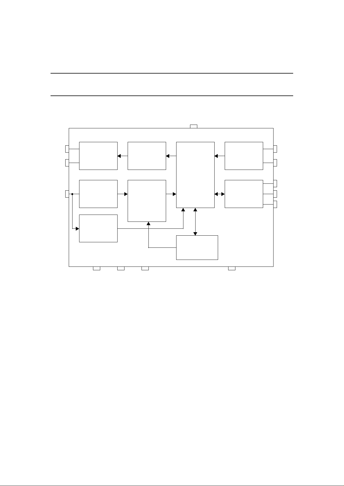
4 BLOCK DIAGRAM
VDD
TX1
TX2
RX
5 KEY DATA
Antenna Drivers Modulator
Synchron
Demodulator
Phase
Measurement
QGND CEXT
Bandpass Filter
Amplifier
Dynamic Control
Digitizer
VSS
Fig.1 Block diagram Hitag Reader Chip HTRC110
Control
Unit
Control Register
Oscillator
Serial Interface
MODE
XTAL1
XTAL2
DIN
DOUT
SCLK
Supply VDD 5 V ±10%
Clock/Osc. frequency 4,8,12,16 MHz programmable
(antenna carrier frequency 125 kHz)
Antenna driver current 200 mAp continuous
Serial interface CMOS compatible
Package SO14
Operation temperature range -40°C to +85°C
Rev. 1.1 4
Page 5

Philips Semiconductors Product Specification
Hitag Reader Chip HTRC110
6 PINNING INFORMATION
6.1 Pinning Diagram
6.2 Pin Description
Number Symbol Description
1 VSS GND, negative supply input
2 TX2 Coil driver output
3 VDD Stabilized 5 V supply input
4 TX1 Coil driver output
5 MODE To enable filtering of SCLK and DIN (for active antenna applications)
6 XTAL1 Oscillator interface, input
7 XTAL2 Oscillator interface, output
8 SCLK Microcontroller interface: serial clock input
9 DIN Microcontroller interface: serial data in
10 DOUT Microcontroller interface: serial data out
11 n.c. Not connected
12 CEXT High pass filter coupling
13 QGND Analog ground bias
14 RX Demodulator input
Rev. 1.1 5
Page 6
Philips Semiconductors Product Specification
Hitag Reader Chip HTRC110
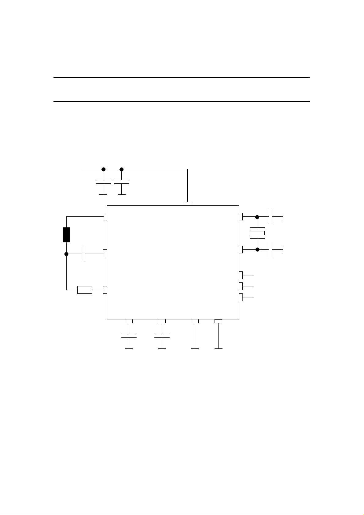
7 MINIMUM APPLICATIO N CIRCUI TRY
The following figure shows a minimal application circuitry for the HTRC110. The reader coil L
together with the
a
capacitor Ca forms a series resonant LC circuit (f = 125 kHz). The high voltages in the LC circuit are divided to safe
operating levels by R
and the chip internal resistor R
v
behind the RX-pin. The two capacitors connected to
dem_in
XTAL1 and XTAL2 shall be the recommended values and types from th e crystal’s dat a sheet. Alte rnatively to a crys tal a ceramic resonator can be used or an external clock source can be connected to XTAL1.
VDD
+
L
10µF
a
TX1
C
a
TX2
100nF
VDD
XTAL1
XTAL2
DIN
R
v
RX
DOUT
SCLK
TO
MICROPROCESSOR
QGND
CEXT VSS
MODE
100nF100nF
Fig.2 Minimum application circuitry
Rev. 1.1 6
Page 7

Philips Semiconductors Product Specification
Hitag Reader Chip HTRC110
8 FUNCTIONAL DESCRIPTION
8.1 Power Supply
The HTRC110 works with an external 5V±10% power
supply at VDD. The maximum DC-current is
10mA+Î
*2/π = 137mA. For optimum performance, the
ant
power supply connection should be bypassed t o ground
with a 100nF capacitor close to the IC.
8.2 Antenna Drivers, Data Input
The drivers deliver a square shaped voltage to the ser ies
resonant antenna circuit. Due to the full bridge
configuration of the drivers this voltage U
approximately 10V (peak-peak) corresponding to Û
is
drv
pp
=5V.
drv
The current flowing through the antenna is sine shaped.
It´s amplitude is approximately:
ˆ
U
4
ˆ
I
ant
drv
-----------
-- -
I
R
π
ant
ant
rms
ˆ
I
ant
=⇔=
--------2
8.3 Diagnosis
In order to detect an antenna short or open condition th e
antenna tap voltage is monitored. An antenna fail condition
is reported in the status bit ANTFAIL (see Table 14), if the
antenna tap voltage does not go more negative than the
diagnosis level DLEV (see Table 16). This condition is
checked for every coil driver cycle.
8.4 Oscillator / Programmable Divid er / Clock
The crystal oscillator at X TAL1/2 works with either crystal or ceramic resonators. It delivers the input clock frequency of 4,8,12 or 16 MHz. T he oscillator frequency is
divided by a programmable divider to obtain the carrier
frequency of 125 kHz (see Table 10).
Alternatively, an external clock signal (CMOS compatible) may be fed into the IC via XTAL1. For example, this
signal can be derived from the microcontroller clock.
8.5 Adaptive Sampling Time Demodulato r
The demodulator senses the absorption modulation
applied by a transponder when inserted into the field.
The signal is picked up at the antenna tap point between
and Ca. It is divided by Rv and the internal resistor
L
a
to a level below 8V (peak) with respect t o QGND
R
dem_in
at the RX-pin (see Fig.2). Internally the s ignal is filtered
with a second order low pass filter.
The antenna current and therefore the tap voltage is
modulated by the transponder in amplitude and/or
phase. This signal is fed into a synchronous demodulator
recovering the baseband signal. The amplification and
the bandpass filter edge frequencies of the demodulator
can be adapted to different transponders via settings in
the configuration pages.
The phase between the driver excitation signal and t he
antenna tap voltage depends on the antenna tuning.
With optimum tuning, the phase of the antenna tap voltage is 90 degrees off the antenna driver signal. Detuning
of the antenna resonant circ uit results in a change of this
phase relationship.
The HTRC110‘s built-in phase measurement unit allows
the measurement of this phase relationship with a reso lution of 360o/64=5.625o. This can be used to compute a
sampling time that compensates the mistuning of the
reader antenna. The phase measurement procedure can
be carried out
- either once before the first communication starts, if the
position of the transponder does not change with the
respect to the reader antenna
- or during the communication (after sending the write
pulses and before receiving the answer of the transponder), if the tag is moving.
Before the system is switched into WRITE_TAG-mode,
the demodulator has to be frozen. This is internally done
by clamping the input of the amplifier/filter unit to QGND.
Doing so avoids large transients in the amplifier and the
digitizer, which could affect settling times. In addition to
the clamping, there exist other means in the HTR C110
which allow further reduction of the settling times. All the
parts of the circuitry, which are associated with these
functions, are controlled by the FREEZE0, FREEZE1
and THRESET bits, which are located in configuration
page 2.
For more details concerning WRITE T iming, Demodulator Setting, Power Up Sequence, etc. please refer to t he
HTRC110 application note.
8.6 Idle and Power-down Mode
The HTRC110 can be switched into idle mode via settin g
the PD-bit and resetting the PD_MODE-bit. In this idle
mode, only the oscillator and a few other s ystem components are active.
It is also possible to switch the IC completely off. This is
achieved by the power-down mode (PD=1,
PD_MODE=1). Within this mode also the clock oscillator
is switched off. This reduces the supply current of the
HTRC110 to less than 20µA.
Rev. 1.1 7
Page 8
Philips Semiconductors Product Specification
Hitag Reader Chip HTRC110
8.7 Serial Interface
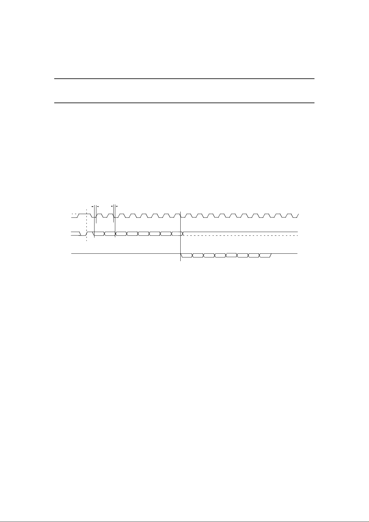
The communication between the HTRC110 and the microcontroller is done via a three wire digital interface. The interface is operated by the following signals:
SCLK Clock
DIN Data Input
DOUT Data Output
SCLK and DIN are realized as Schmitt-Trigger inputs. DOUT is an open drain output with internal pullup resistor.
Every communication between HTRC110 and microcontroller begins with an initialization of the serial interface. The
interface initialization condition is a low-to-high transition of the signal DIN while SCLK is high.
T
T
S
H
SCLK
DIN
DOUT
initialization
D7
D6
D4
D5
D3
D2 D1
D0
D2 D1
D7
D6
D5
D3
D4
D0
All commands are transmitted to the HTRC110 serial interface starting with Most Significant Bit (MSB). DIN and DOUT
are valid when SCLK is high.
8.7.1 Glitch Filter for Increased Noise/Interference Immunity
Connecting Pin 5 (MODE) to VDD enables digital filtering of the SCLK and the DIN input signals. This mode offers
improved immunity against glitches on these interface signals. It is intended to be used in the so called “Active Antenna
Applications” where the microcontroller and the reader communicate via long signal lines (e.g. 1 meter).
In other applications Pin 5 (MODE) has to be connected to GND.
Please refer to the HTRC110 application note for a detailed description of this feature.
Rev. 1.1 8
Page 9
Philips Semiconductors Product Specification
Hitag Reader Chip HTRC110
9 COMMANDS
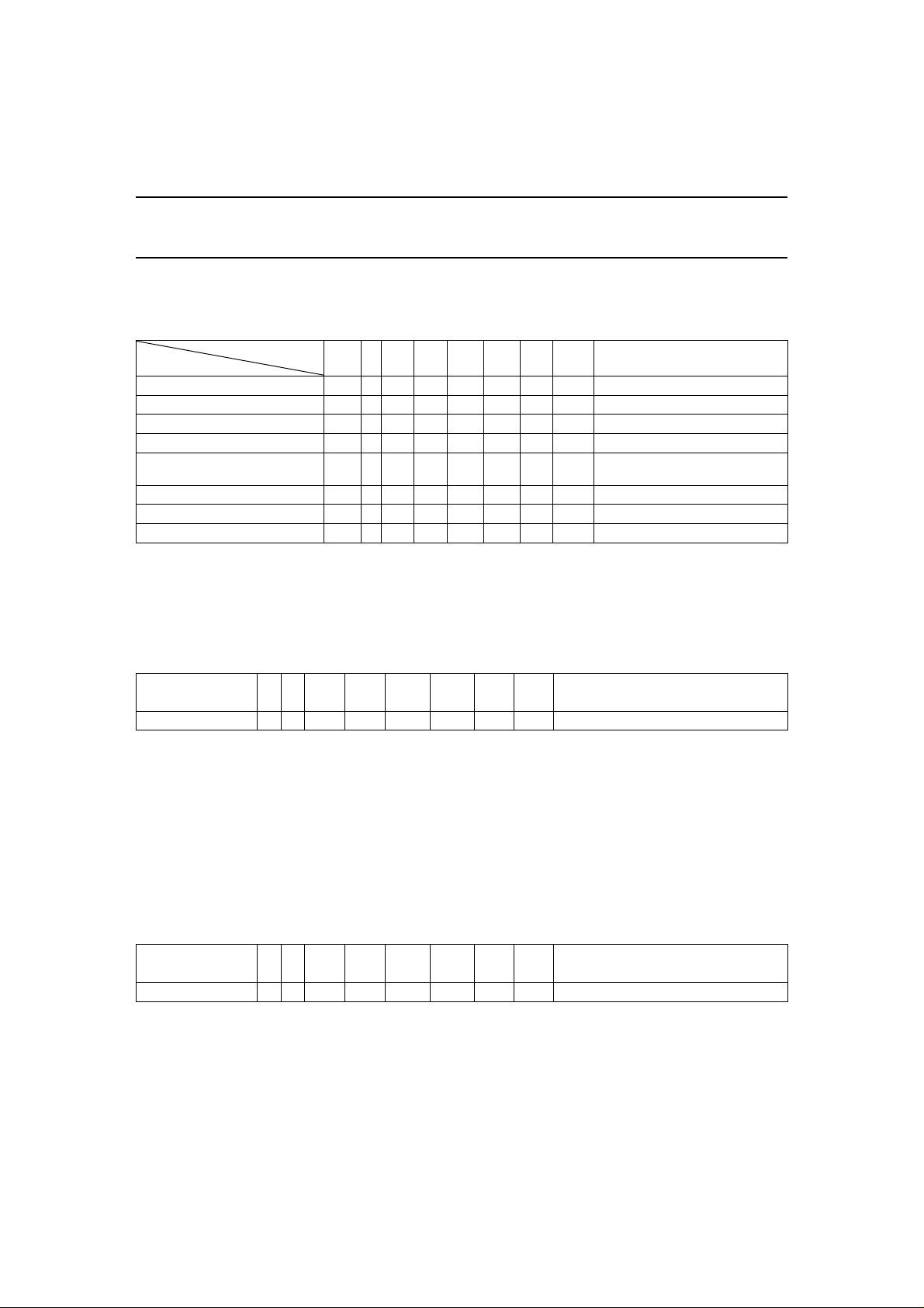
Table 1 depicts the HTRC110 command set summary.
Table 1:
Bit No. 7 6 5 4 3 2 1 0 Remark
Command Name MSB LSB
GET_SAMPLING_TIME
GET_CONFIG_PAGE
READ_PHASE 000 0 1 0 0 0
READ_TAG
WRITE_TAG_N 0 0 0 1 N3 N2 N1 N0
WRITE_TAG 110 - - - - -
SET_CONFIG_PAGE
SET_SAMPLING_T IME 1 0 D5 D4 D3 D2 D1 D0
9.1 READ_TAG
This command is used to read the demodulated bit stream from a transponder: After the assert ion of the three command bits the HTRC110 instantaneously switches to READ_TAG-mode and transmits the demodulated, filtered and
digitized data from the transponder. Data comes out and should be decoded by the microcontroller.
READ_TAG-mode is terminated by a low to high transition at SCLK.
Table 2:
000 0 0 0 1 0
000 0 0 1P1P0
111 - - - - -
0 1 P1 P0 D3 D2 D1 D0
8 bit resp. (0 0 D5-D0)
8 bit resp. (X3-X0 D3-D0)
8 bit resp. (0 0 D5 - D0)
READ_TAG-mode
WRITE_TAG-mode with pulse
width programming
WRITE_TAG-mode
4*4 config bits available
Bit No. 7 6 5 4 3 2 1 0 Remark
Command 1 1 1 - - - - - received data available at DOUT
9.2 WRITE_TAG_N
This command is used to write data to a transponder.
If N3-N0 are set to zero, the signal from DIN is transparently switched to the drivers. A high level at DIN corresponds
to antenna drivers switched off, a low level corresponds to antenna drivers switched on.
If any binary number between 1 and 1111 is loaded into N3- N0 the drivers are s witched off at the next positive transi-
tion of DIN. This stat e is held for a time interval equa l to N * T
requirements to the microcontroller and to the software implementation while providing an exact, selectable write
pulse timing. WRITE_TAG-mode is terminated immediat ely by a low to high transition at SCLK.
Table 3:
Bit No. 7 6 5 4 3 2 1 0 Remark
Command 0 0 0 1 N3 N2 N1 N0 no respons e
9.3 WRITE_TAG
This is the 3 bit short form of the previously described command WRITE_TAG_N. It allows to switch into
WRITE_TAG-mode with a minimum commun ication time.
Rev. 1.1 9
(T0=8µs). This method relaxes the timing res olution
0
Page 10

Philips Semiconductors Product Specification
Hitag Reader Chip HTRC110
The behaviour of the WRITE_TAG command is identical to WRITE_TAG_N with two exc eptions:
WRITE_TAG-mode is entered after asser tion of the 3rd com mand bit.
No N parameter is specified with this command; instead the N value which was programmed with the most recent
WRITE_TAG_N command is used. If no WRITE _TAG_N was issued so far, a default N=0 (transparent mode) will be
assumed.
Table 4:
Bit No. 7 6 5 4 3 2 1 0 Remark
Command 1 1 0 - - - - - no response
9.4 READ_PHASE
This command is used to read the antenna´s phase, which is measured at every carrier cycle.
The phase is coded binary in D5-D0.
Table 5:
Bit No. 7 6 5 4 3 2 1 0 Remark
Command 0 0 0 0 1 0 0 0
Response 0 0 D5 D4 D3 D2 D1 D0
9.5 SET_SAMPLING_TIME
This command specifies the demodulator sampling time t
Table 6:
Bit No. 7 6 5 4 3 2 1 0 Remark
Command 1 0 D5 D4 D3 D2 D1 D0 no response
9.6 GET_SAMPLING_TIME
This command is used to read back the sampling time t
coded binary in D5- D0.
Table 7:
Bit No. 7 6 5 4 3 2 1 0 Remark
Command 0 0 0 0 0 0 1 0
Response 0 0 D5 D4 D3 D2 D1 D0
Rev. 1.1 10
. The sampling time is coded binary in D5-D0.
s
set with SET_SAMPLING_TIME. The sampling time is
s
Page 11
Philips Semiconductors Product Specification
Hitag Reader Chip HTRC110
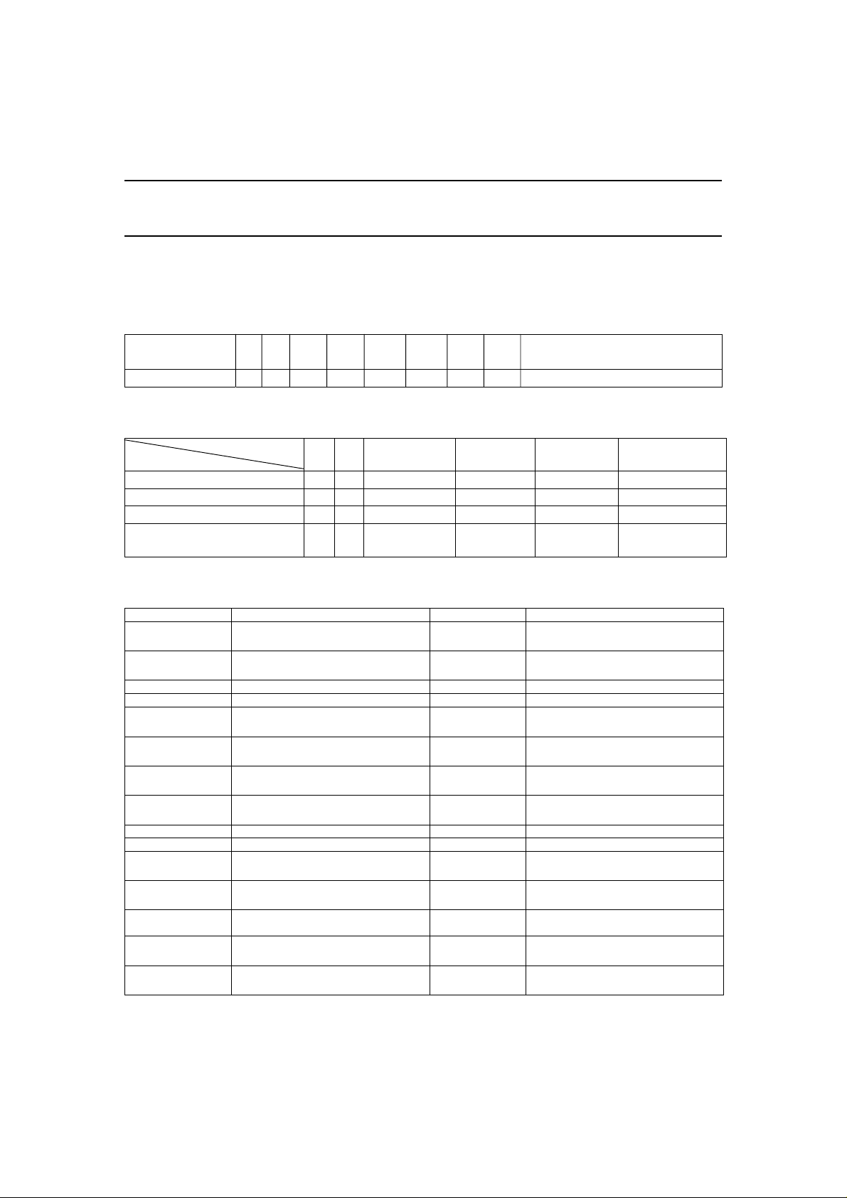
9.7 SET_CONFIG_PAGE
This command is used to set the amplifier and filter parameters (cutoff frequencies, gain factors) and the different
operation modes. P1 and P0 select one of four configuration pages.
Table 8:
Bit No. 7 6 5 4 3 2 1 0 Remark
Command 0 1 P1 P0 D3 D2 D1 D0 no response
Table 9:
Bit No. P1 P0 D3 D2 D1 D0
Command/Page No.
SET_CONFIG_PAGE 0
SET_CONFIG_PAGE 1 0 1 PD_MODE PD HYSTERESIS TXDIS
SET_CONFIG_PAGE 2
SET_CONFIG_PAGE 3 1 1 DISLP1 DISSMART-
0 0 GAIN1 GAIN0 FILTERH FILTERL
1 0 THRESET ACQAMP FREEZE1 FREEZE0
FSEL1 FSEL0
COMP
Table 10:
Bit name Description Initial condition
FILTERL main low pass cutoff frequency 0 0: fL = 3 kHz
1: fL = 6 kHz
FILTERH main high pass cutoff frequency 0 0: fH = 40 Hz
1: fH = 160 Hz
GAIN0 amplifier_0 gain factor 0 0: gain
GAIN1 amplifier_1 gain factor 1 0: gain
= 16; 1: gain0 = 32
0
= 6.22; 1: gain1 = 31.5
1
TXDIS disable coil driver 0 0: coil driver active
1: coil driver inactive
HYSTERESIS data comparator hyster esis 0 0: hysteresis OFF
1: hysteresis ON
PD power down mode enable 0 0: device active
1: device power down
PD_MODE select power down mode 0 0: idle mode
1: power down
FREEZE0 facility to achieve fast settl ing times 0 see table 11
FREEZE1 facility to achieve fast settl ing times 0 see table 11
ACQAMP store signal amplitude as reference
0 see status bit AMPCOMP
for later amplitude comparison
THRESET reset threshold generation of
0
digitizer
FSEL0 clock frequency select LSB 0 00: 4MHz, 01: 8MHz
FSEL1 clock frequency select MSB 0 10: 12MHz, 11: 16MHz
DISSMARTCOMP d isable smart comparat or 0 0: smart comparator = ON
1: smart comparator = OFF
DISLP1 d isable low pass 1 0 0: low pass = ON
1: low pass = OFF
Rev. 1.1 11
Page 12
Philips Semiconductors Product Specification
Hitag Reader Chip HTRC110
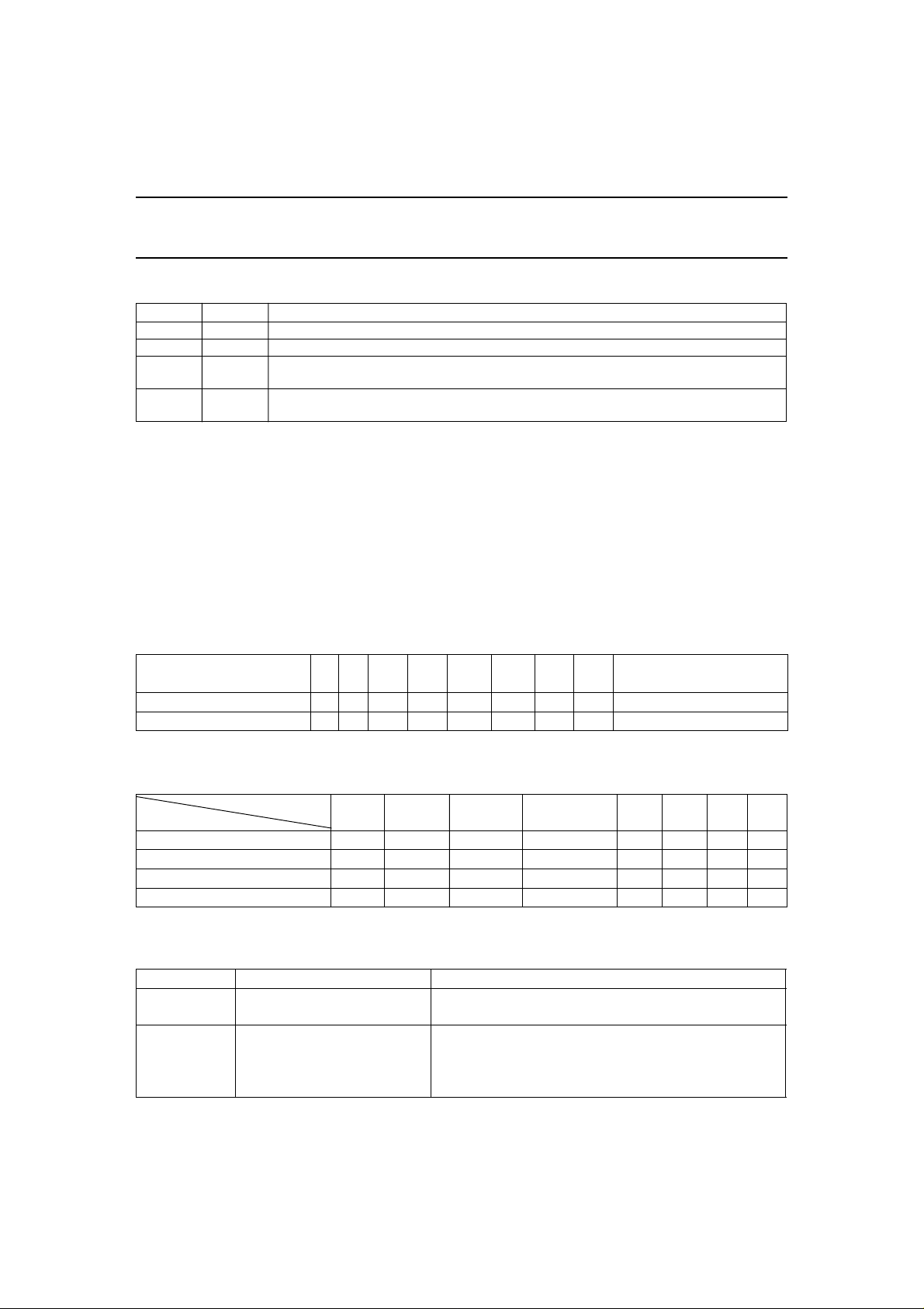
Table 11: Freeze Bit Descript ion
FREEZE1 FREEZE0 Meaning
0 0 normal operation
0 1 main low pass is frozen; main high pass is precharged to QGND
1 0 main low pass is frozen; time constant of main high pass is reduced by a factor of 16 for
FILTERH=0 and by a factor of 8 for FILTERH=1
1 1 time constant for main high pass is reduced by a factor of 16 for FILTERH=0 and by a factor
of 8 for FILTERH=1; second high pass is precharged
9.8 GET_CONFIG_PAGE
This command has three functions:
1. Reading back the configuration parameters set by SET_CONFI G_P AGE comm a nd
2. Reading back the transmit pulse width programmed with WRITE_TAG_N
3. Reading the system status information
P1 and P0 select one of four configuration pages. The response (X 3 X2 X1 X0 D3 D2 D1 D0) contains the content s of
the selected configuration page in its lower nibble. F or P=0 or P=1 the higher nibble reflects the current setting of N
(the transmit pulse width). For P=2 or P=3 the system status information is returned in the higher nibble.
Table 12:
Bit No. 7 6 5 4 3 2 1 0 Remark
Command 0 0 0 0 0 1 P1 P0
Response X3 X2 X1 X0 D3 D2 D1 D0
Table 13:
Bit No. 7 6 5 4 3 2 1 0
Command/Page No.
GET_CONFIG_PAGE 0
GET_CONFIG_PAGE 1 N3 N2 N1 N0 D3 D2 D1 D0
GET_CONFIG_PAGE 2
GET_CONFIG_PAGE 3 0 (RFU) 0 (RFU) AMPCOMP ANTFAIL D3 D2 D1 D0
Table 14: Status Bit Description
Bit name Meaning
ANTFAIL antenna failure 0: antenna ok
AMPCOMP amplitude comparison result W hen ACQ AMP is set , the actual amp litude of the data signal
N3 N2 N1 N0 D3 D2 D1 D0
0 (RFU) 0 (RFU) AMPCOMP ANTFAIL D3 D2 D1 D0
1: antenna failure
is stored as reference. After resetting ACQAMP status bit AMPCOMP is set when the actual data signal amplitude is higher
than the stored reference.
Rev. 1.1 12
Page 13

Philips Semiconductors Product Specification
Hitag Reader Chip HTRC110
10 ABSOLUT E MAX IMUM RAT ING S
Table 15 lists the limiting values. Stress above one or more of the limiting values may cause perm anent damage to
the device. These are stress ratings only and operation of the device at these or at any other conditions above those
given in the characteristics sections of this spec ification is not implied. Exposure to limiting values for extende d periods may affect device reliability.
Table 15:
Parameter Symbol Min. Max. Unit
Voltage at any pin except RX -0.3 +6.5 V
Voltage at any pin except RX -0.3 VDD+0.3 V
Voltage at RX pin -10 +12 V
Maximum junction temperature T
Storage temperature range T
store
j
-65 +125 °C
140 °C
Rev. 1.1 13
Page 14

Philips Semiconductors Product Specification
Hitag Reader Chip HTRC110
11 DC CHARACTERISTICS
, T
Table 16 lists the DC characteristics. All voltages are measured to V
= -40°C to +85°C.
ss
amb
Table 16:
Parameter Conditions Symbol Min. Typ. Max. Unit
Supply
Supply voltage VDD 4.5 5.0 5.5 V
Operating supply current VDD=5.5V, I
Idle current
(1)
VDD=5.5V I
TX1=ITX2
=0 I
Power down current VDD=5.5V I
On
id
pd
410mA
0.2 0.4 mA
720µA
Drivers (TX1, TX2)
Output peak-current permanent I
Output peak-current 1:4 On/off-ratio
<400ms
t
on
ant
I
antPulse
200 mA
400 mA
Output resistance both drivers together 2.5 7 Ω
Demodulator Input
Voltage range U
with respect to
RX
-8 8 V
QGND
QGND Potential 0.35 VDD 0.42 VDD 0.5 VDD V
Impedance R
dem_in
17 25 33 kΩ
Diagnosis Level (DLEV)
with respect to
U
RX
DLEV -1.5 -1.15 -0.8 V
QGND, VDD=5V
Digital Inputs
Data input high voltage V
Data input low voltage V
IH
IL
0.7 VDD VDD+0.3 V V
- 0.3 V 0.3 VDD V
Digital Outputs
Output low I
Output drive capability V
= +1mA V
OL max
≤ 0.4V 1 mA
OL
OL
0.4 V
p
p
1. Power consumption of external quartz or any other external component is not included
Rev. 1.1 14
Page 15

Philips Semiconductors Product Specification
Hitag Reader Chip HTRC110
12 AC CHARACTERISTI CS
Table 17 lists the AC characteristics. T
= -40°C to +85°C.
amb
Table 17:
Parameter Conditions Symb ol Min. Typ. Max. Unit
XTAL Oscillator (XTAL1/XTAL2)
Frequency range depending on FSEL f
osc
416MHz
Start-up time 410ms
Input capacitance XTAL1 5 pF
Input resistance XTAL1 to XTAL 2 0.9 1.3 3.0 MΩ
External Clock (XTAL1)
Frequency range depending on FSEL 4 16 MHz
Duty cycle 40 60 %
Serial Interface
Setup time MODE pin at V
Hold time MODE pin at V
ss
ss
T
S
T
H
50 ns
50 ns
Receiver
Sensitivity at RX input U
Receiver delay FILTERL=0 T
Receiver delay FILTERL=1 T
RX
RCV0
RCV1
21 mV
pp
290 310 340 µs
160 175 190 µs
Recovery from Clock Stable to Demodulato r Valid
Recovery time demodulator
(1)
T
RPD
5ms
Recovery from WRITE-pulse
Recovery of demodulator
(1)
T
RWD
500 µs
Recovery from AST-step
Recovery of demodulator T
RAST
0.7 1. 5 ms
Phase measurement error ±5.7 deg
1. These short t imes require special comm and sequences. Please refer to the applica tion note
based on the HITAG Read/Write IC HTRC110
.
AN97070 Read/Write Device s
Rev. 1.1 15
Page 16
Philips Semiconductors Product Specification
Hitag Reader Chip HTRC110
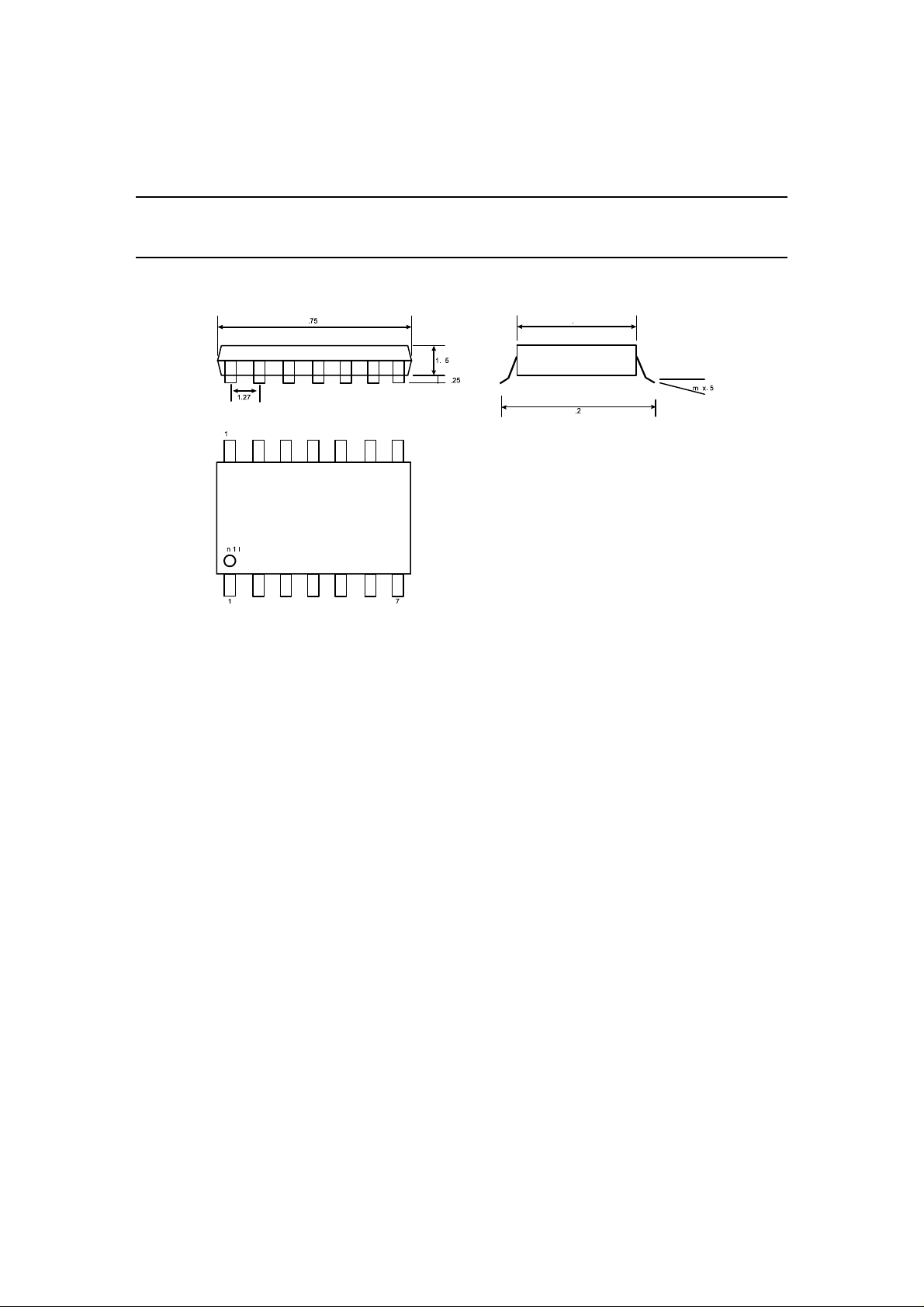
13 PACKAGE
Rev. 1.1 16
Page 17

Philips Semiconductors Product Specification
Hitag Reader Chip HTRC110
14 DEFIN IT IO NS
Amplitudes of sine shap ed sign als: Û, Î
Peak-to-peak of arbitrar y shap ed sig nals: U
Zero-to peak of arbitra ry sh ape d signa ls: Up, I
Data sheet status
Objective specification This data sheet contains tar get or goal specifications for product development .
Preliminary specification This data sheet contains preliminary data; supplementar y data may be published later.
Product specification This data sheet contains final product specifications.
Limiting values
Limiting values given are in accordance with the Absolute Maximum Rating System (IEC 134). Stress above one or
more of the limiting values may cause permanent damage to the device. These are stress ratings only and operation
of the device at these or at any other conditions above those given in the Characteristics sections of the specification
is not implied. Exposure to limiting values for extended periods may affect device reliability.
Application information
Where application information is given, it is advisory and does not form part of the specification.
15 LIFE SUPPORT APPLICATIONS
These products are not designed for use in life support appliances, devices, or systems where malfunction of these
products can reasonably be expected to result in personal injury. Philips customers using or selling these products for
use in such applications do so at their own risk and agree to fully indemnify Philips for any damages resulting from such
improper use or sale.
, I
pp
pp
p
Rev. 1.1 17
Page 18

Philips Semiconductors – a worldwide company
Argentina: see South America
Australia: 34 Waterloo Road, NORTH RYDE, NSW 2113,
Tel. +61 2 9805 4455, Fax. +61 2 9805 4466
Austria: Computerstr. 6, A-1101 WIEN, P.O. Box 213, Tel. +43 160 1010,
Fax. +43 160 101 1210
Belarus: Hotel Minsk Business Center, Bld.3, r. 1211, Volodarski Str. 6,
220050 MINSK, Tel. +375 172 200 733, Fax. +375 172 200 773
Belgium: see The Netherlands
Brazil: see South America
Bulgaria: Philips Bulgaria Ltd., Energoproject, 15th floor,
51 James Bourchier Blvd., 1407 SOFIA,
Tel. +359 2 689 211, Fax. +359 2 689 102
Canada: PHILIPS SEMICONDUCTORS/COMPONENTS,
Tel. +1 800 234 7381
China/Hong Kong: 501 Hong Kong Industrial Technology Centre,
72 Tat Chee Avenue, Kowloon Tong, HONG KONG,
Tel. +852 2319 7888, Fax. + 852 2319 7700
Colombia: see South America
Czech Republic: seeAustria
Denmark: PragsBoulevard 80, PB 1919, DK-2300 COPENHAGEN S,
Tel. +45 32 88 2636, Fax. +45 31 57 0044
Finland: Sinikalliontie 3, FIN-02630 ESPOO,
Tel. +358 9 615800, Fax. +358 9 61580920
France: 4 Rue du Port-aux-Vins, BP317, 92156 SURESNES Cedex,
Tel. +33 1 40 99 6161, Fax. +33 1 40 99 6427
Germany: Hammerbrookstraße 69, D-20097 HAMBURG,
Tel. +49 40 23 53 60, Fax. +49 40 23 536 300
Greece: No. 15, 25th March Street, GR 17778 TAVROS/ATHENS,
Tel. +30 1 4894 339/239, Fax. +30 1 4814 240
Hungary: see Austria
India: Philips INDIA Ltd, Band Box Building, 2nd floor,
254-D, Dr. Annie Besant Road, Worli, MUMBAI 400 025,
Tel. +91 22 493 8541, Fax. +91 22 493 0966
Indonesia: seeSingapore
Ireland: Newstead, Clonskeagh, DUBLIN 14,
Tel. +353 1 7640 000, Fax. +353 1 7640 200
Israel: RAPACElectronics, 7 Kehilat Saloniki St, PO Box 18053,
TEL AVIV 61180, Tel.+972 3 645 0444, Fax. +972 3 649 1007
Italy: PHILIPS SEMICONDUCTORS, Piazza IV Novembre 3,
20124 MILANO, Tel. +39 2 6752 2531, Fax. +39 2 6752 2557
Japan: PhilipsBldg 13-37, Kohnan 2-chome, Minato-ku, TOKYO 108,
Tel. +81 3 3740 5130, Fax. +81 3 3740 5077
Korea: Philips House, 260-199 Itaewon-dong, Yongsan-ku, SEOUL,
Tel. +82 2 709 1412, Fax. +82 2 709 1415
Malaysia: No. 76 J alan Universiti, 46200 PETALING JAYA, SELANGOR,
Tel. +60 3 750 5214, Fax. +60 3 757 4880
Mexico: 5900 Gateway East, Suite 200, EL PASO, TEXAS 79905,
Tel. +9-5 800 234 7381
Middle East: see Italy
Netherlands: Postbus 90050, 5600 PB EINDHOVEN, Bldg. VB,
Tel. +31 40 27 82785, Fax. +31 40 27 88399
New Zealand: 2 Wagener Place, C.P.O. Box 1041, AUCKLAND,
Tel. +64 9 849 4160, Fax. +64 9 849 7811
Norway: Box1, Manglerud 0612, OSLO,
Tel. +47 22 74 8000, Fax. +47 22 74 8341
Philippines: Philips Semiconductors Philippines Inc.,
106 Valero St. Salcedo Village, P.O. Box 2108 MCC, MAKATI,
Metro MANILA, Tel. +63 2 816 6380, Fax. +63 2 817 3474
Poland: Ul. Lukiska 10, PL 04-123 WARSZAWA,
Tel. +48 22 612 2831, Fax. +48 22 612 2327
Portugal: see S pain
Romania: seeItaly
Russia: Philips Russia, Ul. Usatcheva 35A, 119048 MOSCOW,
Tel. +7 095 755 6918, Fax. + 7 095 755 6 919
Singapore: Lorong1, Toa Payoh, SINGAPORE 1231,
Tel. +65 350 2538, Fax. +65 251 6500
Slovakia: see Austria
Slovenia: seeItaly
South Africa: S.A. PHILIPS Pty Ltd., 195-215Main Road Martindale,
2092 JOHANNESBURG, P.O. Box 7430 Johannesburg 2000,
Tel. +27 11 470 5911, Fax. +27 11 470 5494
South America: Rua do Rocio 220, 5th floor, Suite 51,
04552-903 São Paulo, SÃO PAULO - SP, Brazil,
Tel. +55 11 821 2333, Fax. +55 11 829 1849
Spain: Balmes 22, 08007 BARCELONA,
Tel. +34 3 301 6312, Fax. +34 3 301 4107
Sweden: Kottbygatan 7, Akalla, S-16485 STOCKHOLM,
Tel. +46 8 632 2000, Fax. +46 8 632 2745
Switzerland: Allmendstrasse140, CH-8027 ZÜRICH,
Tel. +41 1 488 2686, Fax. +41 1 481 7730
Taiwan: Philips Semiconductors, 6F, No.96, Chien Kuo N. Rd., Sec. 1,
TAIPEI, Taiwan Tel. +886 2 2134 2865, Fax. +886 2 2134 2874
Thailand: PHILIPS ELECTRONICS (THAILAND) Ltd.,
209/2 Sanpavuth-BangnaRoad Prakanong, BANGKOK 10260,
Tel. +66 2 745 4090, Fax. +66 2 398 0793
Turkey: Talatpasa Cad. No.5, 80640 GÜLTEPE/ISTANBUL,
Tel. +90 212 279 2770, Fax. +90 212 282 6707
Ukraine: PHILIPS UKRAINE, 4 Patrice Lumumba str., BuildingB, Floor 7,
252042 KIEV, Tel. +380 44 264 2776, Fax. +380 44 268 0461
United Kingdom: Philips Semiconductors Ltd., 276Bath Road, Hayes,
MIDDLESEX UB3 5BX, Tel. +44 181 730 5000, Fax. +44 181 754 8421
United States: 811East Arques Avenue, SUNNYVALE, CA 94088-3409,
Tel. +1 800 234 7381
Uruguay: see South America
Vietnam: see Singapore
Yugoslavia: PHILIPS, Trg N. Pasica 5/v, 11000 BEOGRAD,
Tel. +381 11 625 344, Fax.+381 11 635 777
For all other countries apply to: Philips Semiconductors, Marketing& Sales Communications,
Building BE-p, P.O. Box 218, 5600 MD EINDHOVEN, The Netherlands, Fax. +31 40 27 24825
© Philips Electronics N.V. 1997 SCA55
All rights are reserved. Reproduction in whole or in part is prohibited without the prior written consent of the copyright owner.
The information presented in this document does not form par t of any quotation or contract, is believed to be accurate and reliable and may be changed
without notice. No liability will be accepted by the publisher for any consequence of its use. Publication thereof does not convey nor imply any license
under patent- or other industrial or intellectual property rights.
Internet: http://www.semiconductors.philips.com
 Loading...