

Page 1

Doc. No. 1213, Rev. 1
January 20, 1999
5+'3&,
+RVW&RQWUROOHG9.IOH[
0RGHP'HYLFH)DPLO\IRU'HVNWRS$SSOLFDWLRQV
'HVLJQHU}V*XLGH
Conexant Proprietary Information
Dissemination or use of this information is not permitted
without the written permission of Conexant Systems, Inc.
Page 2

RH56D-PCI Modem Designer’s Guide
ii
Conexant
1213
Conexant Proprietary Information
Information provided by Conexant Sys t ems, Inc. is believed to be accurat e and reliable. However, no responsibility is assumed by Conexant
for its use, nor any infri ngem ent of patents or other rights of third parties which may result from its use. No lic ense is granted by implicat i on or
otherwise under any patent rights of Conexant other than for circui t ry embodied in Conexant products. Conexant reserves the right to change
circuitry at any ti m e without notice. This docum ent is subject to change wit hout notice.
K56flex is a trademark of Conexant Systems, I nc. and Lucent Technologies.
Conexant and “What's Next in Comm uni cations Technologies” are trademark s of Conexant Systems , Inc.
Product names or servic es listed in this public ation are for identification purpos es only, and may be trademarks or regi stered trademarks of
their respective compani es. All other marks ment i oned herei n are the property of their respective owners.
©1999, Conexant Systems , Inc.
Printed in U.S.A.
All Rights Reserved
Page 3

RH56D-PCI Modem Designer’s Guide
1213
Conexant
iii
Conexant Proprietary Information
Table of Contents
1. INTRODUCTION................................................................................................................................................. 1-1
1.1 SUMMARY............................................................................................................................................... 1-1
1.2 FEATURES.............................................................................................................................................. 1-3
1.3 TECHNICAL OVERVIEW......................................................................................................................... 1-6
1.3.1 General Description...................................................................................................................1-6
1.3.2 Host Modem Software................................................................................................................ 1-6
1.3.3 Operating Modes........................................................................................................................ 1-6
Data/Fax Modes................................................................................................................ 1-6
Synchronous Access Mode (SAM) - Video Conferencing................................................. 1-6
Voice/TAM Mode............................................................................................................... 1-7
Speakerphone Mode (SP Model)...................................................................................... 1-7
1.3.4 Hardware Interfaces................................................................................................................... 1-7
PCI Bus Host Interface...................................................................................................... 1-7
Serial EEPROM Interface ................................................................................................. 1-8
Audio Interface.................................................................................................................. 1-8
Telephone Line/Telephone/Audio Interface...................................................................... 1-8
2. TECHNICAL SPECIFICATIONS ........................................................................................................................ 2-1
2.1 ESTABLISHING DATA MODEM CONNECTIONS................................................................................... 2-1
Dialing............................................................................................................................... 2-1
Modem Handshaking Protocol.......................................................................................... 2-1
Call Progress Tone Detection........................................................................................... 2-1
Answer Tone Detection..................................................................................................... 2-1
Ring Detection................................................................................................................... 2-1
Billing Protection ............................................................................................................... 2-1
Connection Speeds........................................................................................................... 2-1
Automode.......................................................................................................................... 2-1
2.2 DATA MODE............................................................................................................................................ 2-1
Speed Buffering (Normal Mode) .......................................................................................2-1
DTE-to-Modem Flow Control............................................................................................. 2-1
Escape Sequence Detection............................................................................................. 2-1
GSTN Cleardown (V.90/K56flex, V.34, V.32 bis, V.32)..................................................... 2-2
Fall Forward/Fallback (V.90/K56flex, V.34/V.32 bis/V.32)................................................ 2-2
Retrain............................................................................................................................... 2-2
2.3 ERROR CORRECTION AND DATA COMPRESSION............................................................................. 2-2
V.42 Error Correction........................................................................................................ 2-2
MNP 2-4 Error Correction ................................................................................................. 2-2
V.42 bis Data Compression .............................................................................................. 2-2
MNP 5 Data Compression ................................................................................................2-2
2.4 FAX CLASS 1 OPERATION..................................................................................................................... 2-2
2.5 VOICE/TAM MODE.................................................................................................................................. 2-2
2.5.1 Online Voice Command Mode................................................................................................... 2-2
2.5.2 Voice Receive Mode.................................................................................................................. 2-3
2.5.3 Voice Transmit Mode................................................................................................................. 2-3
2.5.4 Speakerphone Modes................................................................................................................ 2-3
2.6 FULL-DUPLEX SPEAKERPHONE (FDSP) MODE.................................................................................. 2-3
2.7 CALLER ID............................................................................................................................................... 2-3
2.8 MULTIPLE COUNTRY SUPPORT........................................................................................................... 2-3
2.8.1 OEM Programmable Parameters............................................................................................... 2-3
2.8.2 Blacklist Parameters.................................................................................................................. 2-3
2.9 DIAGNOSTICS......................................................................................................................................... 2-4
2.9.1 Commanded Tests..................................................................................................................... 2-4
2.10 LOW POWER SLEEP MODE...................................................................................................................2-4
Page 4

RH56D-PCI Modem Designer’s Guide
iv
Conexant
1213
Conexant Proprietary Information
3. HARDWARE INTERFACE ................................................................................................................................. 3-1
3.1 HARDWARE SIGNAL PINS AND DEFINITIONS..................................................................................... 3-1
3.2 POWER REQUIREMENTS AND MAXIMUM RATINGS.........................................................................3-13
3.3 MDP ELECTRICAL CHARACTERISTICS.............................................................................................. 3-14
3.4 PCI BUS ELECTRICAL, SWITCHING, AND TIMING CHARACTERISTICS.......................................... 3-14
4. DESIGN CONSIDERATIONS............................................................................................................................. 4-1
4.1 PC BOARD LAYOUT GUIDELINES......................................................................................................... 4-1
4.1.1 General Principles...................................................................................................................... 4-1
4.1.2 Component Placement............................................................................................................... 4-1
4.1.3 Signal Routing............................................................................................................................ 4-2
4.1.4 Power......................................................................................................................................... 4-3
4.1.5 Ground Planes........................................................................................................................... 4-4
4.1.6 Crystal Circuit............................................................................................................................. 4-4
4.1.7 VC and VREF Circuit ................................................................................................................. 4-4
4.1.8 Telephone and Local Handset Interface.................................................................................... 4-5
4.1.9 Optional Configurations ............................................................................................................. 4-5
4.1.10 MDP Specific.............................................................................................................................. 4-5
4.2 CUSTOM DESIGN GUIDELINES FOR 2-LAYER PCI MODEM BOARD................................................. 4-5
4.2.1 General Guidelines.................................................................................................................... 4-5
4.2.2 Placement of Modem Devices ................................................................................................... 4-6
4.2.3 Trace Routing and Length on PCI Signals................................................................................. 4-6
4.2.4 Grounding.................................................................................................................................. 4-6
4.2.5 Filtering...................................................................................................................................... 4-6
4.2.6 Decoupling................................................................................................................................. 4-7
4.2.7 Crystal Circuit............................................................................................................................. 4-7
4.2.8 Modem Analog Interface............................................................................................................ 4-8
4.3 PCB LAYOUT EXAMPLES
....................................................................................................................... 4-9
4.4 CRYSTAL/OSCILLATOR SPECIFICATIONS ........................................................................................4-11
4.5 OTHER CONSIDERATIONS.................................................................................................................. 4-11
4.6 PACKAGE DIMENSIONS....................................................................................................................... 4-14
5. SOFTWARE INTERFACE.................................................................................................................................. 5-1
5.1 PCI CONFIGURATION REGISTERS....................................................................................................... 5-1
5.1.1 0x00 - Vendor ID Field............................................................................................................... 5-1
5.1.2 0x02 - Device ID Field................................................................................................................ 5-1
5.1.3 0x04 - Command Register......................................................................................................... 5-2
5.1.4 0x06 - Status Register ............................................................................................................... 5-2
5.1.5 0x08 - Revision ID Field............................................................................................................. 5-3
5.1.6 0x09 - Class Code Field............................................................................................................. 5-3
5.1.7 0x0D - Latency Timer Register .................................................................................................. 5-3
5.1.8 0x0E - Header Type Field.......................................................................................................... 5-3
5.1.9 0x28 - CIS Pointer Register ....................................................................................................... 5-3
5.1.10 0x2C - Subsystem Vendor ID Register...................................................................................... 5-3
5.1.11 0x2E- Subsystem ID Register.................................................................................................... 5-3
5.1.12 0x34 - Cap Ptr............................................................................................................................ 5-3
5.1.13 0x3C - Interrupt Line Register.................................................................................................... 5-3
5.1.14 0x3D - Interrupt Pin Register...................................................................................................... 5-3
5.1.15 0x3E - Min Grant Register.......................................................................................................... 5-3
5.1.16 0x3F - Max Latency Register..................................................................................................... 5-3
5.1.17 0x40 - Capability Identifier ......................................................................................................... 5-3
5.1.18 0x41 - Next Item Pointer ............................................................................................................ 5-3
5.1.19 0x42 - PMC - Power Management Capabilities ......................................................................... 5-4
5.1.20 0x44 - PMCSR - Power Management Control/Status Register (Offset = 4)............................... 5-4
5.1.21 0x46 - PMCSR_BSE - PMCSR PCI to PCI Bridge Support Extensions..................................... 5-4
5.1.22 0x47 - Data ................................................................................................................................ 5-4
Page 5

RH56D-PCI Modem Designer’s Guide
1213
Conexant
v
Conexant Proprietary Information
5.2 BASE ADDRESS REGISTER .................................................................................................................. 5-5
5.3 SERIAL EEPROM INTERFACE............................................................................................................... 5-6
5.3.1 Supported EEPROM Sizes........................................................................................................ 5-6
5.3.2 Definitions.................................................................................................................................. 5-7
Device ID Register............................................................................................................ 5-7
Vendor ID Register............................................................................................................ 5-7
Subsystem Vendor ID and Subsystem Device Register................................................... 5-7
Min_Gnt Register.............................................................................................................. 5-7
Max_Lat Register.............................................................................................................. 5-7
PMC [8:6], PME DRV Type............................................................................................... 5-8
CardBus CIS Pointer (CardBus CIS pointer High, CardBus CIS pointer Low).................. 5-8
Data Register (D3, D2, D1, D0 power consumed and D3, D2, D1, D0 power
dissipated)......................................................................................................................... 5-8
Load CISRAM Count (CIS _SIZE) .................................................................................... 5-8
Page 6

RH56D-PCI Modem Designer’s Guide
vi
Conexant
1213
Conexant Proprietary Information
List of Figures
Figure 1-1. RH56D-PCI System Overview ............................................................................................................................... 1-4
Figure 1-2. RH56D-PCI Hardware Configuration Block Diagram............................................................................................. 1-5
Figure 1-3. Typical Audio Signal Interface (U.S.)..................................................................................................................... 1-9
Figure 3-1. RH56D-PCI Major Hardware Interface Signals...................................................................................................... 3-2
Figure 3-2. R6795 144-Pin TQFP Hardware Interface Signals................................................................................................ 3-3
Figure 3-3. R6795 144-Pin TQFP Pin Signals.......................................................................................................................... 3-4
Figure 3-4. Schematic - R6795 Interface –Speakerphone Application................................................................................... 3-12
Figure 4-1. PCICLK Guard Band Technique............................................................................................................................ 4-9
Figure 4-2. Receive Path Guard-Band, Merge between AGND-GND...................................................................................... 4-9
Figure 4-3. Crystal Solution.................................................................................................................................................... 4-10
Figure 4-4. Power and Ground Distribution............................................................................................................................ 4-10
Figure 4-5. Package Dimensions - 144-Pin TQFP................................................................................................................. 4-14
List of Tables
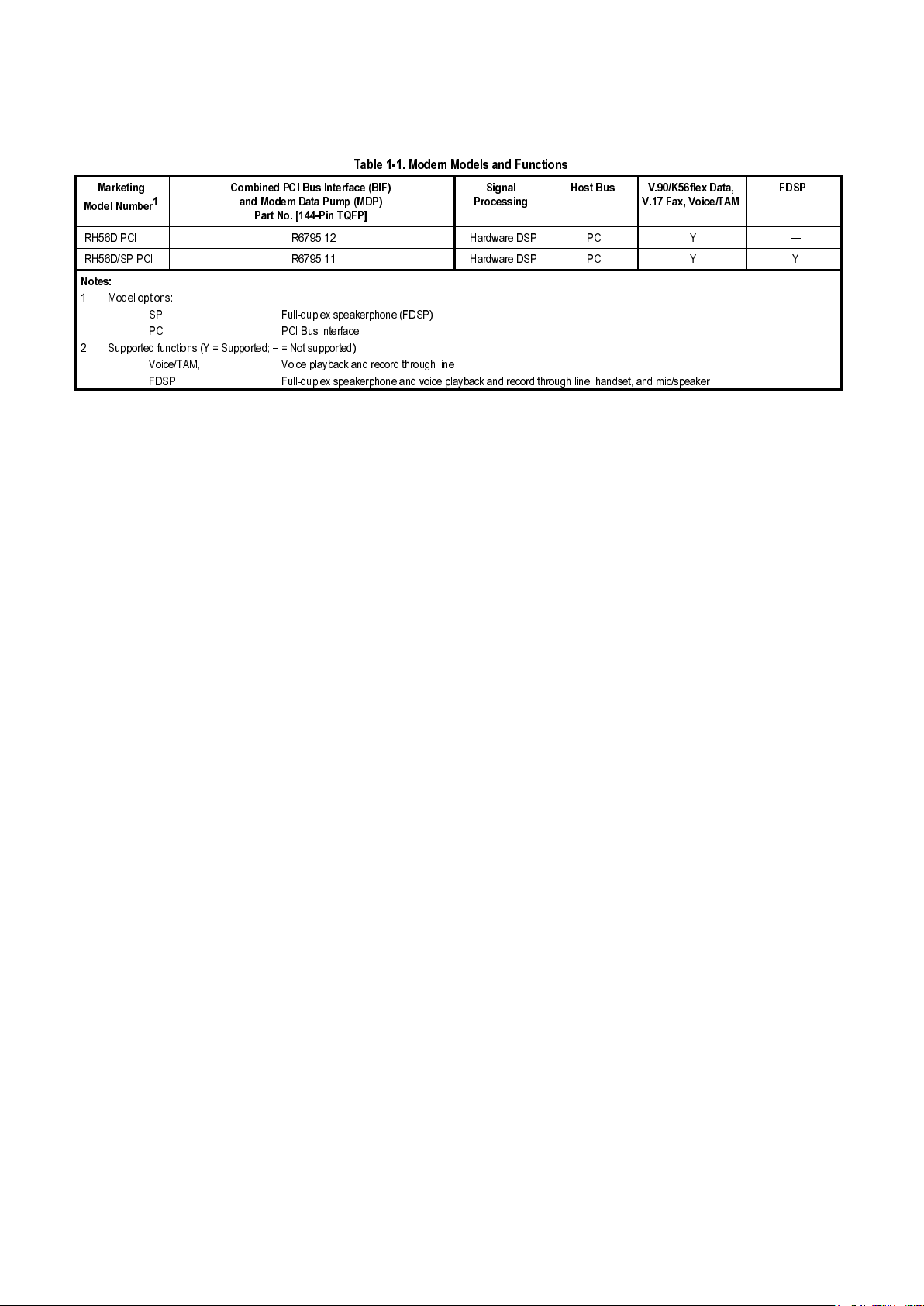
Table 1-1. Modem Models and Functions................................................................................................................................ 1-2
Table 1-2. Typical Signal Routing - Voice Mode .................................................................................................................... 1-10
Table 3-1. R6795 144-Pin TQFP Pin Signals ........................................................................................................................... 3-5
Table 3-2. R6795 Pin Signal Definitions................................................................................................................................... 3-7
Table 3-3. Current and Power Requirements......................................................................................................................... 3-13
Table 3-4. Absolute Maximum Ratings................................................................................................................................... 3-13
Table 3-5. Analog Electrical Characteristics........................................................................................................................... 3-14
Table 4-1. Crystal Specifications - Surface Mount ................................................................................................................. 4-12
Table 4-2. Crystal Specifications - Through Hole................................................................................................................... 4-13
Table 5-1. PCI Configuration Registers.................................................................................................................................... 5-1
Table 5-2. Command Register ................................................................................................................................................. 5-2
Table 5-3. Status Register........................................................................................................................................................ 5-2
Table 5-4. Power Management Capabilities (PMC) Register................................................................................................... 5-4
Table 5-5. Power Management Control/Status Register (PMCSR).......................................................................................... 5-4
Table 5-6. BIF Address Map..................................................................................................................................................... 5-5
Table 5-7. EEPROM Content for 256 Words by 16 Bits per Word........................................................................................... 5-6
Table 5-8. EEPROM Content for 128 Words by 16 Bits per Word........................................................................................... 5-6
Page 7

RH56D-PCI Modem Designer’s Guide
1213
Conexant
1-1
Conexant Proprietary Information
1. INTRODUCTION
1.1 SUMMARY
The Conexant RH56D-PCI V.90/K56flex Host Controlled Modem Device Family supports high speed analog data up to 56
kbps, 14.4 kbps fax, voice/TAM, and speakerphone (optional) operation. The modem operates with PSTN telephone lines in
the U.S. and world-wide. The modem is available with or without speakerphone support (see Table 1-1).
The modem is packaged in a single 144-pin thin quad flat pack (TQFP) that combines PCI Bus Interface (BIF) and Modem
Data Pump (MDP) functions.
This modem is pin-compatible with the SoftK56-PCI modem, part number R6793 (see
SoftK56-PCI data sheet Order No. MD231).
Host modem software is also provided.
Operating with +3.3V power, this device set supports 32-bit host applications in such designs as embedded motherboards
and PCI half cards. Downloadable architecture allows updating of MDP executable code.
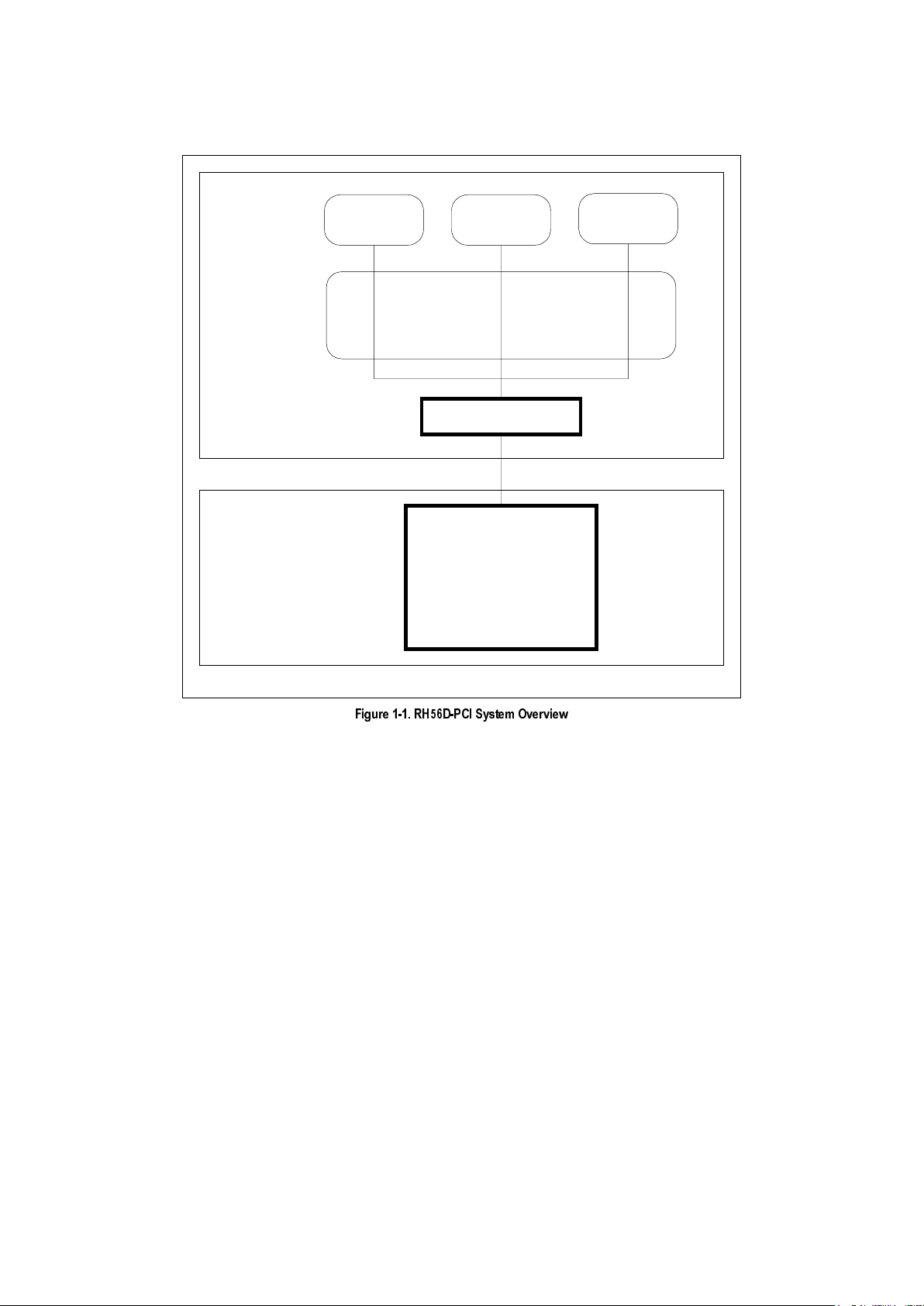
Figure 1-1 illustrates the general structure of the RH56D-PCI software and the interface to the RH56D-PCI hardware.
Figure 1-2 illustrates the major hardware interfaces supported by each model.
In ITU-T V.90/K56flex data mode, the modem can receive data at speeds up to 56 kbps from a digitally connected V.90 or
K56flex-compatible central site modem. A V.90/K56flex modem takes advantage of the PSTN which is primarily digital except
for the client modem to central office local loop and is ideal for applications such as remote access to an Internet Service
Provider (ISP), on-line service, or corporate site. In this mode, the modem can transmit data at speeds up to V.34 rates.
In V.34 data mode, the modem operates at line speeds up to 33.6 kbps. When applicable, error correction (V.42/MNP 2-4)
and data compression (V.42 bis/MNP 5) maximize data transfer integrity and boost average data throughput. Non-errorcorrecting mode is also supported.
All models support remote audio recording and remote audio playback over the telephone line interface using A-Law, µ-Law,
or linear coding at 8000 or 7200 Hz sample rate to support applications such as digital telephone answering machine (TAM).
The SP model supports position independent, full-duplex speakerphone (FDSP) operation.
Fax Group 3 send and receive rates are supported up to 14.4 kbps with T.30 protocol.
V.80 synchronous access mode supports host-controlled communication protocols, e. g., H.324 video conferencing.
Reference design kits are available to minimize application design time and costs.
This designer's guide describes the modem hardware capabilities and identifies the supporting commands. Commands and
parameters are defined in the Commands for RH56D/RC56HCF and RH56LD Reference Manual (Order No. 1118).
Page 8
RH56D-PCI Modem Designer’s Guide
1-2
Conexant
1213
Conexant Proprietary Information
7DEOH 0RGHP 0RGHOV DQG )XQFWLRQV
0DUNHWLQJ
0RGHO 1XPEHU
&RPELQHG 3&, %XV ,QWHUIDFH %,)
DQG 0RGHP 'DWD 3XPS 0'3
3DUW 1R >3LQ 74)3@
6LJQDO
3URFHVVLQJ
+RVW %XV 9.IOH[ 'DWD
9 )D[ 9RLFH7$0
)'63
5+'3&, 5 +DUGZDUH '63 3&, < ²
5+'633&, 5 +DUGZDUH '63 3&, < <
1RWHV
0RGHO RSWLRQV
63 )XOOGXSOH[ VSHDNHUSKRQH )'63
3&, 3&, %XV LQWHUIDFH
6XSSRUWHG IXQFWLRQV < 6XSSRUWHG ± 1RW VXSSRUWHG
9RLFH7$0 9RLFH SOD\EDFN DQG UHFRUG WKURXJK OLQH
)'63 )XOOGXSOH[ VSHDNHUSKRQH DQG YRLFH SOD\EDFN DQG UHFRUG WKURXJK OLQH KDQGVHW DQG PLFVSHDNHU
Page 9

RH56D-PCI Modem Designer’s Guide
1213
Conexant
1-3
Conexant Proprietary Information
1.2 FEATURES
•
Data modem
−
ITU-T V.90, K56flex, V.34 (33.6 kbps), V.32 bis, V.32, V.22 bis, V.22, V.23, and V.21; Bell 212A and 103
−
V.42 LAPM and MNP 2-4 error correction
−
V.42 bis and MNP 5 data compression
−
V.250 (ex V.25 ter) and V.251 (ex V.25 ter Annex A) commands
−
Fax modem send and receive rates up to 14.4 kbps ITU-T V.17, V.29, V.27 ter, and V.21 channel 2
−
EIA/TIA 578 Class 1 and T.31 Class 1.0 commands
•
Voice, telephony, TAM
−
V.253 commands
−
8-bit µ-Law/A-Law coding (G.711)
−
8-bit/16-bit linear coding
−
8000/7200 Hz sample rate
−
Music on hold from host or analog hardware input
−
TAM support with concurrent DTMF detect, ring detect and caller ID
•
V.80 synchronous access mode supports host-controlled communication protocols
−
H.324 interface support
•
V.8/V.8bis and V.251 (ex V.25 ter Annex A) commands
•
Full-duplex Speakerphone (FDSP) Mode (SP model)
−
Telephone handset interface
−
External microphone and speaker interface
−
Microphone gain and muting
−
Speaker volume control and muting
−
Adaptive acoustic, line, and handset echo cancellation
−
Loop gain control, transmit and receive path AGC
•
Data/Fax/Voice call discrimination
•
Multiple country support
−
Call progress, blacklisting
•
Single profile stored in host
•
Modem and audio paths concurrent across PCI Bus
•
System compatibilities
−
Windows 95, Windows 95 OSR2, Windows 98, Windows NT 4.0, Windows NT 5.0 operating systems
−
Microsoft's PC 98 Design Initiative compliant
−
Unimodem/V compliant
−
Pentium 133 MHz equivalent or greater
−
16 Mbyte RAM or more
•
32-bit PCI Local Bus interface
−
Conforms to the PCI Local Bus Specification, Production Version, Revision 2.1
−
PCI Bus Mastering interface to the MDP
−
33 MHz PCI clock support
•
Supports PCI Bus Power Management
−
Conforms to PCI Bus Power Management Specification, Rev. 1.1
−
ACPI Power Management Registers
−
APM support
−
PME# support
•
Device package
−
R6795 Modem: 144-pin TQFP (1.6 mm max. height)
•
+3.3V operation with +5V tolerant digital inputs
•
+5V or +3.3V analog operation
Page 10
RH56D-PCI Modem Designer’s Guide
1-4
Conexant
1213
Conexant Proprietary Information
RH56D-PCI
Serial Port Driver*
Win95
Communications Stack
*CONEXANT supplied
Modem Hardware
on Motherboard
or Plug-in Module
1213F1 SO
PC Software
Win32-based
communications
application
Win16-based
communications
application
MS-DOS
application
(MS-DOS Box)
RH56D-PCI
Modem Device Hardware*
Bus Interface (BIF)
and
Modem Data Pump (MDP)
Functions
)LJXUH 5+'3&, 6\VWHP 2YHUYLHZ
Page 11
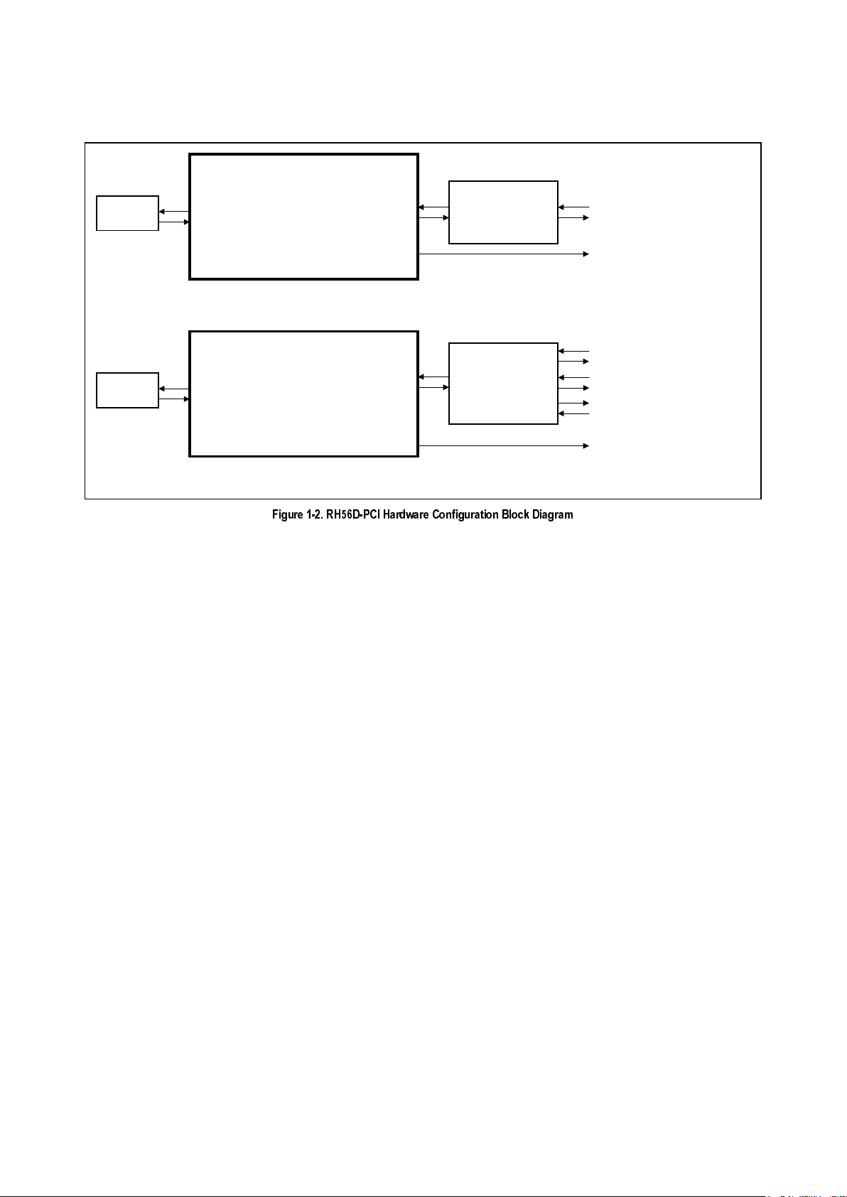
RH56D-PCI Modem Designer’s Guide
1213
Conexant
1-5
Conexant Proprietary Information
MD239F1 BD
a. Typical Interface for Data/Fax/Remote TAM
b. Typical Interface for Data/Fax/Voice/Speakerphone
RH56D-PCI MODEM DEVICE
COMBINED PCI BUS INTERFACE
AND MODEM DATA PUMP
[R6795-12: 144-PIN TQFP]
PCI BUS
PSTN
TELEPHONE LINE
TELEPHONE LINE/
TELEPHONE HANDSET/
MIC AND SPEAKER
INTERFACE CIRCUIT
RH56D/SP-PCI MODEM DEVICE
COMBINED PCI BUS INTERFACE
AND MODEM DATA PUMP
[R6795-11: 144-PIN TQFP]
PCI BUS
PSTN
TELEPHONE LINE
SPEAKER (OPTIONAL) [SP MODEL]
TELEPHONE LINE/
TELEPHONE HANDSET/
MIC AND SPEAKER
INTERFACE CIRCUIT
MIC (OPTIONAL) [SP MODEL]
HANDSET (OPTIONAL) [SP MODEL]
DIGITAL SPEAKER
(CALL PROGRESS)
DIGITAL SPEAKER
(CALL PROGRESS)
)LJXUH 5+'3&, +DUGZDUH &RQILJXUDWLRQ %ORFN 'LDJUDP
Page 12

RH56D-PCI Modem Designer’s Guide
1-6
Conexant
1213
Conexant Proprietary Information
1.3 TECHNICAL OVERVIEW
1.3.1 General Description
The RH56D-PCI modem provides the processing core for a complete system design featuring data/fax modem, voice/TAM,
and speakerphone support, depending on specific model (Table 1-1).
Note:
The term, “RH56D-PCI Device Set”, refers to the family of modem models listed in Table 1-1.
Modem operation, including dialing, call progress, telephone line interface, telephone handset interface, audio interface, and
host interface functions are supported and controlled through the command set.
The modem hardware connects to the host processor via a PCI Bus interface. The OEM adds a crystal circuit, EEPROM,
telephone line interface, telephone handset interface (optional), and audio interface (optional) to complete the system.
1.3.2 Host Modem Software
The host modem software performs two distinct tasks:
1. General modem control which includes command sets, fax Class 1, voice/TAM, speakerphone, error correction, data
compression, and operating system interface functions.
2. Modem data pump control. Binary executable code controlling MDP operation is downloaded as required during
operation.
Configurations of the modem software are provided to support modem models listed in Table 1-1.
Binary executable modem software is provided for the OEM.
1.3.3 Operating Modes
Data/Fax Modes
As a V.90/K56flex data modem, the modem can receive data from a digital source using a V.90- or K56flex-compatible central
site modem over the digital telephone network portion of the PSTN at line speeds up to 56 kbps. Asymmetrical data
transmission supports sending data up to V.34 rates. This mode can fallback to full-duplex V.34 mode, and to slower rates as
dictated by line conditions.
As a V.34 data modem, the modem can operate in 2-wire, full-duplex, asynchronous modes at line rates up to 33.6 kbps.
Data modem modes perform complete handshake and data rate negotiations. Using V.34 modulation to optimize modem
configuration for line conditions, the modem can connect at the highest data rate that the channel can support from 33600
bps down to 2400 bps with automatic fallback. Automode operation in V.34 is provided in accordance with PN3320 and in
V.32 bis in accordance with PN2330. All tone and pattern detection functions required by the applicable ITU or Bell standard
are supported.
In fax modem mode, the modem can operate in 2-wire, half-duplex, synchronous modes and can support Group 3 facsimile
send and receive speeds of 14400, 12000, 9600, 7200, 4800, or 2400 bps. Fax data transmission and reception performed
by the modem are controlled and monitored through the fax EIA/IA-578 Class 1 and T.31 Class 1.0 command interface. Full
HDLC formatting, zero insertion/deletion, and CRC generation/checking are provided.
Both transmit and receive fax data are buffered within the modem. Data transfer to and from the DTE is flow controlled by
XON/XOFF and RTS/CTS.
Synchronous Access Mode (SAM) - Video Conferencing
V.80 synchronous access mode between the modem and the host/DTE is provided for host-controlled communication
protocols, e.g., H.324 video conferencing applications.
Voice-call-first (VCF) before switching to a videophone call is also supported.
Page 13

RH56D-PCI Modem Designer’s Guide
1213
Conexant
1-7
Conexant Proprietary Information
Voice/TAM Mode
Voice/TAM Mode features include 8-bit µ-Law, A-Law, and linear coding at 8000 Hz and 7200 Hz sample rates. Tone
detection/generation, call discrimination, and concurrent DTMF detection are also supported. ADPCM (4-bit IMA) coding is
also supported to meet Microsoft WHQL logo requirements.
Voice/TAM Mode is supported by three submodes:
1. Online Voice Command Mode supports connection to the telephone line or, for the SP model, a handset.
2. Voice Receive Mode supports recording voice or audio data input at the RIN pin, typically from the telephone line or, for
the SP model, a microphone/handset.
3. Voice Transmit Mode supports playback of voice or audio data to the TXA1/TXA2 output, typically to the telephone line
or, for the SP model, a speaker/handset.
Speakerphone Mode (SP Model)
The SP model includes additional telephone handset, external microphone, and external speaker interfaces which support
voice and full-duplex speakerphone (FDSP) operation.
Hands-free full-duplex telephone operation is supported in Speakerphone Mode under host control. Speakerphone Mode
features an advanced proprietary speakerphone algorithm which supports full-duplex voice conversation with acoustic, line,
and handset echo cancellation. Parameters are constantly adjusted to maintain stability with automatic fallback from fullduplex to pseudo-duplex operation. The speakerphone algorithm allows position independent placement of microphone and
speaker. The host can separately control volume, muting, and AGC in microphone and speaker channels.
1.3.4 Hardware Interfaces
PCI Bus Host Interface
The Bus Interface conforms to the PCI Local Bus Specification, Production Version, Revision 2.1, June 1, 1995. It is a
memory slave (burst transactions) and a bus master for PC host memory accesses (burst transactions). Configuration is by
PCI configuration protocol.
The following interface signals are supported:
•
Address and data
−
32 bidirectional Address/Data (AD[31-0]; bidirectional
−
Four Bus Command and Byte Enable (CBE [3:0]), bidirectional
−
Bidirectional Parity (PAR); bidirectional
•
Interface control
−
Cycle Frame (FRAME#); bidirectional
−
Initiator Ready (IRDY#); bidirectional
−
Target Ready (TRDY#); bidirectional
−
Stop (STOP#); bidirectional
−
Initialization Device Select (IDSEL); input
−
Device Select (DEVSEL#); bidirectional
•
Arbitration
−
Request (REQ#); output
−
Grant (GRANT#); input
•
Error reporting
−
Parity Error (PERR#); bidirectional
−
System Error ; bidirectional
•
System
−
Interrupt A (INTA#); output
−
Clock (PCICLK); input
−
Reset (PCIRST#); input
•
Power Management
−
Power Management Event (PME#), output
−
Vaux Detect (VauxDET), input
Page 14

RH56D-PCI Modem Designer’s Guide
1-8
Conexant
1213
Conexant Proprietary Information
Serial EEPROM Interface
A serial EEPROM is required to store the Maximum Latency, Minimum Grant, Device ID, Vendor ID, Subsystem ID, and
Subsystem Vendor ID parameters for the PCI Configuration Space Header.
The serial EEPROM interface connects to an
Microchip 93LC66B (
256 x 16)
, 93LC56B (
128 x 16)
, Atmel AT93C66 (
256 x 16),
AT93C56 (
128 x 16), or equivalent serial
EEPROM rated at 1 MHz (SROMCLK is 537.6 kHz). Its size can be reduced from the total of 4096 (256 x 16) bits down to
2048 (128 x 16) bits in non-PC card applications.
The interface signals are: a serial data input line from the EEPROM (SROMIN), a serial data output line to the EEPROM
(SROMOUT), Clock to the EEPROM (SROMCLK), and chip select to the EEPROM (SROMCS).
The EEPROM is
programmable by the PC via the R6795 device (see Section 5.3).
Audio Interface
A digital speaker output (DSPKOUT), or analog speaker output (SPKOUT) available in the SP models, is supported on
separate pins, as selected by a bit in the INF file. Both outputs cannot be active at the same time.
The digital speaker output (DSPKOUT) provides square wave call progress or carrier signals, which can be optionally
connected to a low-cost on-board speaker, e.g., a sounducer, without the use of an external op-amp. This output is used for
call progress in Data/Fax mode only where sound quality is not important.
The MIC_V and SPKOUT lines, supported in SP model, connect to an external microphone and external speaker to support
functions such as speakerphone mode, telephone emulation, microphone voice record, speaker voice playback, and call
progress monitor. The SPKOUT output should be used in speakerphone designs where sound quality is important.
The analog microphone input (MIC_V) can also accept an external audio signal to support functions such as speakerphone
mode, telephone emulation, microphone voice record, and music on hold.
Also, for the SP models, a telephone input (TELIN) is supported for optionally connecting the modem to a telephone handset
microphone and a telephone output (TELOUT) is supported for optionally connecting the modem to a telephone handset
speaker.
Telephone Line/Telephone/Audio Interface
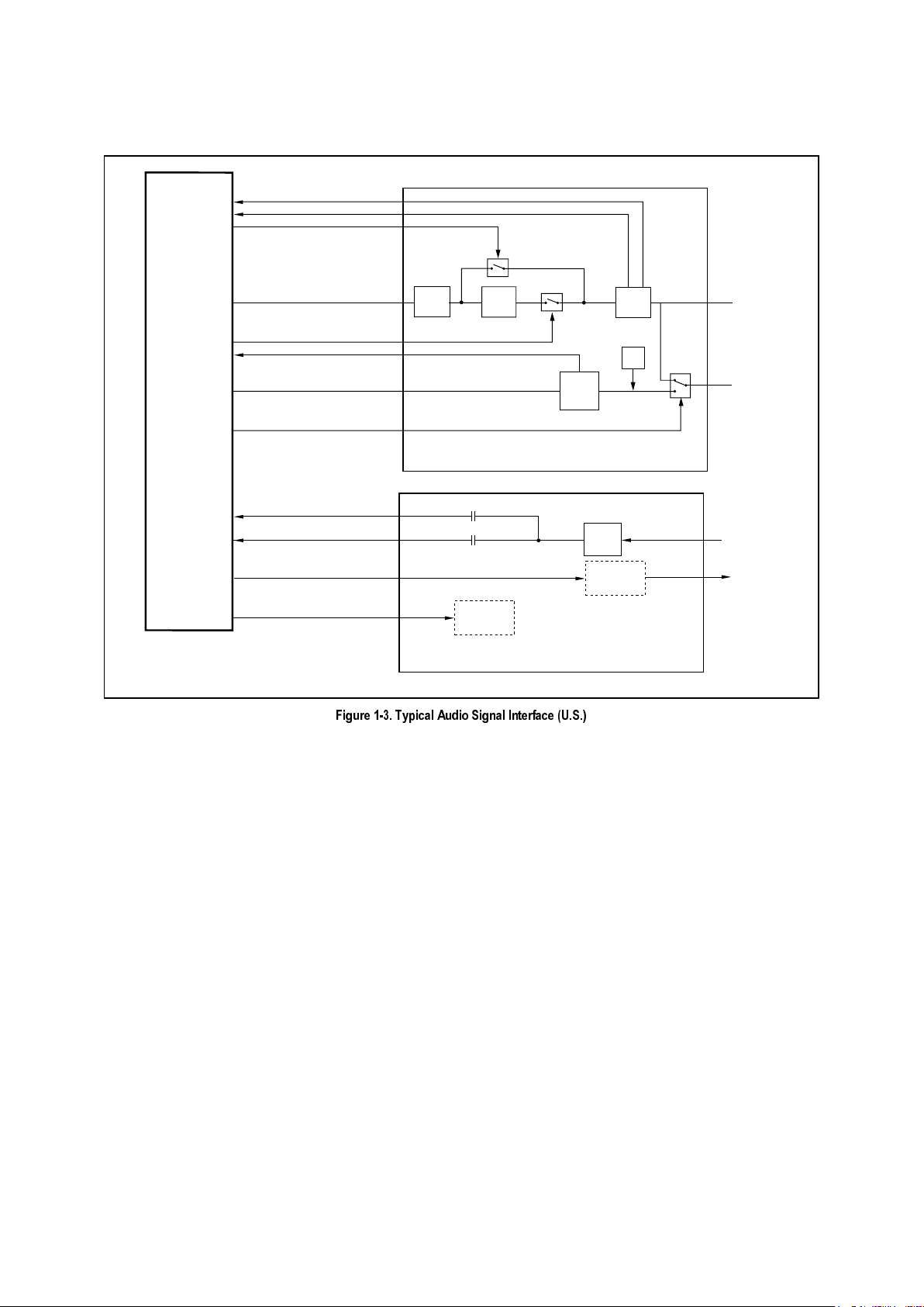
The Telephone Line/Telephone/Audio Signal Interface can support a 3-relay telephone line interface (Figure 1-3). Signal
routing for Voice mode is shown in Table 1-2.
The following signals are supported:
•
A single-ended Receive Analog input (RXA) input and a differential Transmit Analog output (TXA1 and TXA2) output.
•
An Off-hook (OH#) relay control output for connecting the modem to the telephone line.
•
A Caller ID (CID) relay control output for optionally connecting the telephone line to the modem for Caller ID data extraction.
•
A Voice (VOICE#) relay control output for optionally switching the telephone line connection between the modem and the
telephone handset.
•
A Ring Indicate (IRING#) input for sensing a raw incoming ring signal.
•
A Loop Current Sense (LCS#) input for optionally sensing the local primary telephone off-hook status.
•
An Extension Off-Hook (EXT_L#) input for optionally sensing local extension telephone off-hook status.
•
Remote Hang-up (LCS_L#/RH_L#) input for optionally sensing remote telephone off-hook status.
•
Telephone input (TELIN) for connection to a microphone or telephone handset (SP model).
•
Telephone output (TELOUT) for connection to a speaker or telephone handset (SP model).
Page 15
RH56D-PCI Modem Designer’s Guide
1213
Conexant
1-9
Conexant Proprietary Information
MODEM
DEVICE SET
1129F1-3 AIF 3R-US
TELEPHONE LINE/TELEPHONE HANDSET
INTERFACE CIRCUIT
HEADPHONE
MICROPHONE
IRING#
RINGWAKE#
CID#
TXA1/TXA2/RXA
OH#
LCS#
TELIN/TELOUT
VOICE#
BIAS
AUDIO/HEADPHONE
INTERFACE CIRCUIT
SSI
&
BRDGE
OH
RELAY
XFRMR
TEL LINE
TEL HANDSET
VOICE
RELAY
CUR
SRC
RING
DETECT
MIC_M
MIC_V
SPKROUT_M*
SPKMD*
HANDSET
HOOK
STATUS
DETECT
AMP/
SOUNDUCER
(OPTIONAL)
SOUNDUCER
(LOW COST
OPTIONAL)
CID
RELAY
* USE ONLY ONE OUTPUT.
)LJXUH 7\SLFDO $XGLR 6LJQDO ,QWHUIDFH 86
Page 16

RH56D-PCI Modem Designer’s Guide
1-10
Conexant
1213
Conexant Proprietary Information
7DEOH 7\SLFDO 6LJQDO 5RXWLQJ 9RLFH 0RGH
+VLS=
Command
Description Input Selected Output Selected OH#
Output
Activated
VOICE#
Output
Activated
CID#
Output
Activated
0 Modem on hook; phone connected to Line No No Yes
1 Modem connected to Line RXA TXA1/TXA2 Yes Yes No
2 Modem connected to Handset TELIN TELOUT No Yes Yes
3 Modem connected to Line and Handset RXA TXA Yes No No
4 Modem connected to Speaker SPKOUT No No Yes
5 Modem connected to Line and Speaker RXA TXA1/TXA2, SPKOUT Yes Yes No
6 Modem connected to Microphone MIC_V No No Yes
7 Speaker and Mic routed to Line vi a M odem TXA1/TXA2 Yes Y es No
8 Modem connected to Speaker SPKOUT No No Yes
9 Modem connected to Line and Speaker RXA TXA1/TXA2, SPKOUT Yes Yes No
10 Speaker and Mic routed to Line via Modem RXA, MIC_V TXA1/TXA2, SPKOUT Yes Yes No
11 Modem connected to Microphone MIC_V No No Yes
12 Speaker and Mic routed to Line via Modem RXA, MIC_V TXA1/TXA2, SPKOUT Yes Yes No
13 Speaker and Mic routed to Line via Modem RXA, MIC_V TXA1/TXA2, SPKOUT Yes Yes No
14 Modem connected to Headset MIC_V SPKOUT No No Yes
15 Speaker and Mic routed to Li ne via Modem RXA, MIC_V TXA1/TXA2 Yes Y es No
16 Mute Speakerphone Microphone MIC_V
17 Unmute Speakerphone Microphone MIC_V
18 Mute Speakerphone Speaker SPKOUT
19 Unmute Speakerphone Speaker SPKOUT
129 Modem off-hook, local phone connected to
the line. Typically used for music during
handset conversation.
MIC_V TXA Yes Yes No
130 Modem off-hook, local phone disconnected
from the line. Typically used to play
greeting from audio codec.
MIC_V TXA Yes Yes No
Page 17

RH56D-PCI Modem Designer’s Guide
1213
Conexant
2-1
Conexant Proprietary Information
2. TECHNICAL SPECIFICATIONS
2.1 ESTABLISHING DATA MODEM CONNECTIONS
Dialing
DTMF Dialing.
DTMF dialing using DTMF tone pairs is supported in accordance with ITU-T Q.23. The transmit tone level
complies with Bell Publication 47001.
Pulse Dialing.
Pulse dialing is supported in accordance with EIA/TIA-496-A.
Blind Dialing.
The modem can blind dial in the absence of a dial tone if enabled by the X0, X1, or X3 command.
Modem Handshaking Protocol
If a tone is not detected within the time specified in the S7 register after the last digit is dialed, the modem aborts the call
attempt.
Call Progress Tone Detection
Ringback, equipment busy, and progress tones can be detected in accordance with the applicable standard represented by
the country profile currently in affect.
Answer Tone Detection
Answer tone can be detected over the frequency range of 2100 ± 40 Hz in ITU-T modes and 2225 ± 40 Hz in Bell modes.
Ring Detection
A ring signal can be detected from a TTL-compatible square wave input (frequency is country-dependent).
Billing Protection
When the modem goes off-hook to answer an incoming call, both transmission and reception of data are prevented for a
period of time determined by country requirement to allow transmission of the billing signal.
Connection Speeds
Data modem line speed can be selected using the +MS command in accordance with V.25 ter. The +MS command selects
modulation, enables/disables automode, and selects transmit and receive minimum and maximum line speeds.
Automode
Automode detection can be enabled by the +MS command to allow the modem to connect to a remote modem in accordance
with V.25 ter.
2.2 DATA MODE
Data mode exists when a telephone line connection has been established between modems and all handshaking has been
completed.
Speed Buffering (Normal Mode)
Speed buffering allows a DTE to send data to, and receive data from, a modem at a speed different than the line speed. The
modem supports speed buffering at all line speeds.
DTE-to-Modem Flow Control
If the modem-to-line speed is less than the DTE-to-modem speed, the modem supports XOFF/XON or RTS/CTS flow control
with the DTE to ensure data integrity.
Escape Sequence Detection
The “+++” escape sequence can be used to return control to the command mode from the data mode. Escape sequence
detection is disabled by an S2 Register value greater than 127.
Page 18

RH56D-PCI Modem Designer’s Guide
2-2
Conexant
1213
Conexant Proprietary Information
GSTN Cleardown (V.90/K56flex, V.34, V.32 bis, V.32)
Upon receiving GSTN Cleardown from the remote modem in a non-error correcting mode, the modem cleanly terminates the
call.
Fall Forward/Fallback (V.90/K56flex, V.34/V.32 bis/V.32)
During initial handshake, the modem will fallback to the optimal line connection within K56flex/V.34/V.32 bis/V.32 mode
depending upon signal quality if automode is enabled by the +MS command.
When connected in V.90/K56flex/V.34/V.32 bis/V.32 mode, the modem will fall forward or fallback to the optimal line speed
within the current modulation depending upon signal quality if fall forward/fallback is enabled by the %E1 command.
Retrain
The modem may lose synchronization with the received line signal under poor line conditions. If this occurs, retraining may be
initiated to attempt recovery depending on the type of connection.
The modem initiates a retrain if line quality becomes unacceptable if enabled by the %E command. The modem continues to
retrain until an acceptable connection is achieved, or until 30 seconds elapse resulting in line disconnect.
2.3 ERROR CORRECTION AND DATA COMPRESSION
V.42 Error Correction
V.42 supports two methods of error correction: LAPM and, as a fallback, MNP 4. The modem provides a detection and
negotiation technique for determining and establishing the best method of error correction between two modems.
MNP 2-4 Error Correction
MNP 2-4 is a data link protocol that uses error correction algorithms to ensure data integrity. Supporting stream mode, the
modem sends data frames in varying lengths depending on the amount of time between characters coming from the DTE.
V.42 bis Data Compression
V.42 bis data compression mode operates when a LAPM or MNP connection is established.
The V.42 bis data compression employs a “string learning” algorithm in which a string of characters from the DTE is encoded
as a fixed length codeword. Two dictionaries, dynamically updated during normal operation, are used to store the strings.
MNP 5 Data Compression
MNP 5 data compression mode operates during an MNP connection.
In MNP 5, the modem increases its throughput by compressing data into tokens before transmitting it to the remote modem,
and by decompressing encoded received data before sending it to the DTE.
2.4 FAX CLASS 1 OPERATION
Facsimile functions operate in response to Fax Class 1 commands when +FCLASS=1 or +FCLASS=1.0.
In the fax mode, the on-line behavior of the modem is different from the data (non-fax) mode. After dialing, modem operation
is controlled by fax commands. Some AT commands are still valid but may operate differently than in data modem mode.
Calling tone is generated in accordance with T.30.
2.5 VOICE/TAM MODE
Voice and audio functions are supported by the Voice Mode. Voice Mode includes three submodes: Online Voice Command
Mode, Voice Receive Mode, and Voice Transmit Mode.
2.5.1 Online Voice Command Mode
This mode results from the connection to the telephone line or a voice/audio I/O device (e.g., microphone or speaker) through
the use of the +FCLASS=8 and +VLS commands. After mode entry, AT commands can be entered without aborting the
connection.
Page 19

RH56D-PCI Modem Designer’s Guide
1213
Conexant
2-3
Conexant Proprietary Information
2.5.2 Voice Receive Mode
This mode is entered when the +VRX command is active in order to record voice or audio data input, typically from a
microphone or the telephone line.
Received analog voice samples are converted to digital form and compressed for reading by the host. AT commands control
the codec sample rate.
Received analog mono audio samples are converted to digital form and formatted into 8-bit µ-Law, A Law, linear, or 4-bit IMA
ADPCM format for reading by the host. AT commands control the bit length and sampling rate. Concurrent DTMF/tone
detection is available.
2.5.3 Voice Transmit Mode
This mode is entered when the +VTX command is active in order to playback voice or audio data, typically to a speaker or to
the telephone line. Concurrent DTMF/tone detection is available. Digitized audio data is converted to analog form.
2.5.4 Speakerphone Modes
Speakerphone modes are selected in voice mode with the following commands:
Speakerphone ON/OFF (+VSP).
This command turns the Speakerphone function ON (+VSP = 1) or OFF (+VSP = 0).
Microphone Gain (+VGM=<gain>).
This command sets the microphone gain of the Speakerphone function.
Speaker Gain (+VGS=<gain>).
This command sets the speaker gain of the Speakerphone function.
2.6 FULL-DUPLEX SPEAKERPHONE (FDSP) MODE
The modem operates in FDSP mode when +FCLASS=8 and +VSP=1 (see 2.5.4).
In FDSP Mode, speech from a microphone or handset is converted to digital form, shaped, and output to the telephone line
through the line interface circuit. Speech received from the telephone line is shaped, converted to analog form, and output to
the speaker or handset. Shaping includes both acoustic and line echo cancellation.
2.7 CALLER ID
Caller ID can be enabled/disabled using the +VCID command. When enabled, caller ID information (date, time, caller code,
and name) can be passed to the DTE in formatted or unformatted form. Inquiry support allows the current caller ID mode and
mode capabilities of the modem to be retrieved from the modem. The retrieval of the Caller ID via an explicit AT query at a
later time is essential for implementing a compliant “Instantly available PC” concept.
2.8 MULTIPLE COUNTRY SUPPORT
All models support modem operation in various countries. The country choice is made via the AT+GCI command or country
select applet from within those installed in Windows registry. The following capabilities are provided in addition to the data
modem functions previously described. Country dependent parameters are included in the .INF file for customization by the
OEM Programmable Parameters
2.8.1 OEM Programmable Parameters
The following parameters are programmable:
•
Dial tone detection levels and frequency ranges.
•
DTMF dialing transmit output level, DTMF signal duration, and DTMF interdigit interval parameters.
•
Pulse dialing parameters such as make/break times, set/clear times, and dial codes.
•
Ring detection frequency range.
•
Blind dialing disable/enable.
•
The maximum, minimum, and default carrier transmit level values.
•
Calling tone, generated in accordance with V.25, may also be disabled.
•
Call progress frequency and tone cadence for busy, ringback, congested, dial tone 1, and dial tone 2.
•
Answer tone detection period.
•
On-hook/off-hook, make/break, and set/clear relay control parameters.
2.8.2 Blacklist Parameters
The modem can operate in accordance with requirements of individual countries to prevent misuse of the network by limiting
repeated calls to the same number when previous call attempts have failed. Call failure can be detected for reasons such as
no dial tone, number busy, no answer, no ringback detected, voice (rather than modem) detected, and key abort (dial attempt
aborted by user). Actions resulting from such failures can include specification of minimum inter-call delay, extended delay
Page 20

RH56D-PCI Modem Designer’s Guide
2-4
Conexant
1213
Conexant Proprietary Information
between calls, and maximum numbers of retries before the number is permanently forbidden ("blacklisted"). Up to 20 such
numbers may be tabulated. The blacklist parameters are programmable. The current blacklisted and delayed numbers can be
queried via AT*B and AT*D commands, respectively.
2.9 DIAGNOSTICS
2.9.1 Commanded Tests
Diagnostics are performed in response to the &T1 command per V.54.
Analog Loopback (&T1 Command).
Data from the local DTE is sent to the modem, which loops the data back to the local
DTE.
Last Call Status Report (#UD).
This command reports the status of the last call.
2.10 LOW POWER SLEEP MODE
When not connected in data, fax, or speakerphone mode, the MDP is placed in a low power state.
Page 21

RH56D-PCI Modem Designer’s Guide
1213
Conexant
3-1
Conexant Proprietary Information
3. HARDWARE INTERFACE
3.1 HARDWARE SIGNAL PINS AND DEFINITIONS
The RH56D-PCI major functional interface signals are shown in Figure 3-1.
The R6795 144-pin TQFP hardware interface signals are shown in Figure 3-2.
The R6795 144-pin TQFP pin signals are shown in Figure 3-3 and are listed in Table 3-1.
The R6795 144-pin TQFP pin signals are defined in Table 3-2.
A schematic showing the R6795 interface for a typical application (data/fax/speakerphone) is shown in Figure 3-4.
Page 22

RH56D-PCI Modem Designer’s Guide
3-2
Conexant
1213
Conexant Proprietary Information
MD239F2 R6795 SI
PCI
BUS
PCICLK
PCIRESET#
FRAME#
IDSEL
DEVSEL#
IRDY#
TRDY#
PAR
REQ#
GNT#
INTA#
STOP#
PERR#
SERR#
CBE0#
CBE1#
CBE2#
CBE3#
AD[31:0]
SROMCLK
SROMCS
SROMOUT
SROMIN
AUDIO
INTERFACE
DSPKOUT
SPKOUT*
MIC_V*
SPKMUTE (GPIO8)
XIN
XOUT
28.224 MHZ
CRYSTAL
CIRCUIT
RH56D-PCI
SINGLE DEVICE
MODEM
[R6795: 144-PIN TQFP]
DAA AND
TELEPHONE
INTERFACE
CID# (GPIO1)
VOICE# (GPIO2)
IRING# (INPUT3)
EXT_L# (INPUT4)
LCS_L#/RH_L# (INPUT5)
RXA
TXA1
TXA2
TELIN*
TELOUT*
256 x 16
OR
128 X 16
SERIAL
EEPROM
VDD
AVDD
GND
AGND
+3.3V (VDD)
+3.3VA OR +5VA
GND
AGND
PME#
VpciEN#
VauxEN#
VpciDET
VauxDET
POWER
DETECTION
AND
SWITCHING
CIRCUIT
LCS# (INPUT2)
VIO
* SP MODEL ONLY.
OH# (GPIO0)
)LJXUH 5+'3&, 0DMRU +DUGZDUH ,QWHUIDFH 6LJQDOV
Page 23

RH56D-PCI Modem Designer’s Guide
1213
Conexant
3-3
Conexant Proprietary Information
XIN
XOUT
AD0
AD1
AD2
AD3
AD4
AD5
AD6
AD7
AD8
AD9
AD10
AD11
AD12
AD13
AD14
AD15
AD16
AD17
AD18
AD19
AD20
AD21
AD22
AD23
AD24
AD25
AD26
AD27
AD28
AD29
AD30
AD31
CBE0#
CBE1#
CBE2#
CBE3#
PCICLK
FRAME#
IDSEL
DEVSEL#
IRDY#
TRDY#
PAR
REQ#
GNT#
INTA#
STOP#
PERR#
SERR#
PME#
PCIRST#
VIO
VIO
VauxDET
VauxEN#
VpciEN#
VpciDET
VDD
VDD
VDD
VDD
VDD
VDD
VDD
VDD
VDD
VDD
VDD
VDD
VDD
VDD
AVDD
AGND
AGND
AGND
AGND
AGNDM
AGNDV/NC*
GND
GND
GND
GND
GND
GND
GND
83
82
44
43
42
41
39
38
37
36
32
31
29
28
27
26
24
23
11
10
9
8
6
5
4
3
138
137
136
134
133
132
131
130
33
22
12
139
126
13
144
16
14
15
21
128
127
123
17
18
19
85
124
1
140
114
116
117
125
2
7
20
25
30
34
40
71
79
81
97
105
115
135
59
54
55
70
78
67
57
35
84
98
113
141
142
143
27pF
5%
28.224
MHz 1M
27pF
5%
PCI BUS
SROMCS
SROMCLK
SROMIN
SROMOUT
RINGWAKE# (INPUT0)
OH# (GPIO0)
CID# (GPIO1)
VOICE# (GPIO2)
LCS# (INPUT2)
IRING# (INPUT3)
EXT_L# (INPUT4)
LCS_L#/RH_L# (INPUT 5)
RXA
TXA1
TXA2
VREF
VC
SPKMUTE (GPIO8)
DSPKOUT
SPKOUT*
MIC_V/NC*
TELIN/NC*
TELOUT/NC*
SLEEPO (GPIO15)
IASLEEP
M_CLK
V_SCLK
M_SCLK
V_STROBE
M_STROBE
V_TXSIN
M_TXSIN
V_RXOUT
M_RXOUT
V_CTRL
M_CTRL
MCTRLSIN
VCTRLSIN/NC*
MRXOUT
VRXOUT/NC*
MTXSIN
VTXSIN/NC*
MSTROBE
VSTROBE/NC*
MSCLK
VSCLK/NC*
MCLKIN
VCLKIN/NC*
GPOL1
GPIO3
GPIO14
INPUT1
NC
SET3V#
CLKRUN#
DRESET# (GPOL0)
RESET#
119
122
121
120
106
104
103
102
108
110
111
112
66
61
62
63
64
100
69
60
65
56
58
46
53
95
88
93
90
91
87
94
89
92
86
96
72
52
76
48
74
50
77
47
75
49
73
51
118
101
99
107
109
80
129
45
68
EEPROM
DAA
AUDIO CIRCUIT
NC
MD239F3 HIS R6795
NC (AVDD = +5V) or
GND (AVDD = +3.3V)
POWER DETECTION AND
SWITCHING CIRCUIT
+3.3V
AGND
+3.3VA or +5VA
GND
10
10
0.1 CER
0.1 CER
FB
RH56D-PCI
R6795
144-PIN TQFP
+3.3V
10K
)LJXUH 5 3LQ 74)3 +DUGZDUH ,QWHUIDFH 6LJQDOV
Page 24

RH56D-PCI Modem Designer’s Guide
3-4
Conexant
1213
Conexant Proprietary Information
MD239F4 PO R6795 144T
1
2
3
4
5
6
7
8
9
10
11
12
13
14
15
16
17
18
19
20
21
22
23
24
25
26
27
28
29
30
31
32
33
34
35
36
37
38
39
40
41
42
43
44
45
46
47
48
49
50
51
52
53
54
55
56
57
58
59
60
61
62
63
64
65
66
67
68
69
70
71
72
108
107
106
105
104
103
102
101
100
99
98
97
96
95
94
93
92
91
90
89
88
87
86
85
84
83
82
81
80
79
78
77
76
75
74
73
144
143
142
141
140
139
138
137
136
135
134
133
132
131
130
129
128
127
126
125
124
123
122
121
120
119
118
117
116
115
114
113
112
111
110
109
VIO
VDD
AD23
AD22
AD21
AD20
VDD
AD19
AD18
AD17
AD16
CBE2#
FRAME#
IRDY#
TRDY#
DEVSEL#
STOP#
PERR#
SERR#
VDD
PAR
CBE1#
AD15
AD14
VDD
AD13
AD12
AD11
AD10
VDD
AD9
AD8
CBE0#
VDD
GND
AD7
LCS# (INPUT2)
INPUT1
RINGWAKE# (INPUT0)
VDD
OH# (GPIO0)
CID# (GPIO1)
VOICE# (GPIO2)
GPIO3
SPKMUTE (GPIO8)
GPIO14
GND
VDD
M_CTRL
M_CLK
M_TXSIN
M_SCLK
M_RXOUT
M_STROBE
V_STROBE
V_RXOUT
V_SCLK
V_TXSIN
V_CTRL
PME#
GND
XIN
XOUT
VDD
SET3V#
VDD
AGND
MSTROBE
MRXOUT
MSCLK
MTXSIN
MCLKIN
IDSEL
GND
GND
GND
VIO
CBE3#
AD24
AD25
AD26
VDD
AD27
AD28
AD29
AD30
AD31
CLKRUN#
REQ#
GNT#
PCICLK
VpciDET
PCIRST#
INTA#
SROMCLK
SROMIN
SROMOUT
SROMCS
GPOL1
VpciEN#
VauxEN#
VDD
VauxDET
GND
LCS_L#/RH_L# (INPUT5)
EXT_L# (INPUT4)
IRING# (INPUT3)
NC
AD6
AD5
AD4
VDD
AD3
AD2
AD1
AD0
DRESET# (GPOL0)
SLEEPO (GPIO15)
VSTROBE/NC*
VRXOUT/NC*
VSCLK/NC*
VTXSIN/NC*
VCLKIN/NC*
VCTRLSIN/NC*
IASLEEP
AGND
AGND
TELIN/NC*
AGNDV/NC*
TELOUT/NC*
AVDD
SPKOUT/NC*
TXA1
TXA2
VREF
VC
MIC_V/NC*
RXA
AGNDM
RESET#
DSPKOUT
AGND
VDD
MCTRLSIN
* PIN IN NC ON R6795-12
)LJXUH 5 3LQ 74)3 3LQ 6LJQDOV
Page 25

RH56D-PCI Modem Designer’s Guide
1213
Conexant
3-5
Conexant Proprietary Information
7DEOH 5 3LQ 74)3 3LQ 6LJQDOV
Pin
Signal Label I/O Type Interface3 Pin Signal Label I/O Type Interface
1 VIO PWR PCI Bus: VI/O 73 MCLKIN IA R6795: M_CLK
2 VDD PWR +3.3V 74 MTXSIN IA R6795: M_TXSIN
3 AD23 I/Opts PCI Bus: AD23 75 MSCLK OA R6795: M_SCLK
4 AD22 I/Opts PCI Bus: AD22 76 MRXOUT OA R6795: M_RXOUT
5 AD21 I/Opts PCI Bus: AD21 77 MSTROBE OA R6795: M_STROBE
6 AD20 I/Opts PCI Bus: AD20 78 AGND GND AGND
7 VDD PWR +3.3V 79 VDD PWR +3.3V
8 AD19 I/Opts PCI Bus: AD19 80 SET3V# It GND (+3.3V operation) or Open (+5V
operation)
9 AD18 I/Opts PCI Bus: AD18 81 VDD PWR +3.3V
10 AD17 I/Opts PCI Bus: AD17 82 XOUT O NC
11 AD16 I/Opts PCI Bus: AD16 83 XIN I NC
12 CBE2# I/Opts PCI Bus: CBE2# 84 GND GND GND
13 FRAME# I/Opsts PCI Bus: FRAME# 85 PME# Ood PCI Bus: PME#
14 IRDY# I/Opsts PCI Bus: IRDY# 86 V_CTRL Ot2 R6795: VCTRLSIN
15 TRDY# I/Opsts PCI Bus: TRDY# 87 V_TXSIN Ot R6795: VTXSIN
16 DEVSEL# I/Opsts PCI Bus: DEVSEL# 88 V_SCLK It R6795: VSCLK
17 STOP# I/Opsts PCI Bus: STOP# 89 V_RXOUT It R6795: VRXOUT
18 PERR# I/Osts PCI Bus: PERR# 90 V_STROBE It R6795: VSTROBE
19 SERR# I/Opod PCI Bus: SERR# 91 M_STROBE It R6795: MSTROBE
20 VDD PWR +3.3V 92 M_RXOUT It R6795: MRXOUT
21 PAR I/Opts PCI Bus: PAR 93 M_SCLK It R6795: MSCLK
22 CBE1# I/Opts PCI Bus: CBE1# 94 M_TXSIN Ot2 R6795: MTXSIN
23 AD15 I/Opts PCI Bus: AD15 95 M_CLK Ot2 R6795: MCLKIN and VCLKIN
24 AD14 I/Opts PCI Bus: AD14 96 M_CTRL Ot2 R6795: MCTRLSIN
25 VDD PWR +3.3V 97 VDD PWR +3.3V
26 AD13 I/Opts PCI Bus: AD13 98 GND GND GND
27 AD12 I/Opts PCI Bus: AD12 99 GPIO14 Itpu/Ot12 NC
28 AD11 I/Opts PCI Bus: AD11 100 SPKMUTE
(GPIO8)
It/Ot12 LAI: Speaker Control (output);
Vaux Mode Power Select (input)
29 AD10 I/Opts PCI Bus: AD10 101 GPIO3 Itpu/Ot12 NC
30 VDD PWR +3.3V 102 VOICE# (GPIO2) Ot12 LAI: Voice Relay Control
31 AD9 I/Opts PCI Bus: AD9 103 CID# (GPIO1) Ot12 LAI: Caller ID Relay Control
32 AD8 I/Opts PCI Bus: AD8 104 OH# (GPIO0) Ot12 LAI: Off-Hook Relay Control
33 CBE0# I/Opts PCI Bus: CBE0# 105 VDD PWR +3.3V
34 VDD PWR +3.3V 106 RINGWAKE#
(INPUT0)
It +3.3V through 10K
Ω
35 GND GND GND 107 INPUT1 Itpu NC
36 AD7 I/Opts PCI Bus: AD7 108 LCS# (INPUT2) Itpu LAI: Handset Line Current Sense
Output
37 AD6 I/Opts PCI Bus: AD6 109 NC NC
38 AD5 I/Opts PCI Bus: AD5 110 IRING#
(INPUT3)
Itpu LAI: Ring Indicate
39 AD4 I/Opts PCI Bus: AD4 111 EXT_L#
(INPUT4)
Itpu LAI: Extension Off-hook Detector
40 VDD PWR +3.3V 112 LCS_L#/RH_L#
(INPUT5)
Itpu LAI: Line Current Sense/Remote
Hang-up
41 AD3 I/Opts PCI Bus: AD3 113 GND GND GND
42 AD2 I/Opts PCI Bus: AD2 114 VauxDET Itpd PCI Bus: VauxDET
43 AD1 I/Opts PCI Bus: AD1 115 VDD PWR +3.3V
44 AD0 I/Opts PCI Bus: AD0 116 VauxEN# Ot2 Power Detection and Switching Ckt
45 DRESET#
(GPOL0)
Ot2 BIF: RESET# (68) 117 VpciEN# Ot2 Power Detection and Switching Ckt
46 SLEEPO
(GPIO15)
Ot12 R6795: IASLEEP 118 GPOL1 Ot2 NC
47 VSTROBE/NC OA R6795: V_STROBE (Note 3) 119 SROMCS Ot2 SROM: Chip Select (CS)
48 VRXOUT/NC OA R6795: V_RXOUT (Note 3) 120 SROMOUT Itpu SROM: Data Out (DO)
49 VSCLK/NC OA R6795: V_SCLK (Note 3) 121 SROMIN Ot4 SROM: Data In (DI)
50 VTXSIN/NC IA R6795: V_TXSIN (Note 3) 122 SROMCLK Ot4 SROM: Clock (SK)
51 VCLKIN/NC IA R6795: M_CLK (Note 3) 123 INTA# Opod PCI Bus: INTA#
52 VCTRLSIN/NC IA R6795: V_CTRL (Note 3) 124 PCIRST# Ip PCI Bus: PCIRST#
53 IASLEEP DI R6795: SLEEPO 125 VpciDET Itpd Power Detection and Switching Ckt
54 AGND GND AGND 126 PCICLK Ip PCI Bus: PCICLK
55 AGND GND AGND 127 GNT# Ipts PCI Bus: GNT#
Page 26

RH56D-PCI Modem Designer’s Guide
3-6
Conexant
1213
Conexant Proprietary Information
7DEOH 5 3LQ 74)3 3LQ 6LJQDOV &RQW·G
Pin Signal Label I/O Type Interface3 Pin Signal Label I/O Type Interface
56 TELIN/NC I(DA) LAI: Handset Analog Output (Note 3) 128 REQ# Opts PCI Bus: REQ#
57 AGNDV/NC GND AGND (Note 3) 129 CLKRUN# It GND
58 TELOUT/NC O(DD) LAI: Handset Analog Input (Note 3) 130 AD31 I/Opts PCI Bus: AD31
59 AVDD PWR VAA 131 AD30 I/Opt s PCI Bus: AD30
60 SPKOUT O(DF) LAI: Speaker Analog Input 132 AD29 I/Opts PCI Bus: AD29
61 TXA1 O(DD) LAI: Transmit Data Analog Input 133 AD28 I/Opts PCI Bus: AD28
62 TXA2 O(DD) LAI: Transmit Data Analog Input 134 AD27 I/Opts PCI Bus: AD27
63 VREF REF VC through capacitors 135 VDD PWR +3.3V
64 VC REF AGND through capacitors 136 AD26 I/Opts PCI Bus: AD26
65 MIC_V/NC I(DA) LAI: Microphone Output (Note 3) 137 AD25 I/Opts PCI Bus: AD25
66 RXA I(DA) LAI: Received Data Output 138 AD24 I/Opts PCI Bus: AD24
67 AGNDM GND AGND 139 CBE3# I/Opts PCI Bus: CBE3#
68 RESET# It BIF: DRESET# (45) 140 VIO PWR PCI Bus: VI/O
69 DSPKOUT Ot2 LAI: Digital Speaker input 141 GND GND GND
70 AGND GND AGND 142 GND GND GND
71 VDD PWR +3.3V 143 GND GND GND
72 MCTRLSIN IA R6795: M_CTRL 144 IDSEL Ip PCI Bus: IDSEL
Notes:
1. I/O types:
I/Opod Input/Output, PCI, open drain (PCI type =o/d)
I/Opsts Input/Output, PCI, sustained tristate (PCI type = s/t/s)
I/Opts Input/Output, PCI, tristate (PCI type = t/s)
Ip Input, PCI, totem pole (PCI type = in)
Ipts Input, PCI, (PCI type = t/s)
It Input, TTL
Itpd Input, TTL, internal pull-down
It/Ot Input, TTL/Output, TTL
It/Ot12 Input, TTL/Output, TTL, 12 mA
Ood Output, open drain
Opod Output, PCI, open drain (PCI type =o/d)
Opts Output, PCI, tristate (PCI type = t/s)
Ot2 Output, TTL, 2 mA
Ot12 Output, TTL, high =12 mA, low = -12 mA
NC No internal connection.
2. Interface Legend:
DAA Data Access Arrangement
DB External Data Bus
LAI Line/Audio Interface
LVC Line/Voice Codec.
NC No external connection.
3. This pin has no internal connection (NC) on R6793-12.
Page 27

RH56D-PCI Modem Designer’s Guide
1213
Conexant
3-7
Conexant Proprietary Information
7DEOH 5 3LQ 6LJQDO 'HILQLWLRQV
Label Pin I/O Type Signal Name/Description
SYSTEM
XIN
XOUT
83
82
It, Ot2
Crystal In and Crystal Out.
Connect XIN and XOUT to a 28.224000 MHz external
crystal circuit.
VDD 2, 7, 20, 25, 30,
34, 40, 71, 79,
81, 97, 105,
115, 135
PWR
Digital Supply Voltage.
Connect to +3.3V.
AVDD 59 PWR
Analog Circuits Digital P o wer.
Connect to Analog IA power.
GND 35, 84, 98, 113,
141, 142, 143
GND
Digital Ground.
Connect to digital ground.
AGND 54, 55, 70, 78 GND
Analog Ground.
Connect to analog ground.
AGNDM 67 GND
Analog Ground Modem.
Connect to analog ground.
AGNDV 57 GND
Analog Ground Voice.
Connect to analog ground.
SET3V# 80 It
Select 3.3V Analog Voltage Reference.
Low selects +3.3V analog v ol t age reference;
high selects +5V analog voltage reference
VIO
VIO
1
140
PWR
I/O Signaling Voltage Source.
Connect to PCI Bus VI/O. Used internally for PCI
clamping.
CLKRUN# 129 Ip,
(in, o/d,
s/t/s)
Clock Running.
CLKRUN# is an input used to determi ne t he status of CLK and an
open drain output used to request st arting or speeding up CLK. Connect to GND for
PCI designs. May be connected to GND through 1KΩ but resistor is not required.
POWER DETECTION AND SWITCHING
VauxEN# 116 Ot2
Vaux Enable.
Active low output used t o enable Vaux FET. For use in designs that
switch between Vaux and Vpc i for different power states and f or ret ail designs where
the target PC may or may not s upport Vaux. If used, tie to the gate of the P-FET
connected between Vaux and board +3.3V grid. If not used, leave open.
VpciEN# 117 Ot2
Vpci Enable.
Active low output used to enabl e Vpci FET. For use in designs that
switch between Vaux and Vpc i for different power states and f or ret ail designs where
the target PC may or may not s upport Vaux. If used, tie to the gate of the P-FET
connected between Vpci regulator output and board +3.3V grid. If not used, l eave
open.
VpciDET 125 Itpd
Vpci Detect.
The VpciDET input indicates when PCI cycles and PCIRST# are to be
ignored. Connect this pin to t he P CI Bus +5V pins. VpciDET is deasserted when the
PCI Bus enters the B3 s t ate. If the +5V supply does not fall below 0.8V when in B3
state, a diode and resistor network may be incorporated to ensure VpciDET falls below
0.8V in order to be properly sensed by t he BIF.
This pin may alternativel y be directly driven in embedded desi gns by using a logical
signal, either +5V or +3.3V level, to indicate when the PCI Bus is in a B3 state. Driving
this pin low synchronousl y to the PCI clock or when t he PCI clock is stopped al so
allows the BIF to be put int o a very low power mode, allowing system power
consumption to be less t han 20 mW. Therefore, using this method, if modem operation
is not required, modem power consumption can be reduced even while the PCI B us is
in power state B0.
SERIAL EEPROM INTERFACE
SROMCLK 122 Ot4
Serial ROM Shift Clock.
Connect to SROM SK input (frequency: 537.6 kHz).
SROMCS 119 Ot2
Serial ROM Chip Select.
Connect to SROM CS input.
SROMIN 121 Ot4
Serial ROM Instruction, Address, and Data In.
Connect to SROM DI input.
SROMOUT 120 Itpu
Serial ROM Device Status and Data Out.
Connect to SROM DO output, through
1k Ω if using a +5V EEPROM.
Page 28

RH56D-PCI Modem Designer’s Guide
3-8
Conexant
1213
Conexant Proprietary Information
7DEOH 5 3LQ 6LJQDO 'HILQLWLRQV &RQW·G
Label Pin I/O Type Signal Name/Description
PCI BUS INTERFACE
PCICLK 126 Ip
(in)
PCI Bus Clock.
The PCICLK (PCI Bus CLK si gnal ) i nput provides timing for all
transactions on PCI. Connect to PCI Bus: CLK.
PCIRST# 124 Ip
(in)
PCI Bus Reset.
Active low input asserted to initialize PCI -specific registers ,
sequencers, and signals t o a consistent reset st ate. Connect to PCI Bus: RST#.
AD[31:0] 130-134, 136-
138, 3-6, 8-11,
23-24, 26-29,
31-32, 36-39,
41-44
I/Opts
(t/s)
Multiplexed Address and Data.
Address and Data are multiplex ed on t he same PCI
pins. Connect to PCI Bus: AD[31-0].
CBE0#
CBE1#
CBE2#
CBE3#
33
22
12
139
I/Opts
(t/s)
Bus Command and Bus Enable.
Bus Command and Byte Enables are m ul tiplexed
on the same PCI pins. During t he address phase of a transaction, CBE[3:0]# define
the bus command. During the data phase, CBE[3:0]# are used as B yte Enables.
Connect to PCI Bus: CB E [3:0]#.
PAR 21 I/Opts
(t/s)
Parity.
Parity is even parity across AD[31:00] and CBE[ 3: 0]#. The master drives PAR
for address and write data phases; the Bus Interface drives PAR for read data phases.
Connect to PCI Bus: P A R.
FRAME# 13 I/Opsts
(s/t/s)
Cycle Frame.
FRAME# is driven by the c urrent master to indicate the beginni ng and
duration of an access. Connec t to PCI Bus: FRAME#.
IRDY# 14 I/Opsts
(s/t/s)
Initiator Ready.
IRDY# is used to indicate the initiating agent’s (bus master’s) ability
to complete the current data phase of the transaction. I RDY # i s used in conjunction
with TRDY#. Connect to PCI B us: IRDY#.
TRDY# 15 I/Opsts
(s/t/s)
Target Ready.
TRDY# is used to indicate s the Bus Interface’s ability to complete the
current data phase of the transaction. TRDY# is used in conjunction with IRDY#.
Connect to PCI Bus: TRDY #.
STOP# 17 I/Opsts
(s/t/s)
Stop.
STOP# is asserted to i ndi cate the Bus Interface is requesting the master to s t op
the current transaction. Connect to PCI Bus: STOP #.
IDSEL 144 Ip
(in)
Initialization Device.
IDSEL input is used as a c hip select during configuration read
and write transactions. Connect to PCI Bus: IDSEL.
DEVSEL# 16 I/Opsts
(s/t/s)
Device Select.
When actively driven, DEVSEL# indicates the driving dev ice has
decoded its address as the target of t he current access. As an input, DEVSEL#
indicates whether any device on the bus has been selected. Connec t to PCI Bus:
DEVSEL#.
REQ# 128 I/Opts
(t/s)
Reques
t. REQ# is used to indicate to the arbiter that this agent desires use of the bus.
Connect to PCI Bus: RE Q#.
GNT# 127 I/Opts
(t/s)
Grant.
GNT# is used to indicate to t he agent that access to the bus has been granted.
Connect to PCI Bus: GNT#.
PERR# 18 I/Opsts
(s/t/s)
Parity Error.
PERR# is used for the reporting of data parity errors. Connect t o PCI
Bus: PERR#.
SERR# 19 Ood
(o/d)
System Error.
SERR# is an open drain output asserted to report address parity
errors, data parity errors on the Special Cycle command, or any other system error
where the result will be catastrophic. Connect to PCI Bus: SERR#.
INTA# 123 Ood
(o/d)
Interrupt A.
INTA# is an open drain output assert ed to request an interrupt. Connect
to PCI Bus: INTA#.
PME# 85 Opod
(o/d)
Power Management Event.
Active low open drain or active high TTL output (selected
by the PME DRV bit in the EEPROM) asserted when a valid ring signal is detected at
the IRING# input and the PME_En bi t of the PMCSR is a 1. This s i gnal should be
used only if the target PCI Bus supports power management wake-up ev ent. Connect
to the PCI Bus: PME#.
VauxDET 114 Itpd
Vaux Detect.
Active high input used t o detect the presence of Vaux. Connect to PCI
Bus: Vaux. At device power on (POR), if D3_Cold bit in the EEPROM is a 1, PMC[15]
is set to a 1 if VauxDE T i s high or PMC[15] is cleared to a 0 i f VauxDET is low.
Page 29

RH56D-PCI Modem Designer’s Guide
1213
Conexant
3-9
Conexant Proprietary Information
7DEOH 5 3LQ 6LJQDO 'HILQLWLRQV &RQW·G
Label Pin I/O Type Signal Name/Description
TELEPHONE LINE (DAA)/ AUDIO INTERFACE
OH#
(GPIO0)
104 Ot12
Off-Hook Relay Control.
Output (typically active low) used to control the normally
open off-hook relay.
The polarity of this output is configurable.
CID#
(GPIO1)
103 Ot12
Caller ID Relay Control.
Output (typically active low) used to control the normally open
Caller ID relay.
The polarity of this output is configurable.
VOICE#
(GPIO2)
102 Ot12
Voice Relay Control.
Output (typically active low) used to control t he norm ally open
voice relay.
The polarity of this output is configurable.
RINGWAKE#
(INPUT 0)
106 It
Ring Wakeup.
Not used. Connect to +3.3V t hrough 10K Ω.
IRING#
(INPUT3)
110 Itpu
Ring Indicate.
A low-going edge used to indicate pres ence of a ring frequency.
Typically connected t o the output of an optoisolator or equival ent. The idle state (no
ringing) output of the ring detect circuit should be high.
LCS#
(INPUT2)
108 Itpu
Line Current Sense Handset.
Active low input used t o i ndi cate local modem handset
off-hook status.
LCS_L#/RH_L#
(INPUT 5)
112 Itpu
Remote Hang-up.
Active low input used t o i ndi cate hang-up of the remote modem or
telephone, i.e., the remote m odem/telephone has released the line (gone on-hook).
EXT_L#
(INPUT4)
111 Itpu
Extension Offhook.
Active low input used t o i ndi cate the telephone line is in use by
the local handset or an extensi on phone.
SPKMUTE
(GPIO8)
100 It/Ot12
Speaker Mute/Vaux Mode Power Select.
Output (typically active low) used to turn off
(mute) the speaker during normal operation.
Upon device reset, this pi n i s temporarily an input and is s am pl ed. If sampled high and
VauxDET is high, VpciEN# will be asserted when the device is in D0. If sampled low
(e.g., SPKMUTE signal is pulled down to GND through 10k Ω) and VauxDET is high,
VauxEN# will be asserted when the device is in D0. VauxEN# is always asserted when
VauxDET is high in D3 with PM E enabl ed. Either VauxEN# or VpciE N#, but not both,
can be asserted at the same t i me.
RXA 66 I(DA)
Receive Analog.
RXA is a single-ended receive data input from the telephone line
interface or an optional external hybrid circuit. The input im pedance is > 70k Ω.
TXA1
TXA2
61
62
O(DF)
Transmit Analog 1 and 2.
The TXA1 and TXA2 outputs are differential outputs 180
degrees out of phase with each other. Each output can drive a 300 Ω load.
SPKOUT 60 O(DF)
Modem Speaker Analog Output.
The SPKROUT_M analog output reflects the
received analog input signal. The SPKROUT_M on/off and three levels of at t enuat ion
are controlled by bits in DSP RAM. When the speaker is turned off, the SPKROUT_M
output is clamped to the voltage at the VC pin. The SPKROUT_M output can drive an
impedance as low as 300 ohms. In a typical application, the SPKROUT_M output is an
input to an external LM386 audio power amplifier.
DSPKOUT 69 OA
Modem Speaker Digital Output.
The DSPKOUT digital output reflects the received
analog input signal digitized t o TTL hi gh or l ow l evel by an internal comparator to
create a PC Card (PCMCIA)-compatible signal.
Page 30

RH56D-PCI Modem Designer’s Guide
3-10
Conexant
1213
Conexant Proprietary Information
7DEOH 5 3LQ 6LJQDO 'HILQLWLRQV &RQW·G
Label Pin I/O Type Signal Name/Description
TELEPHONE LINE (DAA)/ AUDIO INTERFACE (CONTINUED)
TELOUT/NC 58 O(DF)
Telephone Handset Analog Output (R6793-12)/NC (R6793-11).
R6793-12: TELOUT is a single-ended analog output t o the telephone handset speaker
interface circuit. TELOUT can drive a 300 Ω load.
R6793-11: NC pin can be left open, or connected as for R6793-12 without signal
support.
TELIN/NC 56 I(DA)
Telephone Handset Analog Input R6793-12)/NC (R6793-11).
R6793-12: TELIN is a single-ended analog input f rom the telephone handset
microphone interface circui t. The input impedance is > 70k Ω.
R6793-11: NC pin can be left open, or connected as for R6793-12, without signal
support.
MIC_V/NC 65 I(DA)
Voice Microphone Input (R6793-12)/NC (R6793-11).
R6793-12: MIC_V is a single-ended microphone input. The input impedance is >
70k Ω.
R6793-11: NC pin can be left open, or connected as for R6793-12 without signal
support.
VREF 63 REF
High Voltage Reference.
Connect to VC through 10 µF (polarized, + t erm i nal to
VREF) and 0.1 µF (ceramic) in parallel . Ensure a very close proxi m i ty between these
capacitors and VREF pin.
VC 64 REF
Low Voltage Reference.
Connect to analog ground through 10 µF (polarized, +
terminal to VC) and 0.1 µF (ceramic ) i n paral l el . Ensure a very close proxi mity between
these capacitors and VC pin. Use a short path and a wide trace to A G ND pi n.
R6795 INTERCONNECT/NO CONNECT
SLEEPO
(GPIO15)
46 Ot12 Connect to R6795: IASLEEP.
IASLEEP 53 DI Connect to R6795: SLEEPO.
M_CLK 95 Ot2 Connect to R6795: MCLKIN and VCLKIN. R6795-12: Connection to VCLKIN is not
required, but may be done to common board des i gn.
M_SCLK 93 It Connect to R6795: MSCLK.
M_STROBE 91 It Connect to R6795: MSTROBE .
M_TXSIN 94 Ot2 Connect to R6795: MT X SIN.
M_RXOUT 92 It Connect to R6795: MRXOUT.
M_CTRL 96 Ot2 Connect to R6795: MCTRLSIN.
MCLKIN 73 IA Connect to R6795: M_CLK.
MSCLK 75 OA Connect to R6795: M_SCLK.
MSTROBE 77 OA Connect to R6795: M_STROBE.
MTXSIN 74 IA Connect to R6795: M _TX SIN.
MRXOUT 76 OA Connect to R6795: M_RXOUT.
MCTRLSIN 72 IA Connect to R6795: M_CTRL.
Page 31

RH56D-PCI Modem Designer’s Guide
1213
Conexant
3-11
Conexant Proprietary Information
7DEOH 5 3LQ 6LJQDO 'HILQLWLRQV &RQW·G
Label Pin I/O Type Signal Name/Description
V_SCLK 88 It
R6795-11: Connect to R6795: VSCLK.
R6795-12: This pin may be left open or c onnected as for R6795-11.
V_STROBE 90 It
R6795-11: Connect to R6795: VSTROBE .
R6795-12: This pin may be left open or c onnected as for R6795-11.
V_TXSIN 87 Ot
R6795-11: Connect to R6795: VTXSIN.
R6795-12: This pin may be left open or c onnected as for R6795-11.
V_RXOUT 89 It
R6795-11: Connect to R6795: VRXOUT.
R6795-12: This pin may be left open or c onnected as for R6795-11.
V_CTRL 86 Ot2
R6795-11: Connect to R6795: VCTRLSIN.
R6795-12: This pin may be left open or c onnected as for R6795-11.
VCLKIN/NC 51 IA
R6795-11: Connect to R6795: M_CLK.
R6795-12: NC pin may be left open or connected as for R6795-11.
VSCLK/NC 49 OA
R6795-11: Connect to R6795: V_SCLK.
R6795-12: NC pin may be left open or connected as for R6795-11.
VSTROBE/NC 47 OA
R6795-11: Connect to R6795: V_STROBE .
R6795-12: NC pin may be left open or connected as for R6795-11.
VTXSIN/NC 50 IA
R6795-11: Connect to R6795: V_TXSIN.
R6795-12: NC pin may be left open or connected as for R6795-11.
VRXOUT/NC 48 OA
R6795-11: Connect to R6795: V_RXOUT.
R6795-12: NC pin may be left open or connected as for R6795-11.
VCTRLSIN/NC 52 IA
R6795-11: Connect to R6795: V_CTRL.
R6795-12: NC pin may be left open or connected as for R6795-11.
NOT USED
GPOL1 118 Ot2
General Purpose Output.
NC.
GPIO3 101 Itpu/Ot12
General Purpose Input/Output.
NC.
GPIO14 99 Itpu/Ot12
General Purpose Input/Output.
NC.
INPUT1 107 Itpu
General Purpose Input.
NC.
DRESET#
(GPOLl0)
45 Ot2
Modem Reset.
Connect to BIF: RESET# (pin 68).
RESET# 68 IA
DSP Reset.
Connect to BIF: DRESET# (pin 45).
NC 109 NC NC.
Notes:
1. I/O types:
I/Opod Input/Output, PCI, open drain (PCI type =o/d)
I/Opsts Input/Output, PCI, sustained tristate (PCI type = s/t/s)
I/Opts Input/Output, PCI, tristate (PCI type = t/s)
Ip Input, PCI, totem pole (PCI type = in)
Ipts Input, PCI, (PCI type = t/s)
It Input, TTL
Itpd Input, TTL, internal pull-down
It/Ot Input, TTL/Output, TTL
It/Ot12 Input, TTL/Output, TTL, 12 mA
Ood Output, open drain
Opod Output, PCI, open drain (PCI type =o/d)
Opts Output, PCI, tristate (PCI type = t/s)
Ot2 Output, TTL, 2 mA
Ot12 Output, TTL, high =12 mA, low = -12 mA
NC No internal connection.
2. Interface Legend:
DAA Data Access Arrangement
DB External Data Bus
LAI Line/Audio Interface
LVC Line/Voice Codec
NC No external connection.
Page 32

RH56D-PCI Modem Designer’s Guide
3-12
Conexant
1213
Conexant Proprietary Information
+3.3V
+3.3V
EEPROMVC
C
VI/O
VCC
VAUX
ANALOG_IA_POWER
AD7
AD15
AD19
IRING#
C/BE3#
AD25
INTA#
AD31
PCIRESET#
DRESET#
IRDY#
AD12
AD20
AD23
V_TXSIN
AD3
M_CLK
AD6
AD24
SERR#
AD10
IASLEEP
OH#
TRDY#
C/BE0#
M_TXSIN
TXA1
DEVSEL#
AD2
C/BE1#
AD22
RXA
TXA2
V_CTRL
RINGWAKE#
AD26
M_SCLK
V_SCLK
DRESET#
AD1
AD9
AD18
AD21
V_RXOUT
AD16
PAR
AD29
AD4
AD11
AD13
C/BE2#
AD28
AD30
AD17
PERR#
AD0
AD5
AD14
STOP#
M_RXOUT
FRAME#
IDSEL
M_CTRL
DSPKOUT
SROMIN
GNT#
V_STROBE
VC
PCICLK
AD8
AD27
REQ#
M_STROBE
VREF
PCIPME#
SROMCLK
SROMCS
SPEAKMUTE
SROMOUT
+
C31
10uF
C30
0.1uF
C28
0.1uF
L2
R15
1M
Y1
28.224MHz
C32
27pF
5%
C33
27pF
5%
+
C29
10uF
R16
0
IN1
INSULATOR
for Y1
R12
10K
D1
BAS16
R6795
59
89
71
87
79
88
80
117
93
130
57
78
70
90
116
91
67
95
131
118
132
123
94
92
96
127
128
45
133
83
21
17
134
18
82
19
136
137
138
139
111
114
112
3
4
5
12
106
107
108
110
6
8
9
22
10
11
23
24
26
27
28
33
31
32
1
36
37
38
39
41
42
43
44
85
124
126
129
144
13
14
15
16
99
101
103
104
119
120
121
122
140
46
72
86
52
76
48
74
50
77
47
49
69
60
61
62
66
64
63
56
58
65
53
68
54
55
100
102
105
135
97
81
125
403430
25
115
20
143
142
141
1139884 7
235
51
109
75
73
29
AVDD
V_RXOUT
VDD
V_TXSIN
VDD
V_SCLK
SET3V#
GPOH1/VpciEN
M_SCLK
AD31
AGNDV
AGND
AGND
V_STROBE
GPOH0/VauxEN
M_STROBE
AGNDM
M_CLK
AD30
GPOL1
AD29
INTA#
M_TXSIN
M_RXOUT
M_CTRL
GNT#
REQ#
GPOL0/DRESET#
AD28
SDXTAL1/XIN
PAR
STOP#
AD27
PERR#
SDXTAL2/XOUT
SERR#
AD26
AD25
AD24
CBE3#
INPUT4/EXT_L#
INPUT7/VauxDET
INPUT5/LCS_L#/RH_L#
AD23
AD22
AD21
CBE2#
INPUT0/RINGWAKE#
INPUT1
INPUT2/LCS#
INPUT3/IRING#
AD20
AD19
AD18
CBE1#
AD17
AD16
AD15
AD14
AD13
AD12
AD11
CBE0#
AD9
AD8
VIO1
AD7
AD6
AD5
AD4
AD3
AD2
AD1
AD0
PME#
PCIRST#
PCICLK
CLKRUN#
IDSEL
FRAME#
IRDY#
TRDY#
DEVSEL#
RESETEN/GPIO14
GPIO3
CID#/GPIO1
OH#/GPIO0
SROMCS
SROMOUT
SROMIN
SROMCLK
VIO2
SLEEPO/GPIO15
MCTRLSIN
V_CTRL
VCTRLSIN
MRXOUT
VRXOUT
MTXSIN
VTXSIN
MSTROBE
VSTROBE
VSCK
DSPKOUT
SPKOUT
TXA1
TXA2
RXA
VC
VREF
TELIN
TELOUT
MIC_V
IASLEEP
RESET#
AGND
AGND
GPIO8
VOICE#/GPIO2
VDD
VDD
VDD
VDD
VpciDET
VDD
VDD
VDD
VDD
VDD
VDD
GND
GND
GND
GND
GND
GND VDD
VDDGND
VCLKIN
NC
MSCK
MCLKIN
AD10
R10
1k
U3
NM93C66M8
8
6
4
2
7
1
3
5
VDD
PE
DO
SK
PRE
CSDIGND
AD[0..31
]
REQ#
STOP#
INTA#
OH#
C/BE3#
PERR#
TXA2
TXA1
IRING#
C/BE2#
DEVSEL#
IDSEL
C/BE0#
PAR
IRDY#
RXA
PCICLK
GNT#
DSPKOUT
SERR#
FRAME#
TRDY#
PCIRESET#
C/BE1#
PCIPME#
SPKOUT
MIC_V
SPEAKMUTE
Ferrite
For La
y
out: Place Vref and VC
Components near U7 (R6793)
R16 Not Installed = +5V IA Operation
R16 Installed = +3.3V IA Operation
10K
VCC
)LJXUH 6FKHPDWLF 5 ,QWHUIDFH ²6SHDNHUSKRQH $SSOLFDWLRQ
Page 33

RH56D-PCI Modem Designer’s Guide
1213
Conexant
3-13
Conexant Proprietary Information
3.2 POWER REQUIREMENTS AND MAXIMUM RATINGS
The current and power requirements are listed in Table 3-3.
The absolute maximum ratings are listed in Table 3-4.
7DEOH &XUUHQW DQG 3RZHU 5HTXLUHPHQWV
Conditions C urrent Power
Device State (Dx)
and Bus State (Bx)
PCI Bus
Power
PCI Clock
(PCICLK)
Line
Connection
Typical
Current (mA)
Maximum
Current (mA)
Typical
Power (mW)
Maximum
Power (mW)
D0, B0 On Running Yes TBD TBD TBD TBD
D0, B0 On Running No TBD TBD TBD TBD
D3, B0 On Running No TBD TBD TBD TBD
D3, B1 On Running No TBD TBD TBD TBD
D3, B2, B3 (D3 hot) On Stopped No TBD TBD TBD TBD
D3, B3 (D3 cold) Off Stopped No TBD TBD TBD TBD
Notes:
Operating voltage: VDD = +3.3V ± 0.3V.
Test conditions: VDD = +3.3 VDC for typical values; VDD = +3.6 VDC for maximum values.
Definitions:
PCI Bus Power On: PCI Bus +5V and +3.3V on (m odem normally powered by +3.3V from PCI B us +3.3V
or regulated down from PCI Bus +5V); PCIRST# not asserted.
Off: PCI Bus +5V and +3.3V off (modem normally powered by +3.3V from Vaux or Vpci); PCIRST# asserted.
PCI Clock (PCICLK) Running: PCI Bus signal PCICLK running;
Stopped: PCI Bus signal P CICLK stopped (off).
Line connection: Yes: Of f-hook, IA powered.
No: On-hook, IA powered down.
Device States: D3: Low power state. Suspend state can change the system power state; the resulting power state depends
on the system architecture (OS, BIOS, hardware) and system configuration (i.e., other PCI installed cards).
D0: Full power state.
Device and Bus States : D0, B0: Any PCI transac t ion, PCICLK running, VCC present.
D3, B1: No PCI Bus transactions, PCICLK running, VCC present.
D3, B2, B3: No PCI transac tions, PCICLK stopped, VCC may be present.
D3, B3: No PCI transact i ons, PCICLK stopped, no VCC.
Refer to the PCI Bus Power Managem ent Interface Specification for additional informat i on.
7DEOH $EVROXWH 0D[LPXP 5DWLQJV
Parameter Symbol Limits Units
Supply Voltage V
DD
-0.5 to +4.0 V
Input Voltage V
IN
-0.5 to (VIO +0.5)* V
Operating Temperature Range T
A
-0 to +70 °C
Storage Temperature Range T
STG
-55 to +125 °C
Analog Inputs V
IN
-0.3 to (VAA + 0.5) V
Voltage Applied to Outputs i n Hi gh Impedance (Off) State V
HZ
-0.5 to (VIO +0.5)* V
DC Input Clamp Current I
IK
±20 mA
DC Output Clamp Current I
OK
±20 mA
Static Discharge Voltage (25°C) V
ESD
±2500 V
Latch-up Current (25°C) I
TRIG
±400 mA
* VIO = +3.3V ± 0.3V or +5V ± 5%.
Page 34

RH56D-PCI Modem Designer’s Guide
3-14
Conexant
1213
Conexant Proprietary Information
3.3 MDP ELECTRICAL CHARACTERISTICS
The MDP analog electrical characteristics for the hardware interface signals are listed in Table 3-5.
7DEOH $QDORJ (OHFWULFDO &KDUDFWHULVWLFV
Signal Name Type Characteristic Value
RIN, TELIN, I (DA) Input Impedance > 70K
Ω
MIC_V AC Input Voltage Range 1.1 VP-P
Reference Voltage +1.35 VDC (VAA = +3.3V) or +2.5 VDC (VAA = +5V)
TXA1, TXA2, O (DD) Minimum Load 300
Ω
TELOUT Maximum Capacitive Load 0 µF
Output Impedance 10
Ω
AC Output Voltage Range 1.4 VP-P (VAA = +3.3V) or 2.2 VP-P (VAA = +5V)
(with reference to ground and a 600 Ω load)
Reference Voltage +1.35 VDC (VAA = +3.3V) or +2.5 VDC (VAA = +5V)
DC Offset Voltage ± 200 mV
SPKOUT O (DF) Minimum Load 300
Ω
Maximum Capacitive Load 0.01 µF
Output Impedance 10
Ω
AC Output Voltage Range 1.4 VP-P (VAA = +3.3V) or 2.2 VP-P (VAA = +5V)
Reference Voltage +1.35 VDC (VAA = +3.3V) or +2.5 VDC (VAA = +5V)
DC Offset Voltage ± 20 mV
3.4 PCI BUS ELECTRICAL, SWITCHING, AND TIMING CHARACTERISTICS
The PCI Bus electrical, switching, and timing characteristics conform to the PCI Local Bus Specification, Production Version,
Revision 2.1, June 1, 1995.
Page 35

RH56D-PCI Modem Designer’s Guide
1213
Conexant
4-1
Conexant Proprietary Information
4. DESIGN CONSIDERATIONS
Good engineering practices must be followed when designing a printed circuit board (PCB) containing the modem device.
This is especially important considering the high data bit rate, high fax rate, record/play of analog speech and music audio,
and full-duplex speakerphone operation. Suppression of noise is essential to the proper operation and performance of the
modem and interfacing audio and DAA circuits.
Two aspects of noise in an OEM board design containing the modem device set must be considered: on-board/off-board
generated noise that can affect analog signal levels and analog-to-digital conversion (ADC)/digital-to-analog conversion
(DAC), and on-board generated noise that can radiate off-board. Both on-board and off-board generated noise that is coupled
on-board can affect interfacing signal levels and quality, especially in low level analog signals. Of particular concern is noise
in frequency ranges affecting modem and audio circuit performance.
On-board generated electromagnetic interference (EMI) noise that can be radiated or conducted off-board is a separate, but
equally important, concern. This noise can affect the operation of surrounding equipment. Most local governing agencies
have stringent certification requirements that must be met for use in specific environments. In order to minimize the
contribution of the circuit design and PCB layout to EMI, the designer must understand the major sources of EMI and how to
reduce them to acceptable levels.
Proper PC board layout (component placement and orientation, signal routing, trace thickness and geometry, etc.),
component selection (composition, value, and tolerance), interface connections, and shielding are required for the board
design to achieve desired modem performance and to attain EMI certification. In addition, design layout should meet
requirements stated in the PCI Bus Specification, Section 4.4, Expansion Board Specification, as well as other applicable
sections.
All the aspects of proper engineering practices are beyond the scope of this designer's guide. The designer should consult
noise suppression techniques described in technical publications and journals, electronics and electrical engineering text
books, and component supplier application notes. Seminars addressing noise suppression techniques are often offered by
technical and professional associations as well as component suppliers.
The following guidelines are offered to specifically help achieve stated modem performance, minimize audible noise for audio
circuit use, and to minimize EMI generation.
4.1 PC BOARD LAYOUT GUIDELINES
4.1.1 General Principles
1. Provide separate digital, analog, and DAA sections on the board.
2. Keep digital and analog components and their corresponding traces as separate as possible and confined to defined
sections.
3. Keep high speed digital traces as short as possible.
4. Keep sensitive analog traces as short as possible.
5. Provide proper power supply distribution, grounding, and decoupling.
6. Provide separate digital ground, analog ground, and chassis ground (if appropriate) planes.
7. Provide wide traces for power and critical signals.
8. Position digital circuits near the host bus connection and position the DAA circuits near the telephone line connections.
4.1.2 Component Placement
1. From the system circuit schematic,
a) Identify the digital, analog, and DAA circuits and their components, as well as external signal and power
connections.
b) Identify the digital, analog, mixed digital/analog components within their respective circuits.
c) Note the location of power and signals pins for each device (IC).
2. Roughly position digital, analog, and DAA circuits on separate sections of the board. Keep the digital and analog
components and their corresponding traces as separate as possible and confined to their respective sections on the
board. Typically, the digital circuits will cover one-half of the board, analog circuits will cover one-fourth of the board, and
the DAA will cover one-fourth of the board.
NOTE:
While the DAA is primarily analog in nature, it also has many control
Page 36

RH56D-PCI Modem Designer’s Guide
4-2
Conexant
1213
Conexant Proprietary Information
and status signals routed through it. A DAA section is also governed by local government regulations covering subjects
such as component spacing, high voltage suppression, and current limiting.
3. Once sections have been roughly defined, place the components starting with the connectors and jacks.
a) Allow sufficient clearance around connectors and jacks for mating connectors and plugs.
b) Allow sufficient clearance around components for power and ground traces.
c) Allow sufficient clearance around sockets to allow the use of component extractors.
4. First, place the mixed analog/digital components (e.g., modem device, A/D converter, and D/A converter).
a) Orient the components so pins carrying digital signals extend onto the digital section and pins carrying analog
signals extend onto the analog section as much as possible.
b) Position the components to straddle the border between analog and digital sections.
5. Place all analog components.
a) Place the analog circuitry, including the DAA, on the same area of the PCB.
b) Place the analog components close to and on the side of board containing the TXA1, TXA2, RXA, VC, and VREF
signals.
c) Avoid placing noisy components and traces near TXA1, TXA2, RXA, VC, and VREF lines.
6. Place active digital components/circuits and decoupling capacitors.
a) Place digital components close together in order to minimize signal trace length.
b) Place 0.1 µF decoupling (bypass) capacitors close to the pins (usually power and ground) of the IC they are
decoupling. Make the smallest loop area possible between the capacitor and power/ground pins to reduce EMI.
c) Place host bus interface components close to the edge connector in accordance with the applicable bus interface
standard, e.g., the PCI Bus Specification.
d) Place crystal circuits as close as possible to the devices they drive.
7. Provide a “connector” component, usually a zero ohm resistor or a ferrite bead at one or more points on the PCB to
connect one section’s ground to another.
4.1.3 Signal Routing
1. Route the modem signals to provide maximum isolation between noise sources and noise sensitive inputs. When layout
requirements necessitate routing these signals together, they should be separated by neutral signals.
2. Keep digital signals within the digital section and analog signals within the analog section. (Previous placement of
isolation traces should prevent these traces from straying outside their respective sections.) Route the digital traces
perpendicular to the analog traces to minimize signal cross coupling.
3. Provide isolation traces (usually ground traces) to ensure that analog signals are confined to the analog section and
digital traces remain out of the analog section. A trace may have to be narrowed to route it though a mixed analog/digital
IC, but try to keep the trace continuous.
a) Route an analog isolation ground trace, at least 50 mil to 100 mil wide, around the border of the analog section; put
on both sides of the PCB.
b) Route a digital isolation ground trace, at least 50 mil to 100 mil wide, and 200 mil wide on one side of the PCB edge,
around the border of the digital section.
4. Keep host interface signals (e.g., AEN, IOR#, IOW#, HRESET) traces at least 10 mil thick (preferably 12 - 15 mil).
5. Keep analog signal (e.g., the TXA1, TXA2, RXA, TELIN, TELOUT, MIC_V, and SPKOUT) traces at least 10 mil thick
(preferably 12 - 15 mil).
6. Keep all other signal traces as wide as possible, at least 5 mil (preferably 10 mil).
7. Route the signals between components by the shortest possible path (the components should have been previously
placed to allow this).
8. Route the traces between bypass capacitors to IC pins, at least 25 mil wide; avoid vias if possible.
9. Gather signals that pass between sections (typically low speed control and status signals) together and route them
between sections through a path in the isolation ground traces at one (preferred) or two points only. If the path is made
Page 37

RH56D-PCI Modem Designer’s Guide
1213
Conexant
4-3
Conexant Proprietary Information
on one side only, then the isolation trace can be kept contiguous by briefly passing it to the other side of the PCB to jump
over the signal traces.
10. Avoid right angle (90 degree) turns on high frequency traces. Use smoothed radiuses or 45 degree corners.
11. Minimize the number of through-hole connections (feedthroughs/vias) on traces carrying high frequency signals.
12. Keep all signal traces away from crystal circuits.
13. Distribute high frequency signals continuously on a single trace rather than several traces radiating from one point.
14. Provide adequate clearance (e.g., 60 mil minimum) around feedthroughs in any internal planes in the DAA circuit.
15. Eliminate ground loops, which are unexpected current return paths to the power source.
16. Route PCICLK in accordance with Section 4.2.3.
4.1.4 Power
1. Identify digital power (VDD) and analog power (AVDD) supply connections.
2. Place a 10 µF electrolytic or tantalum capacitor in parallel with a ceramic 0.1 µF capacitor between power and ground at
one or more points in the digital section. Place one set nearest to where power enters the PCB (edge connector or power
connector) and place another set at the furthest distance from where power enters the PCB. These capacitors help to
supply current surge demands by the digital circuits and prevent those surges from generating noise on the power lines
that may affect other circuits.
3. For 2-layer boards, route a 200-mil wide power trace on two edges of the same side of the PCB around the border of the
circuits using the power. (Note that a digital ground trace should likewise be routed on the other side of the board.)
4. Generally, route all power traces before signal traces.
Page 38

RH56D-PCI Modem Designer’s Guide
4-4
Conexant
1213
Conexant Proprietary Information
4.1.5 Ground Planes
1. In a 2-layer design, provide digital and analog ground plane areas in all unused space around and under digital and
analog circuit components (exclusive of the DAA), respective, on both sides of the board, and connect them such a
manner as to avoid small islands. Connect each ground plane area to like ground plane areas on the same side at
several points and to like ground plane areas on the opposite side through the board at several points. Connect all
modem GND pins to the digital ground plane area and AGND pins to the analog ground plane area. Typically, separate
the collective digital ground plane area from the collective analog ground plane area by a fairly straight gap. There should
be no inroads of digital ground plane area extending into the analog ground plane area or visa versa.
2. In a 4-layer design, provide separate digital and analog ground planes covering the corresponding digital and analog
circuits (exclusive of the DAA), respectively. Connect all modem GND pins to the digital ground plane and AGND pins to
the analog ground plane. Typically, separate the digital ground plane from the analog ground plane by a fairly straight
gap.
3. In a design which needs EMI filtering, define an additional “chassis” section adjacent to the bracket end of a plug-in card.
Most EMI components (usually ferrite beads/capacitor combinations) can be positioned in this section. Fill the unused
space with a chassis ground plane, and connect it to the metal card bracket and any connector shields/grounds.
4. Keep the current paths of separate board functions isolated, thereby reducing the current's travel distance. Separate
board functions are: host interface, display, digital (SRAM, EPROM, modem), and DAA. Power and ground for each of
these functions should be separate islands connected together at the power and ground source points only.
5. Connect grounds together at only one point, if possible, using a ferrite bead. Allow other points for grounds to be
connected together if necessary for EMI suppression.
6. Keep all ground traces as wide as possible, at least 25 mil to 50 mil.
7. Keep the traces connecting all decoupling capacitors to power and ground at their respective ICs as short and as direct
(i.e., not going through vias) as possible.
4.1.6 Crystal Circuit
1. Keep all traces and component leads connected to crystal input and output pins (i.e., XTLI and XTLO) short in order to
reduce induced noise levels and minimize any stray capacitance that could affect the crystal oscillator. Keep the XTLO
trace extremely short with no bends greater than 45 degrees and containing no vias since the XTLO pin is connected to a
fast rise time, high current driver.
2. Where a ground plane is not available, such as in a 2-layer design, tie the crystal capacitors ground paths using separate
short traces (as wide as possible) with minimum angles and vias directly to the corresponding device digital ground pin
nearest the crystal pins.
3. Connect crystal cases(s) to ground (if applicable).
4. Place a 100-ohm (typical) resistor between the XTLO pin and the crystal/capacitor node.
5. Connect crystal capacitor ground connections directly to GND pin on the modem device. Do not use common ground
plane or ground trace to route the capacitor GND pin to the corresponding modem GND pin.
4.1.7 VC and VREF Circuit
1. Provide extremely short, independent paths for VC and VREF capacitor connections.
a) Route the connection from the plus terminal of the 10 µF VC capacitor and one terminal of the 0.1 µF VC capacitor
to the modem device VC pin using a single trace isolated from the trace to the VC pin from the VREF capacitors (see
step d).
b) Route the connection from the negative terminal of the 10 µF VC capacitor and the other terminal of a the 0.1 µF VC
capacitor to a ferrite bead. The bead should typically have characteristics such as: impedance = 70 Ω at a frequency
of 100 MHz, rated current = 200 mA, and maximum resistance = 0.5 Ω. Connect the other bead terminal to an AGND
pin with a single trace.
c) Route the connection from the plus terminal of the 10 µF VREF capacitor and one terminal of the 0.1 µF VREF
capacitor to the modem device VREF pin with a single trace.
d) Route the connection from the negative terminal of 10 µF VREF capacitor and the other terminal of the 0.1 µF VREF
capacitor to the modem device VC pin with a single trace isolated from the trace to the VC pin from the VC
capacitors (see step a).
Page 39

RH56D-PCI Modem Designer’s Guide
1213
Conexant
4-5
Conexant Proprietary Information
4.1.8 Telephone and Local Handset Interface
1. Place common mode chokes in series with Tip and Ring for each connector.
2. Decouple the telephone line cables at the telephone line jacks. Typically, use a combination of series inductors, common
mode chokes, and shunt capacitors. Methods to decouple telephone lines are similar to decoupling power lines,
however, telephone line decoupling may be more difficult and deserves additional attention. A commonly used design aid
is to place footprints for these components and populate as necessary during performance/EMI testing and certification.
3. Place high voltage filter capacitors (.001 µF @1KV) from Tip and Ring to digital ground.
4.1.9 Optional Configurations
Because fixed requirements of a design may alter EMI performance, guidelines that work in one case may deliver little or no
performance enhancement in another. Initial board design should, therefore, include flexibility to allow evaluation of optional
configurations. These optional configurations may include:
1. Chokes in Tip and Ring lines replaced with jumper wires as a cost reduction if the design has sufficient EMI margin.
2. Various grounding areas connected by tie points (these tie points can be short jumper wires, solder bridges between
close traces, etc.).
3. Develop two designs in parallel; one based on a 2-layer board and the other based on a 4-layer board. During the
evaluation phase, better performance of one design over another may result in quicker time to market.
4.1.10 MDP Specific
1. Locate the MDP device and all supporting analog circuitry, including the data access arrangement, on the same area of
the PCB.
2. Locate the analog components close to and on the side of board containing the TXA1, TXA2, RXA, TELIN, TELOUT,
MIC_V, and SPKOUT signals.
3. Avoid placing noisy components and traces near the TXA1, TXA2, RXA, TELIN, TELOUT, MIC_V, and SPKOUT lines.
4. Route MDP modem interconnect signals by the shortest possible route avoiding all analog components.
5. Provide an RC network on the AVAA supply in the immediate proximity of the AVAA pin to filter out high frequency noise
above 115 kHz. A tantalum capacitor is recommended (especially in a 2-layer board design) for improved noise immunity
with a current limiting series resistor or inductor to the VCC supply which meets the RC filter frequency requirements.
6. Provide a 0.1 µF ceramic decoupling capacitor to ground between the high frequency filter and the VAA pin.
7. Provide a 0.1 µF ceramic decoupling capacitor to ground between the VCC supply and the AVDD pin.
4.2 CUSTOM DESIGN GUIDELINES FOR 2-LAYER PCI MODEM BOARD
Purpose of this section is to provide additional design guidelines customized for PCI boards utilizing only two layers. For a
complete summary of PCB design guidelines, refer to the Section 4.1.
4.2.1 General Guidelines
1. Tie separate ground planes together at only one point.
2. Fill bare board areas (top and bottom) with ground or Vcc (use 50-50 ratio or favor ground).
3. Provide 15 to 40 mil spacing between analog and digital ground traces.
4. Provide 25 mil minimum width for power and ground traces.
5. Provide 15 mil minimum width for crystal traces.
6. Avoid inconsistencies in routing; EMI radiation will occur every time a trace changes it’s impedance.
7. Prevent turns greater than 45 degrees.
8. Prevent different thickness on a trace.
9. Apply ground fill under crystals.
10. Follow the examples illustrated in Section 4.3.
Page 40

RH56D-PCI Modem Designer’s Guide
4-6
Conexant
1213
Conexant Proprietary Information
4.2.2 Placement of Modem Devices
1. Rotate and position the Modem devices to minimize the number of vias on all traces.
2. Rotate and position the device with the PCI interface to minimize trace lengths of PCI signals.
3. Rotate and position the device with the analog interface the analog section is separated from the PCI area and other fast
signals.
4.2.3 Trace Routing and Length on PCI Signals
1. The modem device pinouts are arranged such that signal routing to the PCI connector can be done with at most one via.
If any signals cross, the net-list is wrong. The essential rules are: consistent trace aperture, minimum number of vias,
trace bends at 45 degree angle maximum.
2. Provide 15 mils minimum trace widths for the PCICLK, MRXCLK, MTXCLK, MPLLOUT, BIT_CLK clock signals. Keep the
trace widths as consistent as possible to minimize impedance changes. This also means that the trace going into a
series terminating resistor should the same on both sides. No vias are permitted on the clock-carrying traces. Clocks
should always be routed on one side of the board.
3. PCI 2.1 specification puts a strict length limit on PCI signals. The PCICLK trace must be 2.5 ± 0.1" in length; other PCI
signal traces should be less than 1.5" in length. Conexant reference designs achieve the required length by performing a
zigzag routing with (a) rounded corners for lower EMI and (b) approximately double width traces compared to other PCI
interface signals for lower impedance/EMI.
4. The PCICLK signal is one of the largest sources of EMI on PCI peripheral designs. Surround this trace on both sides by
guard-bands of digital ground that envelope PCICLK along the entire length. This technique also aims at approximating
the required impedance relationship of PCICLK with respect to ground distribution. Connect this guard-band to ground
pins immediately next to the PCICLK pin at the PCI connector. . Also, see Section 4.1.3.
5. Provide guard-band also for the OSC_OUT clock trace. Decouple guard-band with a surface mount capacitors.
4.2.4 Grounding
Because EMI always takes the easiest path to earth ground, ensure that EMI has no problem finding it in a harmless way.
1. Provide ground paths to the bracket. The best ground is provided by the bracket, not by the ground pins on the bus
(while the ground pins provide effective signal returns to the motherboard, at high frequencies these traces become
inductors that acquire higher impedance with increasing frequency). The bracket ground which connects to the chassis is
quite beneficial in dealing with unwanted EMI. This includes using both bracket screws with as much contact surface
area as possible to ground (including under the screw head), and pin 1 on any audio connectors (which tie to the bracket
via the connector chassis and screw). On the bracket edge of the board, place a ground strip on both sides of the board.
The bracket ground (chassis ground) depends on the PC’s case, so choose a system for FCC testing with good EMI
shielding. Experience has shown different PC brands can have quite different EMI characteristics of their own.
2. Surround noisy signals, especially clocks, with a guard-band of thick traces of ground. Pay special attention to where the
guard-bands are grounded, as the effectiveness of this technique will be greatly diminished with the increased physical
distance.
3. When vias must be used on traces with power/ground distribution, use multiple vias rather than a single via. The more
vias, the lower the impedance.
4. Avoid vias on traces carrying fast signals at any cost. Every place the impedance on a trace changes an additional EMI
is generated. RipTide device signals are designed to route to the PCI connector and codec without signal crossover.
Therefore, there should be very little need for vias. PCI signals on the blank side of the board should have only one via.
Other PCI signals should have no vias.
5. If radiated emissions move 6 or more dBuV just by slightly moving connected cables, the grounding technique used in
design should be improved. At this point, maximize dumping EMI energy directly to the bracket ground without dumping
too much EMI energy to scattered ground traces on the board.
4.2.5 Filtering
1. A general rule of thumb is to filter every connector on the board. On audio combo boards, these filters take the form of
ferrite beads and capacitors. Place a ferrite in series with the signal and a capacitor between the signal and ground. After
the signal is filtered, it must not be exposed to any board noise. Therefore, the filter must be as close to the connector as
possible and filtered signals kept away from the digital ground and power.
Page 41

RH56D-PCI Modem Designer’s Guide
1213
Conexant
4-7
Conexant Proprietary Information
2. On some designs, place a ferrite between bracket ground and digital ground. This helps keep digital noise away from the
connector but has the harmful side effect of making the digital area of the board noisier.
4.2.6 Decoupling
1. Another way to deal with EMI is to short it to ground through proper decoupling capacitors (caps). Because traces and
component leads become inductors at high frequencies, use surface mount caps if possible, and place them close to the
device being decoupled. Decouple power pins of a device directly to associated ground pins of the device between
traces as close to the device as possible, i.e., not to a remote ground plane. If you have power and ground planes,
connect capacitors to the planes with more than one via. This will decrease the lead inductance and increase the
effectiveness of the capacitors.
2. Capacitors are useful in reducing EMI is that they provide a high frequency short to ground. This is good if the ground
plane is properly grounded (i.e., short path to chassis ground.), However if the ground plane isn’t properly grounded, then
the decoupling caps need to be used to source as much noise to the ground plane as it can handle. Also note that the
desired value of the decoupling cap depends on the frequency that you want to eliminate. With higher system clock rates
it is necessary to have a mixture of values for decoupling caps (e.g., 0.001 uF, 0.01 uF and 0.1 uF).
3. Sourcing too much energy to ground can be just as harmful EMI-wise as not sourcing enough should the path to ground
be poor. The capacitor value chosen for the offending frequency can be mathematically correct but also cause excessive
EMI ripple on the ground. Unless the impedance of ground traces can be reduced, the solution is to reduce the capacitor
value. As an example, if the board is excessively radiating at 100 MHz with a 0.01 uF cap, try a 0.047. The idea is to only
source as much energy to ground as the ground can handle, no more or it will radiate.
Capacitor Value Frequency of Reduced EMI
0.1 uF 10 MHz
0.01 uF 30 MHz
0.001 uF 100 MHz
4. There is some overlap, as these values will change as inductance of the board comes into effect, and the fact you rarely
have just one frequency to contend with. Another rule of thumb, derived from experiences, is 0.1 uF for <80 MHz, 0.01
uF for 60-500 MHz, and 0.001 uF for >400 MHz. The designer should provide several different values for de-coupling
capacitors. These should be spread evenly around the power pins of devices on the board. A few capacitors can be
placed in open areas of the board to stabilize the power and ground.
5. Separate analog power/ground from digital power/ground with inductors or ferrite beads. The side effect of this
separation is that the analog circuit cannot dump their high frequency noise to the chassis ground. The EMI characteristic
of boards can be improved by using adequate decoupling and by limiting the areas of analog power/ground.
6. The de-coupler on the PCICLK guard-band should be 0.001 uF to handle the clock harmonics. Decouple this guard-band
directly to a VCC pin near the PCICLK pin at the PCI connector.
7. Provide several different values for de-coupling capacitors. These should be spread evenly around the power pins of
devices on the board. A few caps can be placed in open areas of the board to stabilize the power and ground.
4.2.7 Crystal Circuit
1. Provide a separate trace(s) for the ground connections of the crystal's bypass capacitors going back to the digital ground
pins of the modem device(s). These traces should be as short as possible, relatively thick, and have minimal sharp
bends.
2. Avoid tying the ground connections of these capacitors to surrounding ground copper island(s). In these cases, the return
high-frequency currents do not necessarily choose the shortest path and instead, they ripple the surrounding ground
distribution with EMI.
3. Lay the crystal flat against a ground plane that has a low impedance path to ground.
Page 42

RH56D-PCI Modem Designer’s Guide
4-8
Conexant
1213
Conexant Proprietary Information
4.2.8 Modem Analog Interface
This is a critical portion of the layout. Failure to do this correctly will result in poor modem performance. The signals between
the transformer and the device are all analog signals.
1. Conexant devices that connect to the transformer have an analog area separate from the digital. Keep them separate.
2. Keep all digital signals away from the transformer and associated analog signals. Following is the list of critical analog
signals that should never get near digital signals.
Signal Routing
TXA1 Route in close proximity to TXA2.
TXA2 Route in close proximity to TXA1.
RXA Very sensitive; minimize trace length and its exposure to other signals, especially digital. Use a
12-mil trace.
MIC_V Very sensitive; minimize trace length and its exposure to other signals, especially digital.
VC Very sensitive; place decoupling capacitor network as close as possible with the shortest path to
AGND pin. Only then, tie to a good local analog ground. Use 12-mil or thicker traces. Use ferrite
bead in AGND lead is necessary. Avoid loading by external circuits.
VREF Place decoupling capacitor network as close as possible. Use 12-mil or thicker traces.
TELIN
TELOUT
3. Provide a separate local analog ground plane for the analog signals listed above.
4. Rotate the modem device(s) so that the routing to the transformer is as short as possible. That way the traces can be
short and the opportunity for digital signals to compromise the analog signals is decreased.
5. Do not put vias on these signals.
Page 43

RH56D-PCI Modem Designer’s Guide
1213
Conexant
4-9
Conexant Proprietary Information
4.3 PCB LAYOUT EXAMPLES
See Figure 4-1through Figure 4-4.
3&,&/. ´ WUDFH OHQJWK VXUURXQGHG E\ D JXDUG EDQG
RI '*1' GRXEOH WUDFH DSHUWXUH
0LQLPL]H QXPEHU RI YLDV GHJUHH DQJOH FRQVLVWHQW
WUDFH DSHUWXUH
)LJXUH 3&,&/. *XDUG %DQG 7HFKQLTXH
5[ SDWK JXDUG EDQG
)LJXUH 5HFHLYH 3DWK *XDUG%DQG 0HUJH EHWZHHQ $*1'*1'
Page 44

RH56D-PCI Modem Designer’s Guide
4-10
Conexant
1213
Conexant Proprietary Information
0HUJH SRLQW EHWZ '*1' DQG '*1' 2KP UHV
&ORVHVW SRVVLEOH GLVWDQFH
EHWZHHQ ;WDO DQG GHYLFH
)LJXUH &U\VWDO 6ROXWLRQ
3RZHU DQG JURXQG GLVWULEXWLRQ QHWZRUN YLD WKLFN WUDFHV
FRSSHU SRXULQJ WHFKQLTXH ZKHUHYHU SHUPLVVLEOH
)LJXUH 3RZHU DQG *URXQG 'LVWULEXWLRQ
Page 45

RH56D-PCI Modem Designer’s Guide
1213
Conexant
4-11
Conexant Proprietary Information
4.4 CRYSTAL/OSCILLATOR SPECIFICATIONS
Recommended surface-mount crystal specifications are listed in Table 4-1.
Recommended through-hole crystal specifications are listed in Table 4-2.
4.5 OTHER CONSIDERATIONS
The DAA design described in this designer's guide is a wet DAA, i.e., it requires line current to be present to pass the signal.
Therefore, if the modem is to be connected back-to-back by cable directly to another modem, the modems will not be able to
connect. The DAAs must be modified to operate dry, i.e., without line current, when used in this environment.
Page 46

RH56D-PCI Modem Designer’s Guide
4-12
Conexant
1213
Conexant Proprietary Information
7DEOH &U\VWDO 6SHFLILFDWLRQV 6XUIDFH 0RXQW
Characteristic Value
Conexant Part No. 5333R02-020
Electrical
Frequency 28.224 MHz nom.
Frequency Tolerance ±50 ppm (CL = 16.5 and 19.5 pF)
Frequency Stability
vs. Temperature ±35 ppm (0°C to 70°C)
vs. Aging ±15 ppm / 4 years
Oscillation Mode Fundamental
Calibration Mode Parallel resonant
Load Capacitance, C
L
18 pF nom.
Shunt Capacitance, C
O
7 pF max.
Series Resistance, R
1
60 Ω max. @20 nW drive level
Drive Level 100µW correlation; 300µW max.
Operating Temperature 0°C to 70°C
Storage Temperature –40°C to 85° C
Mechanical
Dimensions (L x W x H) 7.5 x 5.2 x 1.3 mm max.
Mounting SMT
Holder Type None
Suggested Suppliers
KDS America
ILSI America
Vectron Technologies, Inc .
Notes
1. Characteristics @ 25°C unl ess otherwise noted.
2. Supplier Information:
KDS America
Fountain Valley, CA 92626
(714) 557-7833
ILSI America
Kirkland, WA 98033
(206) 828 - 4886
Vectron Technologies, Inc .
Lowell, NH 03051
(603) 598-0074
Toyocom U.S.A., Inc.
Costa Mesa, CA
(714) 668-9081
Page 47

RH56D-PCI Modem Designer’s Guide
1213
Conexant
4-13
Conexant Proprietary Information
7DEOH &U\VWDO 6SHFLILFDWLRQV 7KURXJK +ROH
Characteristic Value
Conexant Part No. 333R44-011
Electrical
Frequency 28.224 MHz nom .
Frequency Tolerance ±50 ppm (CL = 16.5 and 19.5 pF)
Frequency Stability
vs. Temperature ±30 ppm (0°C to 70°C)
vs. Aging ±20 ppm/ 5 years
Oscillation Mode Fundamental
Calibration Mode P aral l el resonant
Load Capacitance, C
L
18 pF nom.
Shunt Capacitance, C
O
7 pF max.
Series Resistance, R
1
35 Ω max. @20 nW drive level
Drive Level 100µW correlation; 500µW max.
Operating Temperature 0°C to 70°C
Storage Temperature –40°C to 85°C
Mechanical
Dimensions (L x W x H) 11.05 x 4.65 x 13.46 mm max .
Mounting Through Hole
Holder Type HC-49/U
Suggested Suppliers
KDS America
ILSI America
Vectron Technologies, Inc.
Notes
1. Characteristics @ 25°C unl ess otherwise noted.
2. Supplier Information:
KDS America
Fountain Valley, CA 92626
(714) 557-7833
ILSI America
Kirkland, WA 98033
(206) 828 - 4886
Vectron Technologies, Inc .
Lowell, NH 03051
(603) 598-0074
Toyocom U.S.A., Inc.
Costa Mesa, CA
(714) 668-9081
Page 48

RH56D-PCI Modem Designer’s Guide
4-14
Conexant
1213
Conexant Proprietary Information
4.6 PACKAGE DIMENSIONS
The package dimensions are shown in Figure 4-5 (144-pin TQFP).
e
b
D
DETAIL A
DETAIL A
A1
L1
c
L
A
D2
D1
D1
A2
Millimeters
0.05
21.75
0.5
0.17
0.11
1.6 MAX
0.15
1.4 REF
22.25
20.0 REF
17.5 REF
0.75
1.0 REF
0.50 BSC
0.27
0.17
0.08 MAX
0.0020
0.8563
0.0197
0.0067
0.0043
A
A1
A2
D
D1
D2
L
L1
e
b
c
Coplanarity
Min.
Max.
Min.
Max.
Inches*
Dim.
Ref: 144-PIN TQFP (GP00-D252)
* Metric values (millimeters) should be used for
PCB layout. English values (inches) are
converted from metric values and may include
round-off errors.
0.0630 MAX
0.0059
0.0551 REF
0.8760
0.7874 REF
0.6890 REF
0.0295
0.0394 REF
0.0197 BSC
0.0106
0.0067
0.0031 MAX
PD-TQFP-144 (040395)
D1
D
D2
D1
PIN 1
REF
)LJXUH 3DFNDJH 'LPHQVLRQV 3LQ 74)3
Page 49

RH56D-PCI Modem Designer’s Guide
1213
Conexant
5-1
Conexant Proprietary Information
5. SOFTWARE INTERFACE
5.1 PCI CONFIGURATION REGISTERS
The PCI Configuration registers are located in the BIF. Table 5-1 identifies the configuration register contents that are
supported in the BIF device:
7DEOH 3&, &RQILJXUDWLRQ 5HJLVWHUV
Bit
Offset
(Hex)
31:24 23:16 15:8 7:0
00 Device ID Vendor ID
04 Status Command
08 Class Code Revision ID
0C Not I m pl em ented Header Type Latency Timer Not I mplemented
10 Base Address 0 - Memory (BIF)
14 Base A ddress 1 – I/O (Dummy)
18 Unused Base Address Register
1C Unused Base Address Register
20 Unused Base Address Register
24 Unused Base Address Register
28 CIS Pointer
2C Subsystem ID Subsystem Vendor ID
30 Not Implemented
34 Reserved Cap Ptr
38 Reserved
3C Max Latency Min Grant Interrupt Pin Interrupt Line
40 Power Management Capabilities (PMC) Next Item Ptr Capability ID
44 Data PMCSR_BSE
Bridge Support
Extensions
Power Management
Control/Status Register (PMCSR)
5.1.1 0x00 - Vendor ID Field
This field is read-only and is loaded from the serial EEPROM after reset events. The value is 14F1 for Conexant.
5.1.2 0x02 - Device ID Field
This field is read-only and is loaded from the serial EEPROM after reset events.
Page 50

RH56D-PCI Modem Designer’s Guide
5-2
Conexant
1213
Conexant Proprietary Information
5.1.3 0x04 - Command Register
The Command Register bits are described in Table 5-2.
7DEOH &RPPDQG 5HJLVWHU
Bit Description
0 Controls a dev i ce’s response to I/O Space accesses. A v al ue of 0 di sables the device response. A value
of 1 allows the device to res pond to I/O Space access es. The bit state is 0 after PCIRST# is deasserted.
1 Controls a dev i ce’s response to Memory Space accesses. A v al ue of 0 disables the device response. A
value of 1 allows the devic e to respond to Memory Space acc esses. The bit state is 0 after PCIRST# is
deasserted.
2 Controls a device’s ability to act as a master on the PCI Bus. A value of 0 disables the device from
generating PCI accesses . A value of 1 allows the devic e t o behave as a bus master. The bit s tate is 0
after PCIRST# is deass erted.
3-5 Not Implemented.
6 This bit controls the device’s response to parity errors. When the bi t i s set, the device mus t take its
normal action when a parity error is detected. When the bit is 0, the device must ignore any parit y errors
that it detects and c ont i nue norm al operation. The bit state is 0 af t er PCIRST# is deasserted.
7 This bit i s used to control whether or not a devi ce does address/data stepping. Thi s bit is read only from
the PCI interface. The bit state is loaded from the s erial EEPROM aft er PCIRST# is deasserted.
8 This bit is an enable bit for the SERR# driver. A value of 0 disables t he SERR# driver. A value of 1
enables the SERR# driver. The bit state is 0 after PCIRST # i s deasserted.
9 This bit controls whether or not a master can do fast back-to-back transactions to different devices. A
value of 1 means the master i s allowed to generate fast back-to-back transactions t o di fferent agents as
described in Section 3.4. 2 of the PCI 2.1 specificat i on. A value of 0 means fast back-to-back transacti ons
are only allowed to the same agent. The bi t state is 0 after PCIRS T # i s deasserted.
10-15 Reserved
5.1.4 0x06 - Status Register
The Status Register bits are described in Table 5-3.
Status register bits may be cleared by writing a ‘1’ in the bit position corresponding to the bit position to be cleared. It is not
possible to set a status register bit by writing from the PCI Bus. Writing a ‘0’ has no effect in any bit position.
7DEOH 6WDWXV 5HJLVWHU
Bit Description
0-3 Reserved
4 This bit is set to indicate the presence of the Capabilities Pointer pointing to Power Management regist ers
(0x40, 0x44).
5-7 Not Implemented.
8 This bit is only implemented by bus masters. It i s set when three conditions are met: 1) the bus agent
asserted PERR# itself or observed PERR# asserted; 2) the agent setting the bit acted as the bus master
for the operation in which the error occurred; and 3) the Parity Error Respons e bi t (Command Register) is
set.
9-10 These bits encode the timing of DEVSEL#. These are encoded as 00 for fast, 01 for medium, and 10 for
slow (11 is reserved.) These bits are read-only and must indicat e the slowest time that a device asserts
DEVSEL# for any bus command except Configuration Read and Configuration Write.
11 Not Implemented.
12 This bit must be set by a m aster device whenever its transaction is terminated wit h Target-Abort. All
master devices must implement this bit.
13 This bit must be set by a m aster device whenever its transaction (except for Spec i al Cycle) is terminated
with Master-Abort. All master devices must implement this bit.
14 This bit must be set whenever the device asserts SERR#. Devices which will never assert SERR# do not
need to implement this bit.
15 This bit must be set by t he device whenever it detects a pari t y error, even if parity error handling is
disabled (as controlled by bit 6 in the Command register).
Page 51

RH56D-PCI Modem Designer’s Guide
1213
Conexant
5-3
Conexant Proprietary Information
5.1.5 0x08 - Revision ID Field
Value hardcoded in the device.
5.1.6 0x09 - Class Code Field
Loaded from the serial EEPROM after after PCIRST# is deasserted.
5.1.7 0x0D - Latency Timer Register
The Latency Timer register specifies, in units of PCI Bus clocks, the value of the Latency Timer for this PCI Bus master. This
register has 5 read/write bits (MSBs) plus 3 bits of hardwired zero (LSBs). The Latency Timer Register is loaded into the PCI
Latency counter each time FRAME# is asserted to determine how long the master is allowed to retain control of the PCI Bus.
This register is loaded by system software. The default value for Latency Timer is 00.
5.1.8 0x0E - Header Type Field
Hardwired to 00.
5.1.9 0x28 - CIS Pointer Register
This register points to the CIS memory located in the BIF’s memory space.
5.1.10 0x2C - Subsystem Vendor ID Register
Subsystem Vendor ID register is supported. Loaded from the serial EEPROM after PCIRST# is deasserted.
5.1.11 0x2E- Subsystem ID Register
Subsystem ID register is supported. Loaded from the serial EEPROM after PCIRST# is deasserted.
5.1.12 0x34 - Cap Ptr
Capabilities Pointer (CAP_PTR) at offset 0x34 containing hardcoded value 0x40.
5.1.13 0x3C - Interrupt Line Register
The Interrupt Line register is a read/write 8-bit register. POST software will write the value of this register as it initializes and
configures the system. The value in this register indicates which of the system interrupt controllers the device’s interrupt pin is
connected to.
5.1.14 0x3D - Interrupt Pin Register
The Interrupt Pin register tells which interrupt pin the device uses. The value of this register will be 0x01, indicating that
INTA# will be used.
5.1.15 0x3E - Min Grant Register
The Min Grant register is used to specify the devices desired settings for Latency Timer values. The value specifies a period
of time in units of 0.25 microsecond. Min Grant is used for specifying the desired burst period assuming a 33 MHz clock. This
register is loaded from the serial EEPROM after PCIRST# is deasserted.
5.1.16 0x3F - Max Latency Register
The Max Latency register is used to specify the devices desired settings for Latency Timer values. The value specifies a
period of time in units of 0.25 microsecond. Min Latency specifies how often the device needs to gain access to the PCI Bus.
This register is loaded from the serial EEPROM after PCIRST# is deasserted.
5.1.17 0x40 - Capability Identifier
The Capability Identifier is set to 01h to indicate that the data structure currently being pointed to is the PCI Power
Management data structure.
5.1.18 0x41 - Next Item Pointer
The Next Item Pointer register describes the location of the next item in the function’s capability list. The value given is an
offset into the function’s PCI Configuration Space. The value of 00h indicates there are no additional items in the capabilities
list.
Page 52

RH56D-PCI Modem Designer’s Guide
5-4
Conexant
1213
Conexant Proprietary Information
5.1.19 0x42 - PMC - Power Management Capabilities
The Power Management Capabilities register is a 16-bit read-only register which provides information on the capabilities of
the function related to power management (Table 5-4).
7DEOH 3RZHU 0DQDJHPHQW &DSDELOLWLHV 30& 5HJLVWHU
Bit R/W Description
2:0 R Vers i on. 010b indicates complianc e wi th Revision 1.0 of the
PCI Power Management Interface
Specification.
3 R PME Clock. Hard coded to 0 to indicate that the PCI clock is
not
required for PME generation .
4 R Reserved (=0b).
5 R DSI (Device Specif ic Initialization). Loaded from serial EEPROM.
8:6 R Aux. Current. Loaded from serial EEPROM.
9 R D1_Support. When set t o a 1, the BIF device supports D1 power state (loaded from serial EEPROM).
10 R D2_ Support. When s et t o a 1, the BIF device supports D2 power state (loaded from serial EEPROM).
15:11 R
These 5 bits indicate which power states allow assertion of PME (loaded f rom s erial EEPROM). A v alue of
0b for any bit indicates t hat the function cannot ass e rt the PME# signal while in that power state.
Bit 11: 1 = PME# can be ass erted from D0
Bit 12: 1 = PME# can be ass erted from D1
Bit 13: 1 = PME# can be ass erted from D2
Bit 14 1 = PME# can be asserted from D3hot
Bit 15 1 = PME# can be asserted from D3cold.
5.1.20 0x44 - PMCSR - Power Management Control/Status Register (Offset = 4)
This 16-bit register is used to manage the PCI function’s power management state as well as to enable/monitor power
management events (Table 5-5).
7DEOH 3RZHU 0DQDJHPHQW &RQWURO6WDWXV 5HJLVWHU 30&65
Bit R/W Description
1:0 R/W Power State.
00 = D0
01 = D1
10 = D2
11 = D3.
7:2 R Reserved (= 000000b).
8 R/W PME_En. A 1 enables PME assertion.
12:9 R/W Data_Select. Selects Data and Data Scale fields.
14:13 R Data Scale. Associ at ed wit h Data field. Loaded from serial EEPROM.
15:11 R/C PME_Status. This bit is sticky when PME assertion from D3_COLD is supported.
PME_Status = 1 indicat es PME asserted by the BIF device. Writing 1 clears PME_Status. Writing 0 has
no effect.
R: Bit(s) is (are) read only.
R/W: Bit(s) is (are) readable and writeable.
R/C: Bit(s) is (are) readable, and clearable by writing 1 (bit may not be set by writing).
5.1.21 0x46 - PMCSR_BSE - PMCSR PCI to PCI Bridge Support Extensions
PMCSR_BSE is cleared to 0 to indicate that bus power/clock control policies have been disabled.
5.1.22 0x47 - Data
This register is used to report the state dependent data requested by the Data_Select field. The value of this register is scaled
by the value reported by the Data_Scale field.
Page 53

RH56D-PCI Modem Designer’s Guide
1213
Conexant
5-5
Conexant Proprietary Information
5.2 BASE ADDRESS REGISTER
BIF provides a single Base Address Register. The Base Address Register is a 32 bit register that is used to access the BIF
register set. Bits 3:0 are hard-wired to 0 to indicate memory space. Bits 15-4 will be hard-wired to 0. The remaining bits (31 -
16) will be read/write. This specifies that this device requires a 64k byte address space. After reset, the Base Address
Register contains 0x00000000.
The 64k byte address space used by the BIF is divided into 4k-byte regions. Each 4k-byte region is used as Table 5-6.
7DEOH %,) $GGUHVV 0DS
Address
[15:12]
Address
[11:0]
Region Name Description
0x0 0x0-0xfff BASIC2 Registers Buffers, control, and stat us registers
0x1 0x0-0xfff CIS Memory Data loaded from Serial EEPROM for Card Bus applications
0x2 0x0-0xfff DSP Scratch Pad Access to DSP sc rat ch pad registers
0x3 0x0-0xfff Reserved
0x4 0x0-0xfff Reserved
0x5-0xF 0x0-0xfff Reserved.
Page 54

RH56D-PCI Modem Designer’s Guide
5-6
Conexant
1213
Conexant Proprietary Information
5.3 SERIAL EEPROM INTERFACE
The PCI Configuration Space Header and Power Management registers customizable fields are loaded from EEPROM during
Power On Reset and during D3 to D0 power transition soft reset. If the EEPROM is missing, default hard-coded values are
used. This section describes how the EEPROM content maps into the registers. The PCI Configuration Space Header and
Power Management information is used by the PC BIOS/Windows OS to find the driver for this board and also to find out the
extent PCI Power Management is typically supported on the modem board.
5.3.1 Supported EEPROM Sizes
Two EEPROM sizes are supported: 256 by 16 bit (e.g., 93LC66B) as shown in Table 5-7 and 128 by 16 bit (e.g., 93LC56B)
as shown in Table 5-8. The difference is the 256-word version supports modem default country selection from the EEPROM
and also supports CardBus designs, whereas the 128-word version supports neither.
The EEPROM text file used by the DOS4GW B2EPROM program utility lists the EEPROM content 8 bits per line in
hexadecimal format. The least significant 8 bits are listed first followed by the most significant 8 bits of the 16-bit word.
7DEOH ((3520 &RQWHQW IRU :RUGV E\ %LWV SHU :RUG
Address 15 14 13 12 11 10 9 8 7 6 5 4 3 2 1 0
00 Device ID
01 Vendor ID
02 Subsystem Device ID
03 Subsystem Vendor ID
04 Max_Lat Min_Gnt
05 Don’t Care PMC
bit 8
PMC
bit 7
PMC
bit 6
PME
DRV
Class Code
06 Sub-Class Code Prog. I/F
07 CardBus CIS Pointer High
08 CardBus CIS Pointer Low
09 D0C D1C D2C D3C D0D D1D D2D D3D
0A D3 power consumed D2 power consumed
0B D1 power consumed D0 power consumed
0C D3 power dissipated D2 power dissipated
0D D1 power dissipated D0 power dissipated
0E D3_
Cold
D3_
Hot
D2 D1 D0 D2_
State
D1_
State
DSI Load CISRAM Count
0F-FE Don’t Care Don’t Care
FF Don’t Care Don’t Care
7DEOH ((3520 &RQWHQW IRU :RUGV E\ %LWV SHU :RUG
Address 15 14 13 12 11 10 9 8 7 6 5 4 3 2 1 0
00 Device ID
01 Vendor ID
02 Subsystem Device ID
03 Subsystem Vendor ID
04 Max_Lat Min_Gnt
05 Don’t Care PMC
bit 8
PMC
bit 7
PMC
bit 6
PME
DRV
Class Code
06 Sub-Class Code Prog. I/F
07 CardBus CIS Pointer High
08 CardBus CIS Pointer Low
09 D0C D1C D2C D3C D0D D1D D2D D3D
0A D3 power consumed D2 power consumed
0B D1 power consumed D0 power consumed
0C D3 power dissipated D2 power dissipated
0D D1 power dissipated D0 power dissipated
0E D3_
Cold
D3_
Hot
D2 D1 D0 D2_
State
D1_
State
DSI Load CISRAM Count
0F-7F Don’t Care Don’t Care
Page 55

RH56D-PCI Modem Designer’s Guide
1213
Conexant
5-7
Conexant Proprietary Information
5.3.2 Definitions
Device ID Register
This mandatory 16-bit register identifies the type of device and is assigned by Conexant. Valid values are:
RH56D-PCI Data/Fax has a Device ID of 1033.
RH56D-PCI Data/Fax/Remote TAM has a Device ID of 1034.
RH56D-PCI/SP Data/Fax/Voice/Speakerphone has a Device ID of 1035.
Vendor ID Register
This mandatory 16-bit register identifies the manufacturer of the device. The value in this read-only register is assigned by a
central authority (i.e., the PCI SIG) that controls the issuance of the numbers. The value is 14F1 for Conexant.
Subsystem Vendor ID and Subsystem Device Register
The subsystem vendor ID is obtained from the SIG, while the vendor supplies its own subsystem device ID. These values are
supplied by OEM. Until these values are assigned, Conexant uses default values for Subsystem Vendor ID and Subsystem
Device ID which are the same as Vendor ID and Device ID, respectively.
A PCI functional device may be contained on a card or be embedded within a subsystem. Two cards or subsystems that use
the same PCI functional device core logic would have the same vendor and device IDs. These two optional registers are used
to uniquely identify the add-in card or subsystem that the functional device resides within. Software can then distinguish the
difference between cards or subsystems manufactured by different vendors but with the same PCI functional device on the
card or subsystem. A value of zero in these registers indicates that there isn’t a subsystem vendor and subsystem ID
associated with the device.
Min_Gnt Register
This register is assigned by Conexant. The value is 00.
This register is optional for a bus master and not applicable to non-master devices. This register indicates how long the
master would like to retain PCI Bus ownership whenever it initiates a transaction. The value hardwired into this register
indicates how long a burst period the device needs (in increments of 250 ns). A value of zero indicates the device has no
stringent requirements in this area. This information is useful in programming the algorithm to be used in the PCI Bus arbiter
(if it is programmable).
Max_Lat Register
This register is assigned by Conexant. The value is 00.
This register is optional for a bus master and not applicable to non-master devices. The specification states that this read-only
register specifies “how often” the device needs access to the PCI Bus (in increments of 250 ns). A value of zero indicates the
device has no stringent requirements for the data. This register could be used to determine the priority-level the bus arbiter
assigns to the master.
Page 56

RH56D-PCI Modem Designer’s Guide
5-8
Conexant
1213
Conexant Proprietary Information
PMC [8:6], PME DRV Type
This register is assigned by Conexant. The value is 01.
PMC [8:6]: This 3- bit field reports the 3.3Vaux auxiliary current requirements for the PCI function. If the Data Register has
been implemented by this function then 1) reads of this field must return a value of “000b” 2) Data Register takes precedence
over this field for 3.3Vaux current requirements. If PME# generation from D3cold is not supported by the function
(PMC(15)=0), then this field must return a value of “000b” when read.
PME DRV Type: This sets the driving capability of the PME pin (0 = active high TTL, 1 = active low Open Drain)
Class Code Register (Class Code, Sub-class Code, Prog. I/F)
This register is always mandatory and is assigned by Conexant. The value is 07 for Class Code, 80 for Sub-class code, and
00 for Prog. I/F.
This register is a 24-bit read-only register divided into three sub-registers: base class, sub-class, and Prog. I/F (programming
interface). The register identifies the basic function of the device via the base class (i.e. for modems: Simple Communications
Controller), a more specific device sub-class (i.e. for modems: Other Communications Device), and in some cases a registerspecific programming interface (not used for modems).
CardBus CIS Pointer (CardBus CIS pointer High, CardBus CIS pointer Low)
This register is optional and is assigned by Conexant. The value is 00000000.
This optional register is implemented by devices that share silicon between CardBus and PCI. This field points to the card
information structure, or CIS, for the CardBus card. This register is read-only and contains the offset of the CIS.
Data Scale PMCSR[14:13] (D0C, D1C, D2C, D3C, D0D, D1D, D2 D, D3D)
This value is supplied by the OEM since Conexant implements the Data Register. Until these values are assigned, Conexant
uses a default value 0000.
This field is required for any function that implements the Data Register. The data scale is a 2- bit read-only field which
indicates the scaling factor to be used when interpreting the value of the Data Register. The value and meaning of this field
will vary depending on which data value has been selected by the Data_Select field (PMCSR[12:09]). There are 4 data scales
to select 1) 0 = unknown 2) 1 = 0.1x, 3) 2 = 0.01x, 4) 3 = 0.001x where x is defined by the Data Select Field.
Data Register (D3, D2, D1, D0 power consumed and D3, D2, D1, D0 power dissipated)
This value is supplied by the OEM since Conexant implements the Data Register. Until these values are assigned, Conexant
uses a default value of 0000000000000000.
The Data Register is an optional, 8-bit read-only register that provides a mechanism for the function to report state dependent
operating data such as power consumed or heat dissipation. Typically the data returned through the Data register is a static
copy (look up table, for example) of the function’s worst case “DC characteristics” data sheet. This data, when made available
to system software could then be used to intelligently make decisions about power budgeting, cooling requirements, etc. The
data returned by the data register is selected by the Data Select field (PMCSR[12:09]).
Load CISRAM Count (CIS _SIZE)
This register is optional and is assigned by Conexant. The value is 00.
This register contains an 8-bit value indicating the number of double words to be loaded into the CISRAM for CardBus
support.
PMC[15:9, 5] (D3_Cold, D3_Hot, D2, D1, D0, D2_Support, D1_Support, DSI)
PMC[15:11]: PME_Support (D3_Cold, D3_Hot, D2, D1, D0)- This five bit field indicates the power states in which the function
may assert PME#. A value of 0b for any bit indicates that the function is not capable of asserting the PME# signal while in that
power state. D2 and D1 must be 0 since the modem does not support these states. The rest of the values are supplied by the
OEM and the values depend upon the systems in which the modem will be installed. Conexant uses a default value of 49.
This is for a system which does not support D3cold but supports D3hot.
When D3_Cold is a 1, PMC[15] is set to a 1 if VauxDET is high at device power on reset (POR) or is reset to a 0 if VauxDET
is low at POR. When D3_Cold is a 0, PMC[15] is always 0, regardless of the VauxDET level.
Page 57

RH56D-PCI Modem Designer’s Guide
1213
Conexant
5-9
Conexant Proprietary Information
PMC[10] (D2_Support): If this bit is a 1 then function supports the D2 Power Management State. Currently the modems do
not support this state and therefore this field must be 0.
PMC[9] (D1_Support): If this bit is a 1 then function supports the D1 Power Management State. Currently the modems do not
support this state and therefore this field must be 0.
DSI: The Device Specific Initialization bit indicates whether special initialization of this function is required (beyond the
standard PCI configuration header) before the generic class device driver is able to use it. This bit should always be set to
“1”.
NOTE:
For more information, refer to PCI Bus Power Management Interface Specification.
Page 58

RH56D-PCI Modem Designer’s Guide
5-10
Conexant
1213
Conexant Proprietary Information
This page is intentionally blank.
Page 59

NOTES
(Inside Back Cover)
Page 60

Further Information
literature@conexant.com
1-800-854-8099 (North America)
33-14-906-3980 (International)
Web Site
www.conexant.com
World Headquarters
Conexant Systems, Inc.
4311 Jamboree Road
P. O. Box C
Newport Beach, CA
92658-8902
Phone: (949) 483-4600
Fax: (949) 483-6375
U.S. Florida/Sout h America
Phone: (813) 799-8406
Fax: (813) 799-8306
U.S. Los Angeles
Phone: (805) 376-0559
Fax: (805) 376-8180
U.S. Mid-Atlantic
Phone: (215) 244-6784
Fax: (215) 244-9292
U.S. North Central
Phone: (630) 773-3454
Fax: (630) 773-3907
U.S. Northeast
Phone: (978) 692-7660
Fax: (978) 692-8185
U.S. Northwest/Pacific West
Phone: (408) 249-9696
Fax: (408) 249-7113
U.S. South Central
Phone: (972) 733-0723
Fax: (972) 407-0639
U.S. Southeast
Phone: (770) 246-8283
Fax: (770) 246-0018
U.S. Southwest
Phone: (949) 483-9119
Fax: (949) 483-9090
APAC Headquarters
Conexant Systems Singapore,
Pte. Ltd.
1 Kim Seng Promenade
Great World City
#09-01 East Tower
Singapore 237994
Phone: (65) 737 7355
Fax: (65) 737 9077
Australia
Phone: (61 2) 9869 4088
Fax: (61 2) 9869 4077
China
Phone: (86 2) 6361 2515
Fax: (86 2) 6361 2516
Hong Kong
Phone: (852) 2827 0181
Fax: (852) 2827 6488
India
Phone: (91 11) 692 4780
Fax: (91 11) 692 4712
Korea
Phone: (82 2) 565 2880
Fax: (82 2) 565 1440
Europe Headquarters
Conexant Systems France
Les Taissounier es B1
1680 Route des Dolines
BP 283
06905 Sophia Antipolis Cedex
France
Phone: (33 4) 93 00 33 35
Fax: (33 4) 93 00 33 03
Europe Central
Phone: (49 89) 829 1320
Fax: (49 89) 834 2734
Europe Mediterranean
Phone: (39 02) 9317 9911
Fax: (39 02) 9317 9913
Europe North
Phone: (44 1344) 486 444
Fax: (44 1344) 486 555
Europe South
Phone: (33 1) 41 44 36 50
Fax: (33 1) 41 44 36 90
Middle East Headquar ters
Conexant Systems Commercial
(Israel) Ltd.
P. O. Box 12660
Herzlia 46733, Israel
Phone: (972 9) 952 4064
Fax: (972 9) 951 3924
Japan Headquarters
Conexant Systems Japan Co., Ltd.
Shimomoto Building
1-46-3 Hatsudai,
Shibuya-ku, Tokyo
151-0061 Japan
Phone: (81 3) 5371-1567
Fax: (81 3) 5371-1501
Taiwan Headquarters
Conexant Systems, Taiwa n Co.,
Ltd.
Room 2808, 333
International Trade Building
Keelung Road, Section 1
Taipei 110, Taiwan, ROC
Phone: (886 2) 2720 0282
Fax: (886 2) 2757 6760
SO990121
 Loading...