

Page 1

DISCRETE SEMICONDUCTORS
DATA SH EET
, halfpage
M3D087
PZTM1101
NPN transistor/Schottky-diode
module
Product specification
1996 May 09
Page 2
Philips Semiconductors Product specification
NPN transistor/Schottky-diode module PZTM1101
FEATURES
• Low output capacitance
• Fast switching time
DESCRIPTION
Combination of an NPN transistor and a Schottky barrier diode in a plastic
SOT223 package. PNP complement: PZTM1102.
• Integrated Schottky protection
diode.
handbook, halfpage
4
1
APPLICATIONS
• High-speed switching for industrial
applications.
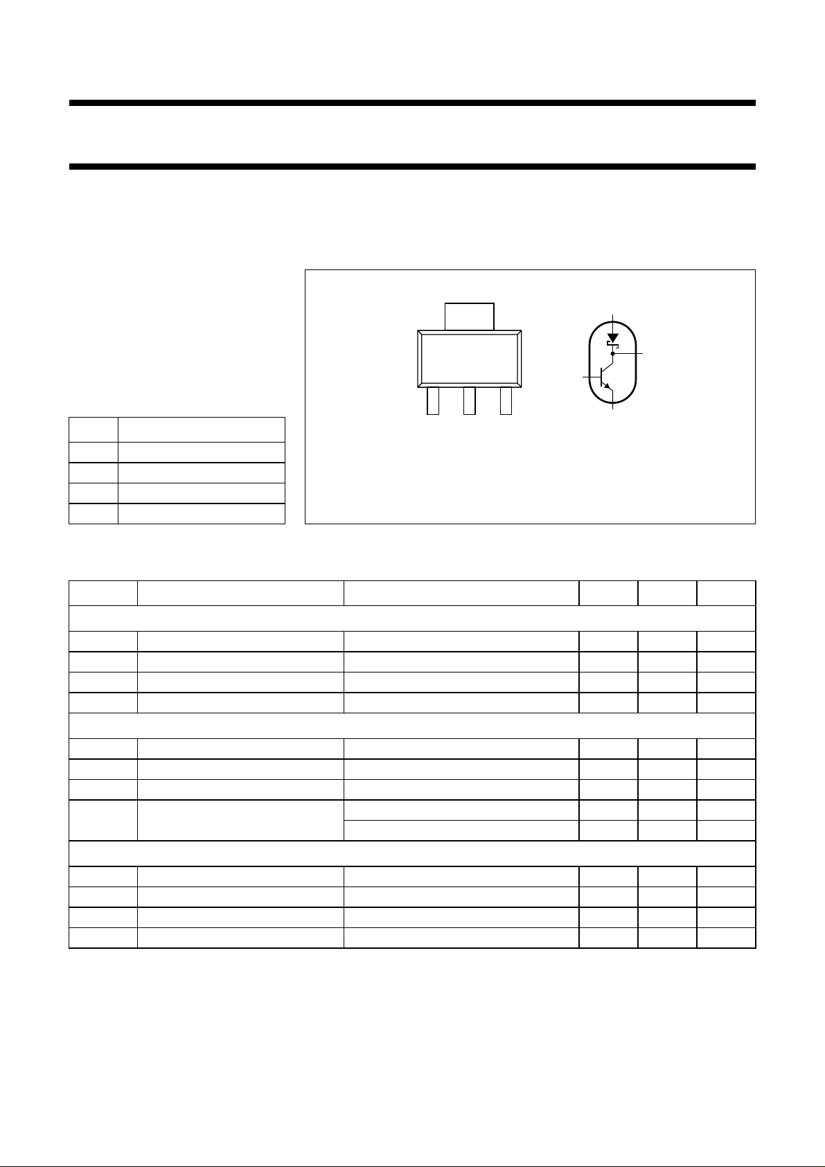
PINNING
PIN DESCRIPTION
Top view
1
2
23
MAM236
4
3
1 anode Schottky
2 base
3 emitter
4 collector, cathode Schottky
Marking code: TM1101.
Fig.1 Simplified outline (SOT223) and symbol.
LIMITING VALUES
In accordance with the Absolute Maximum Rating System (IEC 134).
SYMBOL PARAMETER CONDITIONS MIN. MAX. UNIT
NPN transistor
V
CBO
V
CES
V
EBO
I
C
collector-base voltage open emitter − 60 V
collector-emitter voltage VBE=0 − 40 V
emitter-base voltage open collector − 6V
collector current (DC) − 200 mA
Schottky barrier diode
V
R
I
F
I
F(AV)
T
j
continuous reverse voltage − 40 V
forward current (DC) − 1A
average forward current − 1A
junction temperature reverse current applied − 125 °C
Combined device
P
tot
T
amb
T
stg
T
j
total power dissipation up to T
operating ambient temperature −55 +150 °C
storage temperature −55 +150 °C
junction temperature − 150 °C
forward current applied − 150 °C
=25°C − 1.2 W
amb
1996 May 09 2
Page 3

Philips Semiconductors Product specification
NPN transistor/Schottky-diode module PZTM1101
ELECTRICAL CHARACTERISTICS
T
=25°C unless otherwise specified.
amb
SYMBOL PARAMETER CONDITIONS MIN. MAX. UNIT
NPN transistor
V
(BR)CBO
V
(BR)CES
V
(BR)EBO
I
CES
I
EBO
V
CEsat
V
CEsat
V
BEsat
V
BEsat
C
ob
C
ib
f
T
h
FE
h
FE
collector-base breakdown voltage open emitter; IC=10µA; IE=0;
collector-emitter breakdown voltage open base; IC= 1 mA; VBE=0;
emitter-base breakdown voltage open collector; IE=10µA; IC=0;
collector-emitter cut-off current VCE=20V; VBE=0 − 100 nA
emitter-base cut-off current VEB=6V; IC=0 − 50 nA
collector-emitter saturation voltage note 1
collector-emitter saturation voltage T
base-emitter saturation voltage note 1
base-emitter saturation voltage T
output capacitance IE=ie= 0; VCB=5V; f=1MHz − 4pF
input capacitance IC=ic= 0; VEB= 0.5 V; f = 1 MHz − 8pF
transition frequency IC= 10 mA; VCE= 20 V; f = 100 MHz 300 − MHz
DC current gain VCE= 1 V; note 1
DC current gain VCE=1V; T
SWITCHING TIMES (see Figs 2 and 3)
t
d
t
r
t
s
t
f
delay time VCC=5V 1 5 ns
rise time IC=50mA 1631ns
storage time Vi= 0 to 5 V 110 310 ns
fall time 70 100 ns
T
= −55 to +150 °C; note 1
amb
T
= −55 to +150 °C; note 1
amb
T
= −55 to +150 °C; note 1
amb
V
=20V; VBE= 0; T
CE
V
=6V; IC= 0; T
EB
I
= 10 mA; IB=1mA − 200 mV
C
I
= 50 mA; IB= 3.2 mA − 300 mV
C
= −55 to +150 °C; note 1
amb
I
= 10 mA; IB=1mA − 250 mV
C
I
= 50 mA; IB= 3.2 mA − 350 mV
C
I
= 10 mA; IB=1mA − 850 mV
C
I
= 50 mA; IB=5mA − 950 mV
C
= −55 to +150 °C; note 1
amb
I
= 10 mA; IB=1mA − 1000 mV
C
= 50 mA; IB=5mA − 1100 mV
I
C
I
= 0.1 mA 40 −
C
= 1 mA 70 −
I
C
I
= 10 mA 100 300
C
I
= 100 mA 30 −
C
I
= 10 mA 60 500
C
I
= 100 mA 15 −
C
amb
= −55 to +150 °C; note 1
amb
= −55 to +150 °C − 50 µA
amb
= −55 to +150 °C − 10 µA
60 − V
40 − V
6 − V
1996 May 09 3
Page 4

Philips Semiconductors Product specification
NPN transistor/Schottky-diode module PZTM1101
SYMBOL P ARAMETER CONDITIONS MIN. MAX. UNIT
Schottky barrier diode
V
F
I
R
I
R
C
j
Notes
1. Measured under pulsed conditions: tp≤ 300 µs; δ≤0.01.
2. Limiting value for Tj= 125 °C; Tj= 150 °C with reverse current applied is not allowed as this may cause thermal
runaway leading to thermal destruction of the diode. A peak junction temperature of Tj= 150 °C is only allowed with
forward voltage applied.
forward voltage IF= 100 mA; note 1 − 330 mV
I
= 100 mA; T
F
I
= 1 A; note 1 − 500 mV
F
I
= 1 A; T
F
amb
= −55 to +150 °C; note 1 − 400 mV
amb
= −55 to +150 °C; note 1 − 560 mV
reverse current VR= 40 V; note 1 − 300 µA
V
= 40 V; Tj= 125 °C;
R
T
= −55 to +150 °C; note 1
amb
− 35
(2)
mA
reverse current VR= 10 V; note 1 − 40 µA
V
= 10 V; Tj= 125 °C;
R
T
= −55 to +150 °C; note 1
amb
− 15
(2)
mA
junction capacitance VR= 0 V; f = 1 MHz − 250 pF
THERMAL CHARACTERISTICS
SYMBOL PARAMETER CONDITIONS VALUE UNIT
R
th j-a
thermal resistance from junction to ambient (combined device) note 1 100 K/W
Note
1. Refer to SOT223 standard mounting conditions.
1996 May 09 4
Page 5

Philips Semiconductors Product specification
NPN transistor/Schottky-diode module PZTM1101
GRAPHICAL DATA
handbook, halfpage
5 V
0 V
V
= 5 V DC
CC
90 Ω
(1%)
825 Ω (1%)
V
i
7.5 kΩ
(5%)
Vo (pin 4)
DUT
5.23 Ω
(1%)
Fig.2 Switching times test circuit.
MBH220
handbook, halfpage
INPUT
V
i
t
p
V
o
OUTPUT
tr< 5ns (10% to 90%); tp=1µs; δ = 0.02; Zi=50Ω.
ton=td+tr; t
10% 90%
90%
t
d
off=ts+tf
t
r
t
on
.
10%
Fig.3 Input and output waveforms.
5 V
0 V
t
t
s
t
off
f
MBH221
1996 May 09 5
Page 6

Philips Semiconductors Product specification
NPN transistor/Schottky-diode module PZTM1101
PACKAGE OUTLINE
handbook, full pagewidth
Dimensions in mm.
16
max
0.95
0.85
6.7
6.3
3.1
2.9
4.6
0.80
0.60
0.1 S
4
B
A
3.7
3.3
0.1 B
(4x)
M
0.2 A
7.3
6.7
M
MSA035 - 1
o
S seating plane
123
2.3
0.32
0.24
0.10
0.01
o
1.80
max
16
10
max
o
Fig.4 SOT223.
1996 May 09 6
Page 7

Philips Semiconductors Product specification
NPN transistor/Schottky-diode module PZTM1101
DEFINITIONS
Data sheet status
Objective specification This data sheet contains target or goal specifications for product development.
Preliminary specification This data sheet contains preliminary data; supplementary data may be published later.
Product specification This data sheet contains final product specifications.
Limiting values
Limiting values given are in accordance with the Absolute Maximum Rating System (IEC 134). Stress above one or
more of the limiting values may cause permanent damage to the device. These are stress ratings only and operation
of the device at these or at any other conditions above those given in the Characteristics sections of the specification
is not implied. Exposure to limiting values for extended periods may affect device reliability.
Application information
Where application information is given, it is advisory and does not form part of the specification.
LIFE SUPPORT APPLICATIONS
These products are not designed for use in life support appliances, devices, or systems where malfunction of these
products can reasonably be expected to result in personal injury. Philips customers using or selling these products for
use in such applications do so at their own risk and agree to fully indemnify Philips for any damages resulting from such
improper use or sale.
1996 May 09 7
 Loading...