

Datasheet X-NUCLEO-6180XA1, P-NUCLEO-6180X1, P-NUCLEO-6180X2 Datasheet (STMicroelectronics)
Page 1
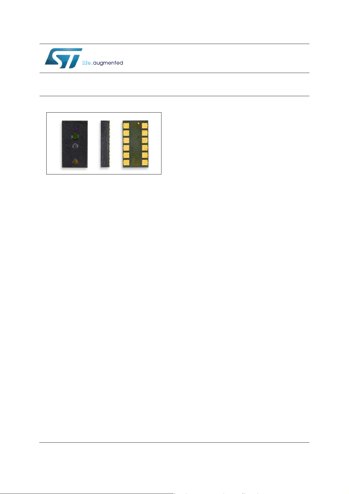
VL6180X
Proximity and ambient light sensing (ALS) module
Datasheet - production data
• Two programmable GPIO
– Window and thresholding functions for both
ranging and ALS
Description
Features
• Three-in-one smart optical module
– Proximity sensor
– Ambient Light Sensor
– VCSEL light source
• Fast, accurate distance ranging
– Measures absolute range from 0 to above
10 cm
– Independent of object reflectance
– Ambient rejection
– Crosstalk compensation for cover glass
– Ranging beyond 100mm is possible with
certain target reflectances and ambient
conditions but not guaranteed
• Gesture recognition
– Distance and signal level can be used by
host system to implement gesture
recognition
– Demo systems available.
• Ambient light sensor
– High dynamic range
– Accurate/sensitive in ultra-low light
– Calibrated output value in lux
• Easy integration
– Single reflowable component
– No additional optics or gasket
– Single power supply
2
–I
C interface for device control and data
The VL6180X is the latest product based on ST’s
patented FlightSense
ground-breaking technology allowing absolute
distance to be measured independent of target
reflectance. Instead of estimating the distance by
measuring the amount of light reflected back from
the object (which is significantly influenced by
color and surface), the VL6180X precisely
measures the time the light takes to travel to the
nearest object and reflect back to the sensor
(Time-of-Flight).
Combining an IR emitter, a range sensor and an
ambient light sensor in a three-in-one ready-touse reflowable package, the VL6180X is easy to
integrate and saves the end-product maker long
and costly optical and mechanical design
optimizations.
The module is designed for ultra low power
operation. Ranging and ALS measurements can
be automatically performed at user defined
intervals. Multiple threshold and interrupt
schemes are supported to minimize host
operations.
Host control and result reading is performed using
2
an I
C interface. Optional additional functions,
such as measurement ready and threshold
interrupts, are provided by two prog ra m m ab l e
GPIO pins.
™
technology. This is a
Applications
• Smartphones/portable touchscreen devices
• Tablet/laptop/gaming devices
• Domestic appliances/industrial devices
August 2014 DocID026171 Rev 6 1/79
This is information on a product in full production.
www.st.com
Page 2

Contents VL6180X
Contents
1 Overview . . . . . . . . . . . . . . . . . . . . . . . . . . . . . . . . . . . . . . . . . . . . . . . . . . 8
1.1 Technical specification . . . . . . . . . . . . . . . . . . . . . . . . . . . . . . . . . . . . . . . . 8
1.2 System block diagram . . . . . . . . . . . . . . . . . . . . . . . . . . . . . . . . . . . . . . . . 9
1.3 Device pinout . . . . . . . . . . . . . . . . . . . . . . . . . . . . . . . . . . . . . . . . . . . . . . . 9
1.4 Application schematic . . . . . . . . . . . . . . . . . . . . . . . . . . . . . . . . . . . . . . . . 10
1.5 Recommended solder pad dimensions . . . . . . . . . . . . . . . . . . . . . . . . . . .11
1.6 Recommended reflow profile . . . . . . . . . . . . . . . . . . . . . . . . . . . . . . . . . . .11
2 Functional description . . . . . . . . . . . . . . . . . . . . . . . . . . . . . . . . . . . . . . 12
2.1 System state diagram . . . . . . . . . . . . . . . . . . . . . . . . . . . . . . . . . . . . . . . . 13
2.2 Timing diagram . . . . . . . . . . . . . . . . . . . . . . . . . . . . . . . . . . . . . . . . . . . . . 14
2.3 Software overview . . . . . . . . . . . . . . . . . . . . . . . . . . . . . . . . . . . . . . . . . . 15
2.4 Operating modes . . . . . . . . . . . . . . . . . . . . . . . . . . . . . . . . . . . . . . . . . . . 16
2.4.1 Single-shot range/ALS operation . . . . . . . . . . . . . . . . . . . . . . . . . . . . . . 17
2.4.2 Continuous range/ALS operation . . . . . . . . . . . . . . . . . . . . . . . . . . . . . . 17
2.4.3 Interleaved mode . . . . . . . . . . . . . . . . . . . . . . . . . . . . . . . . . . . . . . . . . . 18
2.4.4 Continuous mode limits . . . . . . . . . . . . . . . . . . . . . . . . . . . . . . . . . . . . . 18
2.5 Range timing . . . . . . . . . . . . . . . . . . . . . . . . . . . . . . . . . . . . . . . . . . . . . . 19
2.6 Interrupt modes . . . . . . . . . . . . . . . . . . . . . . . . . . . . . . . . . . . . . . . . . . . . 20
2.7 Range error codes . . . . . . . . . . . . . . . . . . . . . . . . . . . . . . . . . . . . . . . . . . 20
2.8 Range checks . . . . . . . . . . . . . . . . . . . . . . . . . . . . . . . . . . . . . . . . . . . . . . 21
2.8.1 Early convergence estimate (ECE) . . . . . . . . . . . . . . . . . . . . . . . . . . . . 21
2.8.2 Range ignore . . . . . . . . . . . . . . . . . . . . . . . . . . . . . . . . . . . . . . . . . . . . . 22
2.8.3 Signal-to-noise ratio (SNR) . . . . . . . . . . . . . . . . . . . . . . . . . . . . . . . . . . 23
2.9 Manual/autoVHV calibration . . . . . . . . . . . . . . . . . . . . . . . . . . . . . . . . . . . 23
2.10 History buffer . . . . . . . . . . . . . . . . . . . . . . . . . . . . . . . . . . . . . . . . . . . . . . 23
2.11 Current consumption . . . . . . . . . . . . . . . . . . . . . . . . . . . . . . . . . . . . . . . . 24
2.11.1 Ranging current consumption . . . . . . . . . . . . . . . . . . . . . . . . . . . . . . . . 24
2.11.2 Current consumption calculator . . . . . . . . . . . . . . . . . . . . . . . . . . . . . . . 25
2.11.3 Current distribution . . . . . . . . . . . . . . . . . . . . . . . . . . . . . . . . . . . . . . . . 26
2.12 Other system considerations . . . . . . . . . . . . . . . . . . . . . . . . . . . . . . . . . . 27
2.12.1 Part-to-part range offset . . . . . . . . . . . . . . . . . . . . . . . . . . . . . . . . . . . . . 27
2/79 DocID026171 Rev 6
Page 3

VL6180X Contents
2.12.2 Cross-talk . . . . . . . . . . . . . . . . . . . . . . . . . . . . . . . . . . . . . . . . . . . . . . . . 27
2.12.3 Offset calibration procedure . . . . . . . . . . . . . . . . . . . . . . . . . . . . . . . . . . 27
2.12.4 Cross-talk calibration procedure . . . . . . . . . . . . . . . . . . . . . . . . . . . . . . 28
2.12.5 Cross-talk limit . . . . . . . . . . . . . . . . . . . . . . . . . . . . . . . . . . . . . . . . . . . . 29
2.12.6 Cross-talk vs air gap . . . . . . . . . . . . . . . . . . . . . . . . . . . . . . . . . . . . . . . 29
2.13 Ambient light sensor (ALS) . . . . . . . . . . . . . . . . . . . . . . . . . . . . . . . . . . . . 30
2.13.1 Field of view . . . . . . . . . . . . . . . . . . . . . . . . . . . . . . . . . . . . . . . . . . . . . . 30
2.13.2 Spectral response . . . . . . . . . . . . . . . . . . . . . . . . . . . . . . . . . . . . . . . . . 30
2.13.3 ALS dynamic range . . . . . . . . . . . . . . . . . . . . . . . . . . . . . . . . . . . . . . . . 31
2.13.4 ALS count to lux conversion . . . . . . . . . . . . . . . . . . . . . . . . . . . . . . . . . 31
2.13.5 Integration period . . . . . . . . . . . . . . . . . . . . . . . . . . . . . . . . . . . . . . . . . . 32
2.13.6 ALS gain selection . . . . . . . . . . . . . . . . . . . . . . . . . . . . . . . . . . . . . . . . . 32
3 Electrical characteristics . . . . . . . . . . . . . . . . . . . . . . . . . . . . . . . . . . . . 33
3.1 Absolute maximum ratings . . . . . . . . . . . . . . . . . . . . . . . . . . . . . . . . . . . . 33
3.2 Normal operating conditions . . . . . . . . . . . . . . . . . . . . . . . . . . . . . . . . . . . 33
3.3 Current consumption . . . . . . . . . . . . . . . . . . . . . . . . . . . . . . . . . . . . . . . . 33
3.4 Electrical characteristics . . . . . . . . . . . . . . . . . . . . . . . . . . . . . . . . . . . . . . 34
4 Performance specification . . . . . . . . . . . . . . . . . . . . . . . . . . . . . . . . . . . 35
4.1 Proximity ranging (0 to 100mm) . . . . . . . . . . . . . . . . . . . . . . . . . . . . . . . . 35
4.1.1 Max range vs. ambient light level . . . . . . . . . . . . . . . . . . . . . . . . . . . . . 35
4.2 ALS performance . . . . . . . . . . . . . . . . . . . . . . . . . . . . . . . . . . . . . . . . . . . 36
5I
2
C control interface . . . . . . . . . . . . . . . . . . . . . . . . . . . . . . . . . . . . . . . . 37
6 Device registers . . . . . . . . . . . . . . . . . . . . . . . . . . . . . . . . . . . . . . . . . . . . 40
6.1 Register encoding formats . . . . . . . . . . . . . . . . . . . . . . . . . . . . . . . . . . . . 40
6.2 Register descriptions . . . . . . . . . . . . . . . . . . . . . . . . . . . . . . . . . . . . . . . . 43
6.2.1 IDENTIFICATION__MODEL_ID . . . . . . . . . . . . . . . . . . . . . . . . . . . . . . 43
6.2.2 IDENTIFICATION__MODEL_REV_MAJOR . . . . . . . . . . . . . . . . . . . . . 43
6.2.3 IDENTIFICATION__MODEL_REV_MINOR . . . . . . . . . . . . . . . . . . . . . 43
6.2.4 IDENTIFICATION__MODULE_REV_MAJOR . . . . . . . . . . . . . . . . . . . . 44
6.2.5 IDENTIFICATION__MODULE_REV_MINOR . . . . . . . . . . . . . . . . . . . . 44
6.2.6 IDENTIFICATION__DATE_HI . . . . . . . . . . . . . . . . . . . . . . . . . . . . . . . . 44
6.2.7 IDENTIFICATION__DATE_LO . . . . . . . . . . . . . . . . . . . . . . . . . . . . . . . 45
DocID026171 Rev 6 3/79
5
Page 4

Contents VL6180X
6.2.8 IDENTIFICATION__TIME . . . . . . . . . . . . . . . . . . . . . . . . . . . . . . . . . . . 45
6.2.9 SYSTEM__MODE_GPIO0 . . . . . . . . . . . . . . . . . . . . . . . . . . . . . . . . . . 46
6.2.10 SYSTEM__MODE_GPIO1 . . . . . . . . . . . . . . . . . . . . . . . . . . . . . . . . . . 47
6.2.11 SYSTEM__HISTORY_CTRL . . . . . . . . . . . . . . . . . . . . . . . . . . . . . . . . . 48
6.2.12 SYSTEM__INTERRUPT_CONFIG_GPIO . . . . . . . . . . . . . . . . . . . . . . 49
6.2.13 SYSTEM__INTERRUPT_CLEAR . . . . . . . . . . . . . . . . . . . . . . . . . . . . . 49
6.2.14 SYSTEM__FRESH_OUT_OF_RESET . . . . . . . . . . . . . . . . . . . . . . . . . 50
6.2.15 SYSTEM__GROUPED_PARAMETER_HOLD . . . . . . . . . . . . . . . . . . . 50
6.2.16 SYSRANGE__START . . . . . . . . . . . . . . . . . . . . . . . . . . . . . . . . . . . . . . 51
6.2.17 SYSRANGE__THRESH_HIGH . . . . . . . . . . . . . . . . . . . . . . . . . . . . . . . 51
6.2.18 SYSRANGE__THRESH_LOW . . . . . . . . . . . . . . . . . . . . . . . . . . . . . . . 52
6.2.19 SYSRANGE__INTERMEASUREMENT_PERIOD . . . . . . . . . . . . . . . . 52
6.2.20 SYSRANGE__MAX_CONVERGENCE_TIME . . . . . . . . . . . . . . . . . . . 52
6.2.21 SYSRANGE__CROSSTALK_COMPENSATION_RATE . . . . . . . . . . . . 53
6.2.22 SYSRANGE__CROSSTALK_VALID_HEIGHT . . . . . . . . . . . . . . . . . . . 53
6.2.23 SYSRANGE__EARLY_CONVERGENCE_ESTIMATE . . . . . . . . . . . . . 53
6.2.24 SYSRANGE__PART_TO_PART_RANGE_OFFSET . . . . . . . . . . . . . . 54
6.2.25 SYSRANGE__RANGE_IGNORE_VALID_HEIGHT . . . . . . . . . . . . . . . 54
6.2.26 SYSRANGE__RANGE_IGNORE_THRESHOLD . . . . . . . . . . . . . . . . . 54
6.2.27 SYSRANGE__MAX_AMBIENT_LEVEL_MULT . . . . . . . . . . . . . . . . . . 55
6.2.28 SYSRANGE__RANGE_CHECK_ENABLES . . . . . . . . . . . . . . . . . . . . . 55
6.2.29 SYSRANGE__VHV_RECALIBRATE . . . . . . . . . . . . . . . . . . . . . . . . . . . 56
6.2.30 SYSRANGE__VHV_REPEAT_RATE . . . . . . . . . . . . . . . . . . . . . . . . . . 56
6.2.31 SYSALS__START . . . . . . . . . . . . . . . . . . . . . . . . . . . . . . . . . . . . . . . . . 57
6.2.32 SYSALS__THRESH_HIGH . . . . . . . . . . . . . . . . . . . . . . . . . . . . . . . . . . 57
6.2.33 SYSALS__THRESH_LOW . . . . . . . . . . . . . . . . . . . . . . . . . . . . . . . . . . 58
6.2.34 SYSALS__INTERMEASUREMENT_PERIOD . . . . . . . . . . . . . . . . . . . 58
6.2.35 SYSALS__ANALOGUE_GAIN . . . . . . . . . . . . . . . . . . . . . . . . . . . . . . . 59
6.2.36 SYSALS__INTEGRATION_PERIOD . . . . . . . . . . . . . . . . . . . . . . . . . . . 59
6.2.37 RESULT__RANGE_STATUS . . . . . . . . . . . . . . . . . . . . . . . . . . . . . . . . 60
6.2.38 RESULT__ALS_STATUS . . . . . . . . . . . . . . . . . . . . . . . . . . . . . . . . . . . 61
6.2.39 RESULT__INTERRUPT_STATUS_GPIO . . . . . . . . . . . . . . . . . . . . . . . 62
6.2.40 RESULT__ALS_V AL . . . . . . . . . . . . . . . . . . . . . . . . . . . . . . . . . . . . . . . 62
6.2.41 RESULT__HISTORY_BUFFER_x . . . . . . . . . . . . . . . . . . . . . . . . . . . . . 63
6.2.42 RESULT__RANGE_VAL . . . . . . . . . . . . . . . . . . . . . . . . . . . . . . . . . . . . 64
6.2.43 RESULT__RANGE_RAW . . . . . . . . . . . . . . . . . . . . . . . . . . . . . . . . . . . 64
6.2.44 RESULT__RANGE_RETURN_RATE . . . . . . . . . . . . . . . . . . . . . . . . . . 64
4/79 DocID026171 Rev 6
Page 5

VL6180X Contents
6.2.45 RESULT__RANGE_REFERENCE_RATE . . . . . . . . . . . . . . . . . . . . . . . 65
6.2.46 RESULT__RANGE_RETURN_SIGNAL_COUNT . . . . . . . . . . . . . . . . . 65
6.2.47 RESULT__RANGE_REFERENCE_SIGNAL_COUNT . . . . . . . . . . . . . 66
6.2.48 RESULT__RANGE_RETURN_AMB_COUNT . . . . . . . . . . . . . . . . . . . . 66
6.2.49 RESULT__RANGE_REFERENCE_AMB_COUNT . . . . . . . . . . . . . . . . 66
6.2.50 RESULT__RANGE_RETURN_CONV_TIME . . . . . . . . . . . . . . . . . . . . 67
6.2.51 RESULT__RANGE_REFERENCE_CONV_TIME . . . . . . . . . . . . . . . . . 67
6.2.52 READOUT__AVERAGING_SAMPLE_PERIOD . . . . . . . . . . . . . . . . . . 67
6.2.53 FIRMWARE__BOOTUP . . . . . . . . . . . . . . . . . . . . . . . . . . . . . . . . . . . . 68
6.2.54 FIRMWARE__RESULT_SCALER . . . . . . . . . . . . . . . . . . . . . . . . . . . . . 68
6.2.55 I2C_SLAVE__DEVICE_ADDRESS . . . . . . . . . . . . . . . . . . . . . . . . . . . . 68
6.2.56 INTERLEAVED_MODE__ENABLE . . . . . . . . . . . . . . . . . . . . . . . . . . . . 69
7 Outline drawing . . . . . . . . . . . . . . . . . . . . . . . . . . . . . . . . . . . . . . . . . . . . 70
8 Laser safety considerations . . . . . . . . . . . . . . . . . . . . . . . . . . . . . . . . . . 72
8.1 Compliance . . . . . . . . . . . . . . . . . . . . . . . . . . . . . . . . . . . . . . . . . . . . . . . 72
9 Ordering information . . . . . . . . . . . . . . . . . . . . . . . . . . . . . . . . . . . . . . . 73
9.1 Traceability and identification . . . . . . . . . . . . . . . . . . . . . . . . . . . . . . . . . . 73
9.2 Part marking . . . . . . . . . . . . . . . . . . . . . . . . . . . . . . . . . . . . . . . . . . . . . . . 73
9.3 Packaging . . . . . . . . . . . . . . . . . . . . . . . . . . . . . . . . . . . . . . . . . . . . . . . . 74
9.3.1 Package labeling . . . . . . . . . . . . . . . . . . . . . . . . . . . . . . . . . . . . . . . . . . 74
9.4 Storage . . . . . . . . . . . . . . . . . . . . . . . . . . . . . . . . . . . . . . . . . . . . . . . . . . . 75
9.5 ROHS compliance . . . . . . . . . . . . . . . . . . . . . . . . . . . . . . . . . . . . . . . . . . 75
10 ECOPACK
® . . . . . . . . . . . . . . . . . . . . . . . . . . . . . . . . . . . . . . . . . . . . . . . . . . . . . . . . . . . . 76
11 Revision history . . . . . . . . . . . . . . . . . . . . . . . . . . . . . . . . . . . . . . . . . . . 77
DocID026171 Rev 6 5/79
5
Page 6

List of tables VL6180X
List of tables
Table 1. Technical specification . . . . . . . . . . . . . . . . . . . . . . . . . . . . . . . . . . . . . . . . . . . . . . . . . . . . . 8
Table 2. VL6180X pin numbers and signal descriptions. . . . . . . . . . . . . . . . . . . . . . . . . . . . . . . . . . 10
Table 3. Recommended reflow profile . . . . . . . . . . . . . . . . . . . . . . . . . . . . . . . . . . . . . . . . . . . . . . . 11
Table 4. Power-up timing constraints . . . . . . . . . . . . . . . . . . . . . . . . . . . . . . . . . . . . . . . . . . . . . . . . 14
Table 5. Operating modes . . . . . . . . . . . . . . . . . . . . . . . . . . . . . . . . . . . . . . . . . . . . . . . . . . . . . . . . 16
Table 6. Inte rle av ed mo de limits (1 0 Hz op eration) . . . . . . . . . . . . . . . . . . . . . . . . . . . . . . . . . . . . . 19
Table 7. Typical range convergence time (ms). . . . . . . . . . . . . . . . . . . . . . . . . . . . . . . . . . . . . . . . . 20
Table 8. Range error codes . . . . . . . . . . . . . . . . . . . . . . . . . . . . . . . . . . . . . . . . . . . . . . . . . . . . . . . 21
Table 9. History buffer . . . . . . . . . . . . . . . . . . . . . . . . . . . . . . . . . . . . . . . . . . . . . . . . . . . . . . . . . . . 24
Table 10. Typical current consumption in different operating states . . . . . . . . . . . . . . . . . . . . . . . . . 24
Table 11. Breakdown of current consumption . . . . . . . . . . . . . . . . . . . . . . . . . . . . . . . . . . . . . . . . . . 25
Table 12. Current consumption on AVDD and AVDD_VCSEL. . . . . . . . . . . . . . . . . . . . . . . . . . . . . . 26
Table 13. ALS dynamic range . . . . . . . . . . . . . . . . . . . . . . . . . . . . . . . . . . . . . . . . . . . . . . . . . . . . . . 31
Table 14. Actual gain values. . . . . . . . . . . . . . . . . . . . . . . . . . . . . . . . . . . . . . . . . . . . . . . . . . . . . . . . 32
Table 15. Absolute maximum ratings . . . . . . . . . . . . . . . . . . . . . . . . . . . . . . . . . . . . . . . . . . . . . . . . . 33
Table 16. Normal operating conditions. . . . . . . . . . . . . . . . . . . . . . . . . . . . . . . . . . . . . . . . . . . . . . . . 33
Table 17. Current consumption . . . . . . . . . . . . . . . . . . . . . . . . . . . . . . . . . . . . . . . . . . . . . . . . . . . . . 33
Table 18. Digital I/O electrical characteristics. . . . . . . . . . . . . . . . . . . . . . . . . . . . . . . . . . . . . . . . . . . 34
Table 19. Ranging specification . . . . . . . . . . . . . . . . . . . . . . . . . . . . . . . . . . . . . . . . . . . . . . . . . . . . . 35
Table 20. Worst case max range vs. ambient 0 to 100mm . . . . . . . . . . . . . . . . . . . . . . . . . . . . . . . . 35
Table 21. ALS performance . . . . . . . . . . . . . . . . . . . . . . . . . . . . . . . . . . . . . . . . . . . . . . . . . . . . . . . . 36
Table 22. Register groups . . . . . . . . . . . . . . . . . . . . . . . . . . . . . . . . . . . . . . . . . . . . . . . . . . . . . . . . . 40
Table 23. 32-bit register example . . . . . . . . . . . . . . . . . . . . . . . . . . . . . . . . . . . . . . . . . . . . . . . . . . . . 40
Table 24. 9.7 and 4.4 register formats . . . . . . . . . . . . . . . . . . . . . . . . . . . . . . . . . . . . . . . . . . . . . . . . 40
Table 25. Register summary. . . . . . . . . . . . . . . . . . . . . . . . . . . . . . . . . . . . . . . . . . . . . . . . . . . . . . . . 41
Table 26. Delivery format . . . . . . . . . . . . . . . . . . . . . . . . . . . . . . . . . . . . . . . . . . . . . . . . . . . . . . . . . . 73
Table 27. Storage conditions . . . . . . . . . . . . . . . . . . . . . . . . . . . . . . . . . . . . . . . . . . . . . . . . . . . . . . . 75
Table 28. Document revision history . . . . . . . . . . . . . . . . . . . . . . . . . . . . . . . . . . . . . . . . . . . . . . . . . 77
6/79 DocID026171 Rev 6
Page 7

VL6180X List of figures
List of figures
Figure 1. VL6180X block diagram . . . . . . . . . . . . . . . . . . . . . . . . . . . . . . . . . . . . . . . . . . . . . . . . . . . . 9
Figure 2. VL6180X pinout . . . . . . . . . . . . . . . . . . . . . . . . . . . . . . . . . . . . . . . . . . . . . . . . . . . . . . . . . . 9
Figure 3. Root part number 1 schematic . . . . . . . . . . . . . . . . . . . . . . . . . . . . . . . . . . . . . . . . . . . . . . 10
Figure 4. Recommended solder pattern . . . . . . . . . . . . . . . . . . . . . . . . . . . . . . . . . . . . . . . . . . . . . . 11
Figure 5. Recommended reflow profile . . . . . . . . . . . . . . . . . . . . . . . . . . . . . . . . . . . . . . . . . . . . . . . 11
Figure 6. Typical ranging performance . . . . . . . . . . . . . . . . . . . . . . . . . . . . . . . . . . . . . . . . . . . . . . . 12
Figure 7. ALS linearity . . . . . . . . . . . . . . . . . . . . . . . . . . . . . . . . . . . . . . . . . . . . . . . . . . . . . . . . . . . . 12
Figure 8. System state diagram. . . . . . . . . . . . . . . . . . . . . . . . . . . . . . . . . . . . . . . . . . . . . . . . . . . . . 13
Figure 9. Power-up timing . . . . . . . . . . . . . . . . . . . . . . . . . . . . . . . . . . . . . . . . . . . . . . . . . . . . . . . . . 14
Figure 10. Software overview . . . . . . . . . . . . . . . . . . . . . . . . . . . . . . . . . . . . . . . . . . . . . . . . . . . . . . . 15
Figure 11. Interleaved mode . . . . . . . . . . . . . . . . . . . . . . . . . . . . . . . . . . . . . . . . . . . . . . . . . . . . . . . . 18
Figure 12. Total range execution time . . . . . . . . . . . . . . . . . . . . . . . . . . . . . . . . . . . . . . . . . . . . . . . . . 19
Figure 13. Early convergence estimate (ECE). . . . . . . . . . . . . . . . . . . . . . . . . . . . . . . . . . . . . . . . . . . 22
Figure 14. Typical ranging current consumption (10 Hz sampling rate). . . . . . . . . . . . . . . . . . . . . . . . 25
Figure 15. VCSEL pulse duty cycle . . . . . . . . . . . . . . . . . . . . . . . . . . . . . . . . . . . . . . . . . . . . . . . . . . . 26
Figure 16. Part-to-part range offset . . . . . . . . . . . . . . . . . . . . . . . . . . . . . . . . . . . . . . . . . . . . . . . . . . . 27
Figure 17. Cross-talk compensation . . . . . . . . . . . . . . . . . . . . . . . . . . . . . . . . . . . . . . . . . . . . . . . . . . 27
Figure 18. Cross-talk vs air gap. . . . . . . . . . . . . . . . . . . . . . . . . . . . . . . . . . . . . . . . . . . . . . . . . . . . . . 29
Figure 19. ALS angular response . . . . . . . . . . . . . . . . . . . . . . . . . . . . . . . . . . . . . . . . . . . . . . . . . . . . 30
Figure 20. ALS spectral response . . . . . . . . . . . . . . . . . . . . . . . . . . . . . . . . . . . . . . . . . . . . . . . . . . . . 30
Figure 21. Serial interface data transfer protocol. . . . . . . . . . . . . . . . . . . . . . . . . . . . . . . . . . . . . . . . . 37
Figure 22. I2C device address. . . . . . . . . . . . . . . . . . . . . . . . . . . . . . . . . . . . . . . . . . . . . . . . . . . . . . . 37
Figure 23. Single location, single write) . . . . . . . . . . . . . . . . . . . . . . . . . . . . . . . . . . . . . . . . . . . . . . . . 37
Figure 24. Single location, single read. . . . . . . . . . . . . . . . . . . . . . . . . . . . . . . . . . . . . . . . . . . . . . . . . 38
Figure 25. Multiple location write . . . . . . . . . . . . . . . . . . . . . . . . . . . . . . . . . . . . . . . . . . . . . . . . . . . . . 38
Figure 26. Multiple location read . . . . . . . . . . . . . . . . . . . . . . . . . . . . . . . . . . . . . . . . . . . . . . . . . . . . . 39
Figure 27. Outline drawing (page 1/2) . . . . . . . . . . . . . . . . . . . . . . . . . . . . . . . . . . . . . . . . . . . . . . . . . 70
Figure 28. Outline drawing (page 2/2) . . . . . . . . . . . . . . . . . . . . . . . . . . . . . . . . . . . . . . . . . . . . . . . . . 71
Figure 29. Class 1 laser product label . . . . . . . . . . . . . . . . . . . . . . . . . . . . . . . . . . . . . . . . . . . . . . . . . 72
Figure 30. Part marking . . . . . . . . . . . . . . . . . . . . . . . . . . . . . . . . . . . . . . . . . . . . . . . . . . . . . . . . . . . . 73
Figure 31. Tape and reel packaging . . . . . . . . . . . . . . . . . . . . . . . . . . . . . . . . . . . . . . . . . . . . . . . . . . 74
Figure 32. Package labeling . . . . . . . . . . . . . . . . . . . . . . . . . . . . . . . . . . . . . . . . . . . . . . . . . . . . . . . . 74
DocID026171 Rev 6 7/79
7
Page 8
Overview VL6180X
1 Overview
This datasheet is applicable to the final VL6180X ROM code revision.
1.1 Technical specification
Table 1. Technical specification
Feature Detail
Package Optical LGA12
Size 4.8 x 2.8 x 1.0 mm
Ranging 0 to 100 mm
< 1 Lux up to 100 kLux
Ambient light sensor
16-bit output
(1)
(3)
(2)
8 manual gain settings
Operating voltage:
• Functional range
• Op timum range
(4)
2.6 to 3.0 V
2.7 to 2.9 V
Operating temperature:
• Functional range
• Op timum range
(4)
-20 to 70°C
-10 to 60°C
Hardware standby (GPIO0 = 0): < 1 μA
Typical power consumption
Software standby: < 1 μA
ALS: 300 μA
Ranging: 1.7 mA (typical average)
(5)
IR emitter 850 nm
2
C
I
1. Ranging beyond 100 mm is possible with certain target reflectances and ambient conditions but not
guaranteed
2. When used under a cover glass with 10% transmission in the visible spectrum
3. Digital output easily converted to Lux
4. Please refer to Table 19.: Ranging specification
5. Assumes 10 Hz sampling rate, 17% reflective target at 50 mm
400 kHz serial bus
Address: 0x29 (7-bit)
8/79 DocID026171 Rev 6
Page 9
VL6180X Overview
VL6180X module
VL6180X silicon
Ranging ALS
Microcontroller
NVM RAM
IR emitter driver
IR- IR+
IR emitter
GPIO-0
GPIO-1
SDA
SCL
AVDD
AVDD_VCSEL
AVSS
AVSS_VCSEL
VL6180X
1
6
7
12
GPIO1
NC
NC
SCL
SDA
GPIO0
AVSS
AVDD
NC
AVDD_VCSEL
NC
AVSS_VCSEL
2
3
4
5
8
9
10
11
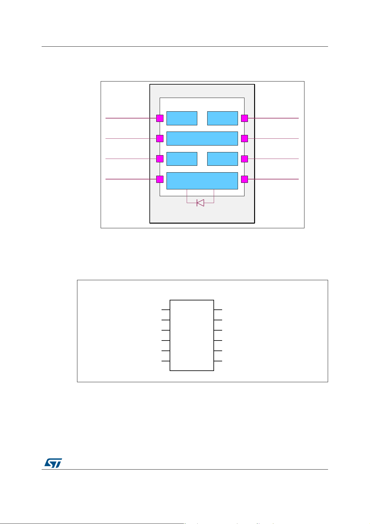
1.2 System block diagram
Figure 1. VL6180X block diagram
1.3 Device pinout
Figure 2 shows the pinout of the VL6180X.
Figure 2. VL6180X pinout
DocID026171 Rev 6 9/79
78
Page 10
Overview VL6180X
VL6180X
1
6
7
12
GPIO1
NC
NC
(3)
SCL
SDA
GPIO0
AVSS
AVDD
NC
AVDD_VCSEL
NC
AVSS_VCSEL
3
4
5
8
9
10
112
2.8V
1.8V or 2.8V
GPIO1
(1)
GPIO0
(1)
SCL
(2)
SDA
(2)
4.7 uF
100 nF
Table 2. VL6180X pin numbers and signal descriptions
Pin number Signal name Signal type Signal description
1 GPIO1 Digital I/O Interrupt output. Open-drain.
2 NC No connect or ground
3 NC No connect or ground
Power-up default is chip enable
4 GPIO0/CE Digital I/O
(CE). It should be pulled high with a
47 kΩ resistor.
5 SCL Digital input I
6 SDA Digital I/O I
2
C serial clock
2
C serial data
7 NC No connect or ground
8 AVDD_VCSEL Supply VCSEL power supply. 2.6 to 3.0 V
9 AVSS_VCSEL Ground VCSEL ground
10 AVDD Supply
Digital/analog po w er su pp l y. 2.6 to
3.0 V
11 NC No connect or ground
12 AVSS Ground Digital/analog ground
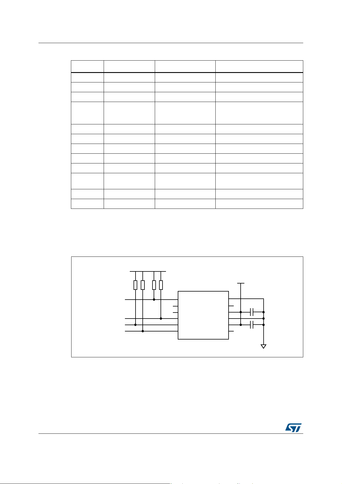
1.4 Application schematic
Figure 3 shows the schematic of the VL6180X.
Figure 3. Root part number 1 schematic
1. Open drain. Recommend 47 kΩ
2. Open drain. Pull up resistors typically fitted once per I2C bus at host
3. No connects can also be grounded if required
Note: Capacitors on AVDD and AVDD_VCSEL should be placed as close as possible to the
supply pads.
10/79 DocID026171 Rev 6
Page 11
VL6180X Overview
0.55 mm
0.60 mm
Pad pitch 0.75 mm
1.40 mm
Same as device pad dimensions
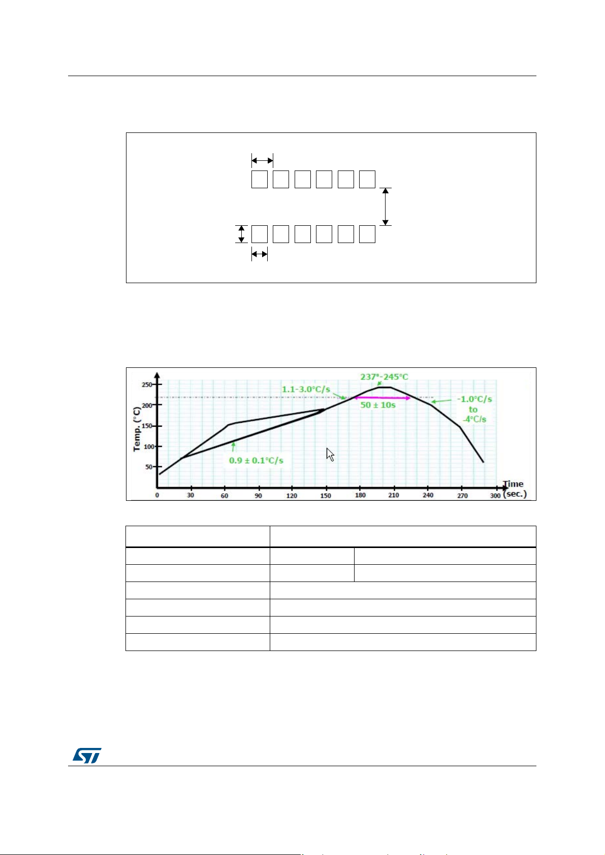
1.5 Recommended solder pad dimensions
Figure 4. Recommended solder pattern
1.6 Recommended reflow profile
The recommend reflow profile is shown in Figure 5 and Table 3.
Figure 5. Recommended reflow profile
Profile Ramp to strike
Temperature gradient in preheat (T= 70 - 180°C): 0.9 +/- 0.1°C/s
Temperature gradient (T= 200 - 225°C): 1.1 - 3.0°C/s
Peak temperature in reflow 237°C - 245°C
Time above 220°C 50 +/- 10 seconds
Temperature gradient in cooling -1 to -4 °C/s (-6°C/s maximum)
Time from 50 to 220°C 160 to 220 seconds
Table 3. Recommended reflow profile
Note: As the VL6180X package is not sealed, only a dry re-flow process should be used (such as
convection re-flow). Vapor phase re-flow is not suitable for this type of optical component.
The VL6180X is an optical component and as such, it should be treated carefully. This
would typically include using a ‘no-wash’ assembly process.
DocID026171 Rev 6 11/79
78
Page 12
Functional description VL6180X
ϭϬ
ϭϬϬ
ϭϬϬϬ
ϭϬϬϬϬ
ϭϬϬϬϬϬ
ϭ ϭϬ ϭϬϬ ϭϬϬϬ ϭϬϬϬϬ
Z^h>dͺͺ>^ͺs>
>ŝŐŚƚůĞǀĞů;>ƵdžͿ
'ĂŝŶϭ
'ĂŝŶϭϮϱ
'ĂŝŶϭϲϳ
'ĂŝŶϮϱ
'ĂŝŶϱ
'ĂŝŶϭϬ
'ĂŝŶϮϬ
'ĂŝŶϰϬ
^ĂƚƵƌĂƚŝŽŶ>ŝŵŝƚ
YƵĂŶƚŝƐĂƚŝŽŶ>ŝŵŝƚ
2 Functional description
This section gives an overview of the key features of the VL6180X and describes the
different modes of operation of the ALS and pro ximity sensors.
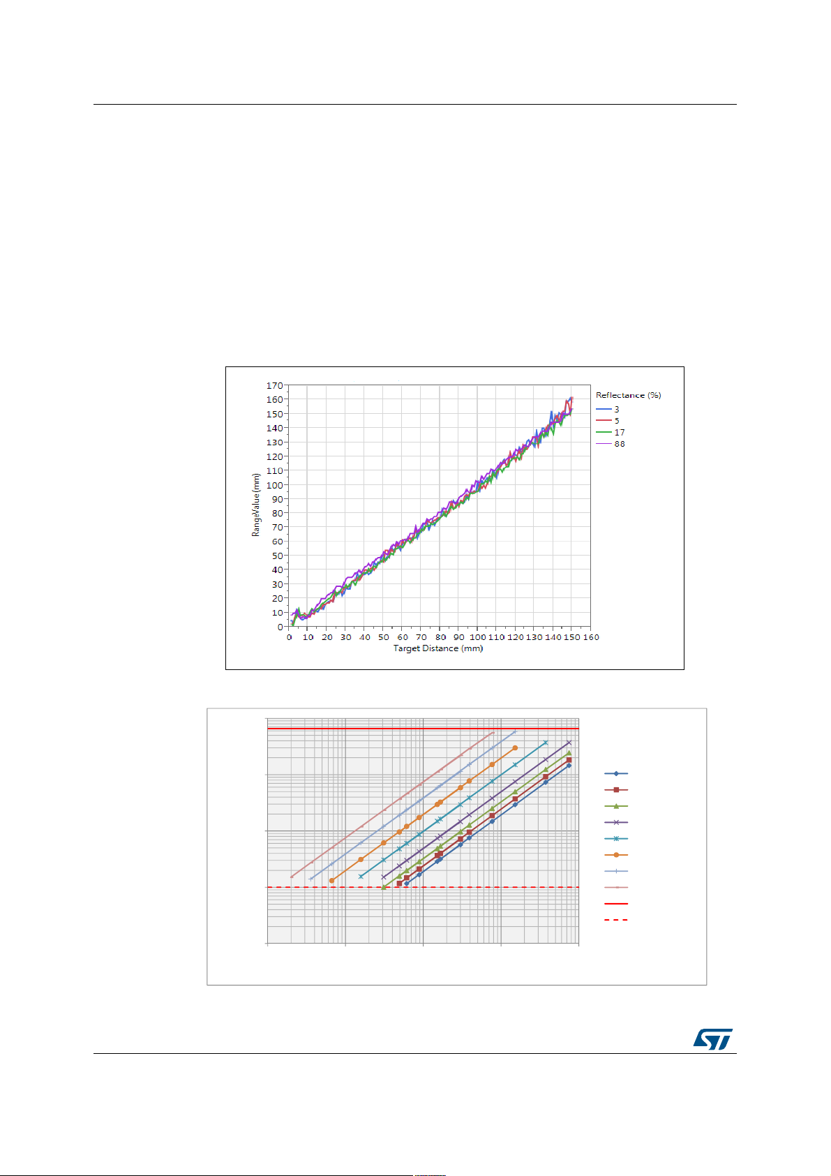
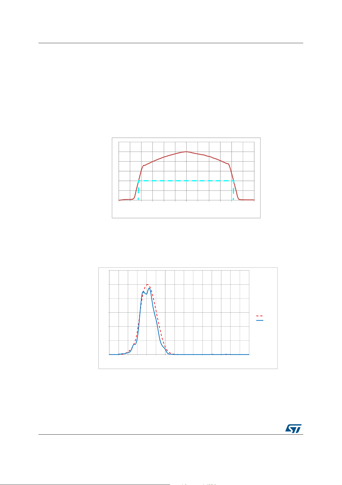
Typical ranging performance of the VL6180X is shown in Figure 6. This demonstrates the
reflectance independence and range accuracy of the VL6180X from 0 to 100 mm for 3%,
5%, 17% and 88% reflective targets. The example shown he re is with ST cover g lass and a
1.0 mm air gap.
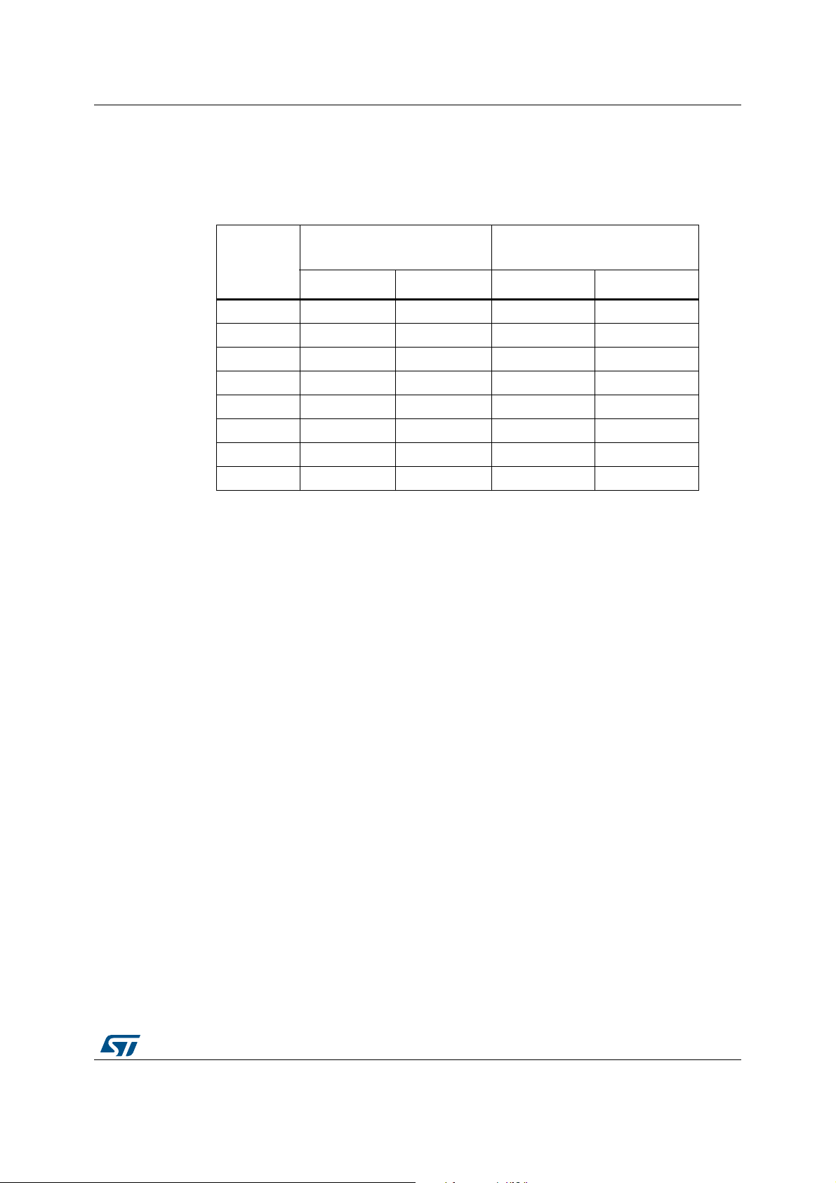
Figure 7 shows typical ALS linearity vs gain over a wide dynamic range. More details about
the ambient light sensor can be found in Section 2.13.
Figure 6. Typical ranging performance
12/79 DocID026171 Rev 6
Figure 7. ALS linearity
Page 13
VL6180X Functional description
Power off
Hardware
standby
Software
standby
Range
measurement
ALS
measurement
Continuous
modes
(*)
AVDD on
GPIO0=0
AVDD off
AVDD on
GPIO0=1
GPIO0=1
GPIO0=0
AVDD off
als_start
range_start
done
done
mode=
continuous
startstop
auto
auto
MCU boot
(*) Device is placed in a low power state between measurements
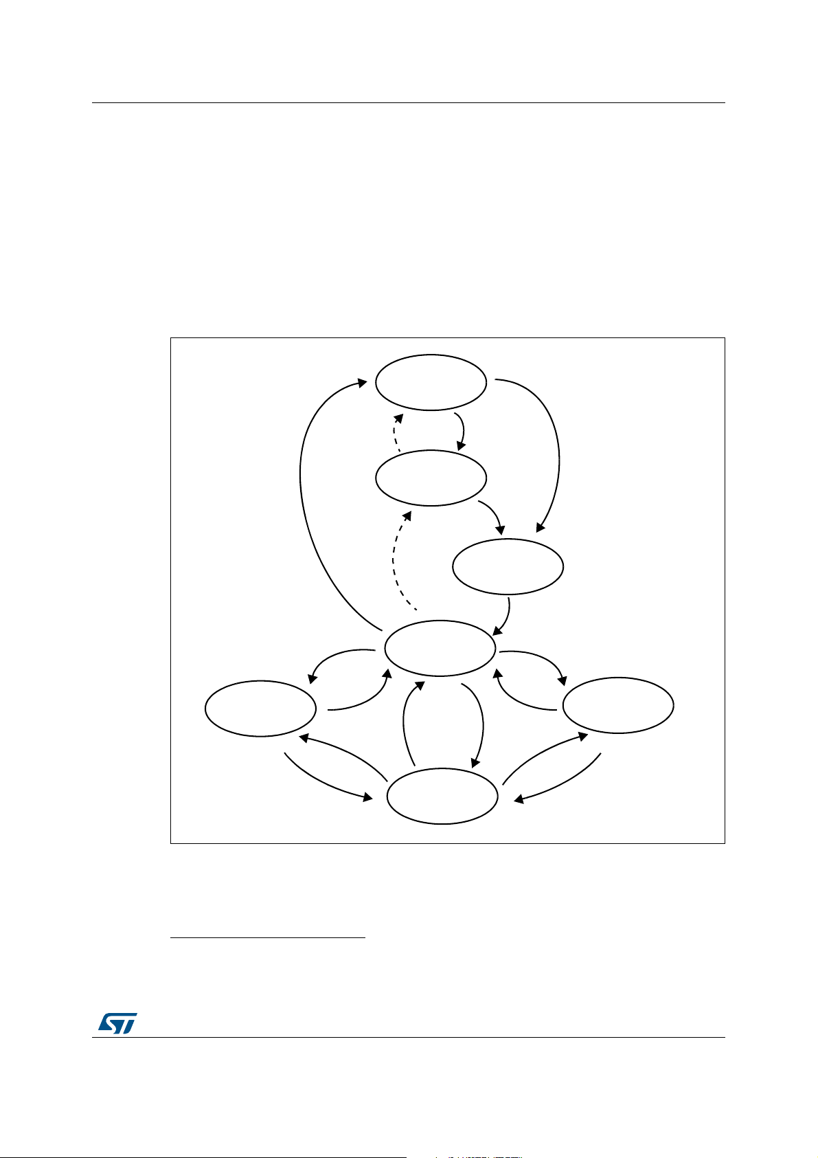
2.1 System state diagram
Figure 8 describes the main operating st ates of the VL6180X. Hardware standby is the reset
state (GPIO0=0)
device will not respond to I
(a)
. The device is held in reset until GPIO0 is de-asserted. Note that the
2
C communication in this mode. When GPIO0=1, the device
enters software standby after the internal MCU boot sequence has completed. Once in
software standby, ST recommended register initialization settings
(b)
can be applied along
with any required application specific register settings. There after, the host can command
single-shot range or ALS measurements or alternatively program one of the continuous
operating modes where the device uses an internal timer to schedule measurement s at
specified intervals. See Section 2.4.3: Interleaved mode.
Figure 8. System state diagram
a. Use of GPIO0 is optional
b. Please contact STMicroelectronics for the latest settings
DocID026171 Rev 6 13/79
78
Page 14
Functional description VL6180X
AVDD
AVDD_VCSEL
GPIO0 (optional)
GPIO1
System state
fresh_out_of_reset
hardware
standby
hardware
standby
software
standby
mcu boot
software
standby
t1
t2
t3
t5
t4
I2C Comms
t3
mcu boot
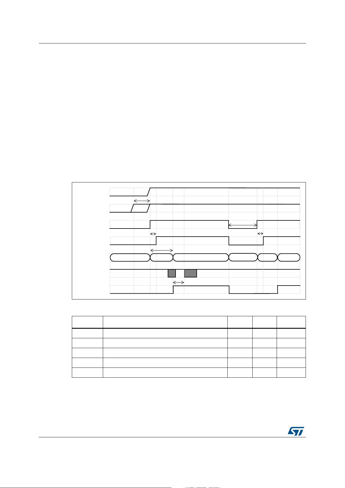
2.2 Timing diagram
Figure 9 and Table 4.show the Root part number 1 power-up timing constraints.
• AVDD_VCSEL must be applied before or at the same time as AVDD.
• GPIO0 defaults to an active low shutdown input. When GPIO0 = 0, the device is in
hardware standby. If GPIO0 is not used it should be connected to AVDD.
• The internal microprocessor (MCU) boot sequence commences when AVDD is up and
GPIO0 is high whichever is the later.
• GPIO1 power-up default is output low. It is tri-stated during the MCU boot sequence.
Note: In hardware standby, GPIO1 is output low and will sink current through any pull-up resistor.
This leakage can be minimized by increasing the value of the pull-up resistor.
• After the MCU boot sequence the device enters software standby. The software
standby state can be determined by polling
SYSTEM__FRESH_OUT_OF_RESET{0x16}. Host initialization can commence
immediately after entering software standby.
Figure 9. Power-up timing
Table 4. Power-up timing constraints
Symbol Parameter Min Max Unit
t1 AVDD_VCSEL power applied after AVDD - 0 ms
t2 Minimum reset on GPIO0 100 - ns
t3 GPIO1 output low after hardware standby - 400 μs
t4 MCU boot - 1 ms
t5 Software standby to host initialization - 0 ms
14/79 DocID026171 Rev 6
Page 15
VL6180X Functional description
Fresh out of
reset?
Software standby
Load initialization
settings
Load application
settings
ALS or range start
Interrupt
status?
Read result and
status
If polling
Power-up
Clear interrupts
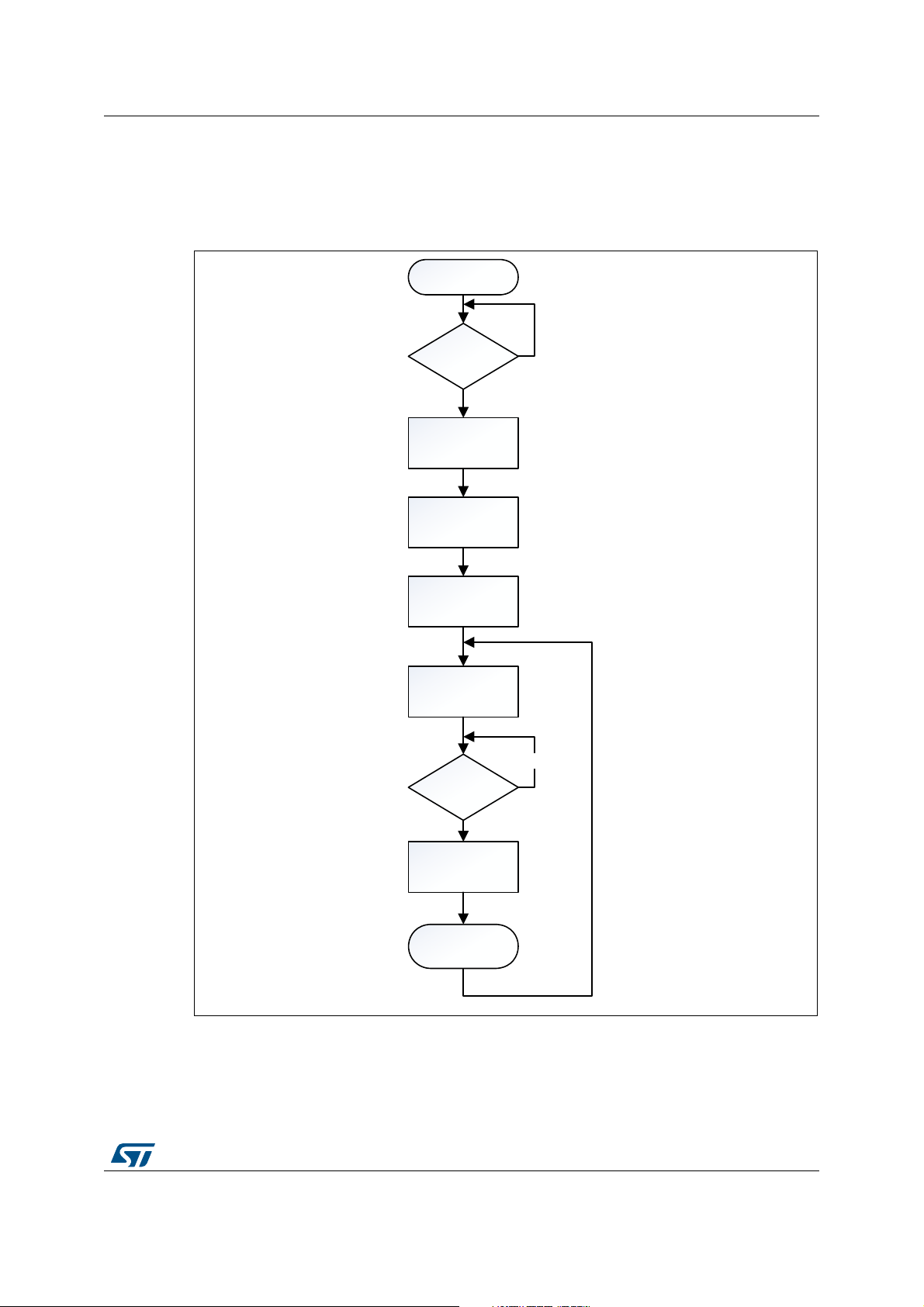
2.3 Software overview
Figure 10 shows a simple start-up routine from initialization to completing a range or ALS
measurement.
Figure 10. Software overview
DocID026171 Rev 6 15/79
78
Page 16
Functional description VL6180X
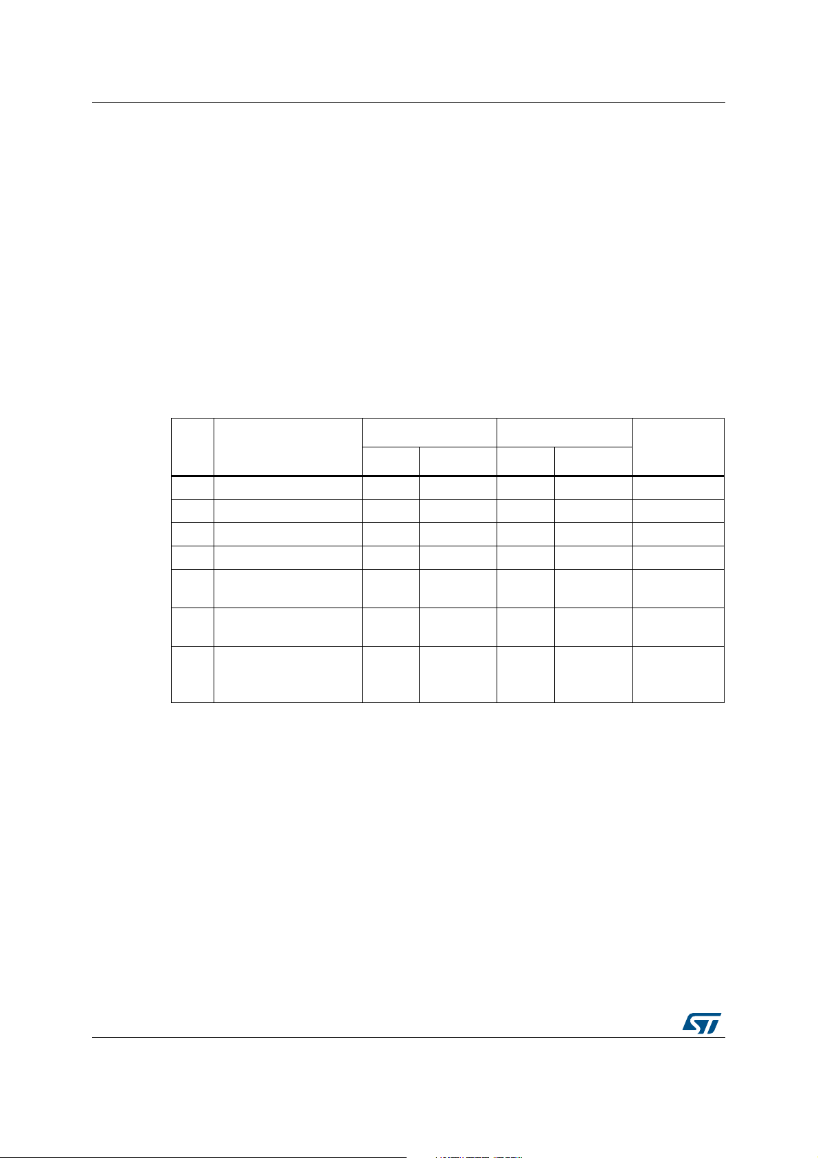
2.4 Operating modes
Table 5. describes the operating modes of this device.
• Modes 1 and 2 are single-shot range and ALS measurements.
• Modes 3 and 4 are stand-alone, continuous operation for either range or ALS.
• Modes 5 and 6 are for mixed continuous and single-shot mode operations where
regular measurements are required from on e of the sensors and only occasional
measurements are required from the other.
Note: In modes 5 and 6, single-shot operation takes the priority i.e. if a scheduled measurement is
in progress when the host requests a single-shot measurement, the scheduled
measurement will be aborted and will resume on the next available time slot.
• Mode 7 al lows both ALS and range measurement s to be scheduled at regu lar intervals.
The ALS measurement is completed first immediately followed by a range
measurement. Interleaved mode is described in more detail in Section 2.4.3.
Table 5. Operating modes
Range ALS
Mode Function
Single Continuous Single Continuous
1 Range single-shot • Range
2 ALS single-shot • ALS
3 Range continuous • Range
Priority
4 ALS continuous • ALS
Range continuous and
5
ALS single-shot
Range single-shot and
6
ALS continuous
Interleaved mode:
7
Range Continuous and
ALS Continuous
••Range
•• ALS
•
•
-
16/79 DocID026171 Rev 6
Page 17

VL6180X Functional description
2.4.1 Single-shot range/ALS operation
A single-shot range or ALS measurement is performed as follows:
• Write 0x01 to the SYSRANGE__START register{0x18}.
• When the measurement is completed, bit 2 of
RESULT__INTERRUPT_STATUS_GPIO{0x4F} will be set.
• Similarly, a single-shot ALS measurement is initiated by writing 0x01 to the
SYSALS__START register{0x38}.
• When the measurement is completed, bit 5 of
RESULT__INTERRUPT_STATUS_GPIO{0x4F} will be set.
Note that in both cases the start bit, (bit 0) auto-clears.
• The range result is read from RESULT__RANGE_VAL{0x62}.
• The ALS result is read from RESULT__ALS_VAL{0x50}.
• Interrupt status flags are cleared by writing a ‘1’ to the appropriate bit of
SYSTEM__INTERRUPT_CLEAR{0x15}.
• Bit 0 of RESULT__RANGE_STATUS{0x4D} and RESULT__ALS_STATUS{0x4E}
indicate when either sensor is ready for the next operatio n.
• Error codes are indicated in bits [7:4] of the status registers
A detailed description of all the user accessible registers is given in Section 6: Device
registers.
Note: Single-shot ALS and range operations cannot be performed simultaneously. Only one of
these operations should be performed at any one time and once started must be allowed to
complete before another measurement is started. This is because any current operation will
be aborted if another is started.
2.4.2 Continuous range/ALS operation
A continuous range or ALS measurement is performed as follows:
• Write 0x03 to the SYSRANGE__START or SYSALS__START registers.
In both cases, bit 1 of the register sets the mode to continuous
• When a measurement is completed either bit 2 or bit 5 of
RESULT__INTERRUPT_STATUS_GPIO{0x4F} will be set.
• Results are read from RESULT__RANGE_VAL{0x62} or
RESULT__ALS_VAL{0x50}.
• Interrupt status flags are cleared by writing a ‘1’ to the appropriate bit of
SYSTEM__INTERRUPT_CLEAR{0x15}.
• Thereafter, measurements will be scheduled according to the relevant inter-
measurement period (see SYSRANGE__INTERMEASUREMENT_PERIOD{0x1B} or
SYSALS__INTERMEASUREMENT_PERIOD{0X3E}).
• Continuous mode operation can be stopped by writing 0 to either START register.
Continuous operation will be halted immediately and any pending measurement will be
aborted.
Note: It is not recommended to run range and ALS continuous modes simultaneously (i.e.
asynchronously). Instead, mode 7 ‘interleaved mode’ in
‘interleaved mode’, scheduled range and ALS measurem ents op erate off a single timer with
a range measurement proceeding immediately after every ALS measurement.
Table 5. should be used. In
DocID026171 Rev 6 17/79
78
Page 18
Functional description VL6180X
ALS
Range
ALS inter-measurement period
ALS inter-measurement period
ALS
Range
ALS
Range
Interrupt
flags
2.4.3 Interleaved mode
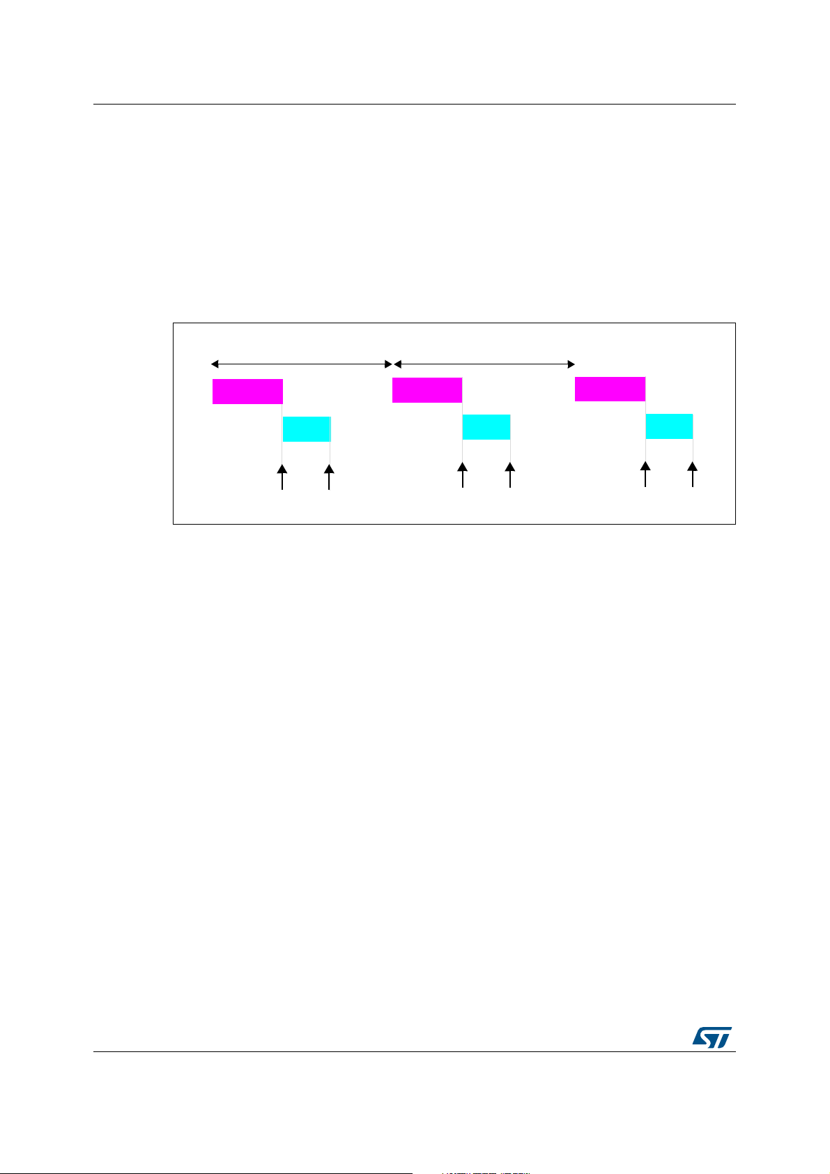
Figure 11. describes the continuous inter lea ve d mo d e of op e ra tio n whe r e an ALS
measurement is immediately followed by a range measurement and repeated after an
interval specified by the ALS inter-measurement period.
To enable interleaved mode, set INTERLEAVED_MODE_ENABLE{0x2A3} = 1. Use
SYSALS__START and SYSALS__INTERMEASUREMENT_PERIOD to control interleaved
operation.
Note: Continuous range settings have no effect in this mode.
Figure 11. Interleaved mode
Note: To ensure correct operation in any of the continuous modes, the user must ensure that the
inter-measurement period is sufficient for the operation to be completed within the intermeasurement period. Failure to do so could result in unpredictable behavior.
2.4.4 Continuous mode limits
To take account of oscillator tolerances and internal processing overheads it is necessary to
place the following constraints on continuous mode operations. The following equations
define the minimum inter-measurement period to ensure correct operation:
Continuous range:
SYSRANGE__MAX_CONVERGENCE_TIME + 5 ≤
SYSRANGE__INTERMEASUREMENT_PERIOD * 0.9
Continuous ALS:
SYSALS__INTEGRATION_TIME * 1.1 ≤ SYSALS__INTERMEASUREMENT_PERIOD *
0.9
Interleaved mode:
(SYSRANGE__MAX_CONVERGENCE _TIME + 5) + (SYSALS__INTEGRATION_TIME *
1.1) ≤ SYSALS__INTERMEASUREMENT_PERIOD * 0.9
Table 6. gives an example how to apply these limits in continuous interleaved mode
operating at a sampling rate of 10 Hz.
18/79 DocID026171 Rev 6
Page 19
VL6180X Functional description
Readout
averaging
Range convergencePre-cal
4.3 ms
Convergence time
(variable)
Table 6. Interleaved mode limits (10 Hz operation)
Parameter Period (ms)
SYSALS__INTERMEASUREMENT_PERIOD
Effective ALS INTERMEASUREMENT PERIOD
SYSRANGE__MAX_CONVERGENCE_TIME
Total RANGE EXECUTION TIME
SYSALS__INTEGRATION_TIME
Total ALS INTEGRATION TIME
TOTAL EXECUTION TIME
100
90
30
35
50
55
90
2.5 Range timing
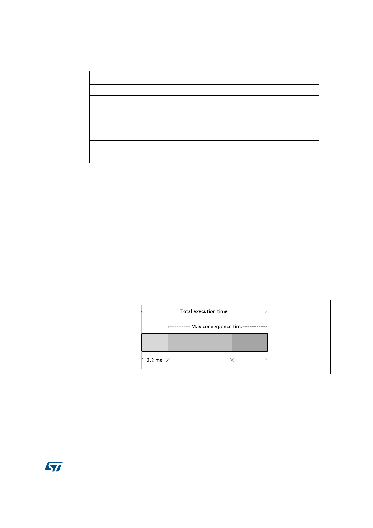
Figure 12 gives a breakdown of total execution time for a single range measurement.
• The pre-calibration phase is fixed (3.2 ms).
• The range co nvergence time is variable and depends on target distance/r efle ctance
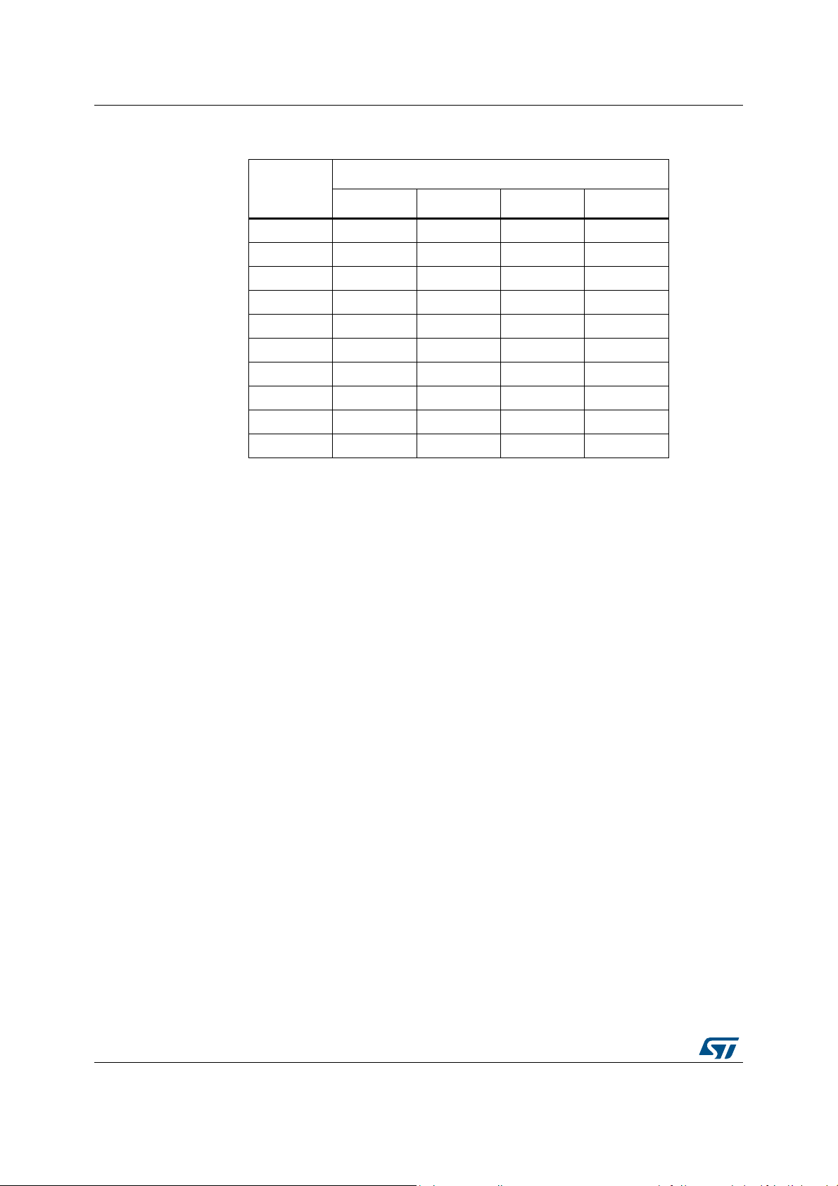
(see Table 7).
• The recommended readout averaging period is 4.3 ms. Readout averaging helps to
reduce measurement noise. The recommended setting for
READOUT__AVERAGING_SAMPLE_PERIOD{0x10A} is 48
the range 0-255. Note however that lower settings will result in increased noise.
Note: When a target is detected, register RESULT__RANGE_RETURN_CONV_TIME{0x80} returns
the actual convergence time before readout averaging. Range convergence and readout
averaging must be completed within the specified max convergence time.
(c)
but is programmable in
Figure 12. Total range execution time
c. Default readout averaging period is calculated as follows: 1300 µs + (48 x 64.5 µs) = 4.3 ms
DocID026171 Rev 6 19/79
78
Page 20
Functional description VL6180X
Table 7. Typical range convergence time (ms)
Ta rget reflectance
Range (mm)
3% 5% 17% 88%
10 0.43 0.33 0.18 0.18
20 0.94 0.73 0.28 0.18
30 1.89 1.40 0.51 0.18
40 3.07 2.25 0.81 0.18
50 4.35 3.24 1.18 0.24
60 5.70 4.22 1.60 0.32
70 7.07 5.35 2.07 0.49
80 8.41 6.45 2.58 0.50
90 9.58 7.56 3.14 0.61
100 10.73 8.65 3.69 0.73
2.6 Interrupt modes
The VL6180X can be configured to generate an ALS or range inte rrupt flag under any of the
following conditions:
• New sample ready
• Level low (RESULT__RANGE_VAL < SYSRANGE__THRESH_LOW)
• Level high (RESULT__RANGE_VAL > SYSRANGE__THRESH_HIGH)
• Out of window (RESULT__RANGE_VAL < SYSRANGE__THRESH_LOW) OR
(RESULT__RANGE_VAL > SYSRANGE__THRESH_HIGH)
In new sample ready mode, an interrupt flag will be raised at the end of every measurement
irrespective of whether the measurement is valid or if an error has occurred. This mode is
particularly useful during development and debug. In level interrupt mode the system will
raise an interrupt flag if either a low or high programmable threshold has been crossed. Out
of window interrupt mode activates both high and low level thresholds allowing a window of
operation to be specified. Interrupt modes for Range and ALS are configured via register
SYSTEM__INTERRUPT_CONFIG_GPIO{0x14}.
Note: In level or window interrupt modes range errors will only trigger an interrupt if the logical
conditions described above are met.
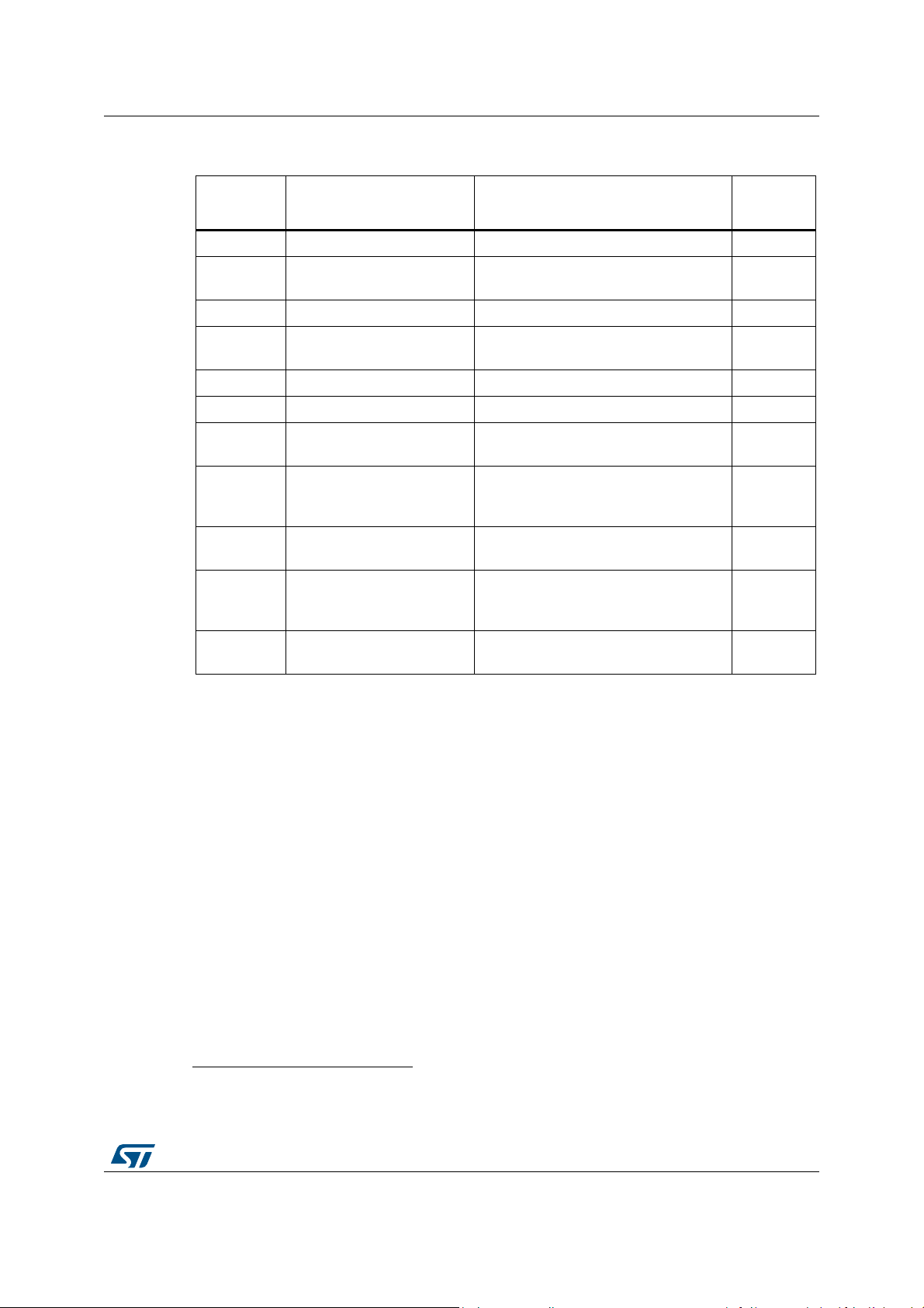
2.7 Range error codes
The system carries out a number of range checks during every range measurement to
ensure the validity of each range result. Register RESULT__RANGE_STATUS{0x4D}
returns an error code if one of the checks fails. Table 8 gives a summary of the possible
error codes.
20/79 DocID026171 Rev 6
Page 21
VL6180X Functional description
Table 8. Range error codes
Bits [7:4] Error code Description
0 No error Valid measurement 0 - 200
1-5 System error
6 Early convergence estimate ECE check failed 255
7 Max convergence
8 Range ignore Ignore threshold check failed 255
9-10 Not used - -
11 SNR
12 Raw range underflow
13 Raw range overflow
14 Range underflow
System error detected. No
measurement possible.
System did not converge before the
specified max. convergence time limit
Ambient conditions too high.
Measurement invalidated
RESULT__RANGE_RAW < 0
(because offset is programmable a
negative range result is possible)
RESULT__RANGE_RAW is out of range.
This occurs typically around 200 mm
RESULT__RANGE_VAL < 0
(because offset is programmable a
negative range result is possible)
Range
(mm)
(1)
255
255
255
0
255
0
15 Range overflow
1. Range overflow occurs typically around 200 mm.
RESULT__RANGE_VAL is out of range.
This occurs typically around 200 mm
2.8 Range checks
Error codes 6, 8 and 11 in Table 8 are configurable by the user. They can be
enabled/disabled via register SYSRANGE__RANGE_CHECK_ENABLES{0x2D} by setting or
clearing the appropriate bit. The register default is 0x11 i,e, ECE and SNR enabled.
2.8.1 Early convergence estimate (ECE)
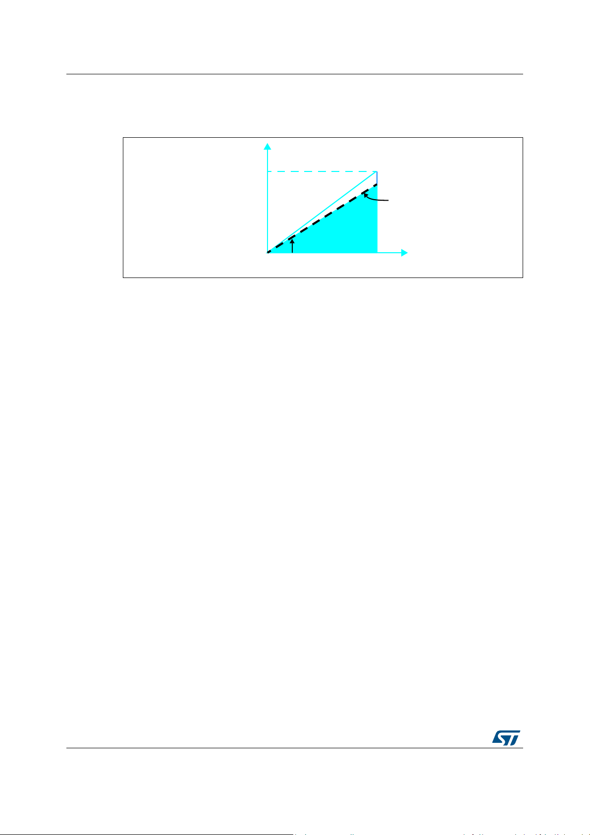
Early convergence estimate (ECE) is a progra m m abl e fe at ur e de sig ne d to mi nim iz e po we r
consumption when there is no target in the field-of-view (FOV).
The system is said to have ‘converged’ (i.e. range acquired), when the convergence
threshold
specifies the minimum return signal rate required for convergence. If there is no target in the
FOV, the system will continue to operate until the max. convergence time limit is reached
before switching off thereby consuming power. With ECE enabled, the system estimates the
d. For standard ranging, the convergence threshold is set to 15360. The convergence threshold register is not
(d)
is reached before the max. convergence time limit (see Figure 13). This ratio
accessible by the user.
255
DocID026171 Rev 6 21/79
78
Page 22
Functional description VL6180X
time
Return
count
convergence threshold
m
i
n
.
r
e
t
u
r
n
s
i
g
n
a
l
r
a
t
e
max.
convergence
ECE (0.5 ms)
measurement
aborted
converged
ECE
threshold
ECE threshold
80% 0,5× 15360×
SYSRANGE__MAX_CONVERGENCE_TIME (in ms)
----------------------------------------------------------------------------------------------------------------------------------------=
SYSRANGE__RANGE_IGNORE_THRESHOLD{0x26} cross-talk (Mcps) 120%×=
return signal rate 0.5 ms after the start of every measurement. If it is below the ECE
threshold, the measurement is aborted and an ECE error is flagged.
Figure 13. Early convergence estimate (ECE)
ECE is enabled by setting bit 0 of SYSRANGE__RANGE_CHECK_ENABLES{0x02D}. If
enabled, the ECE threshold must be specified. To set the ECE threshold 20% below the
minimum convergence rate, the ECE threshold is calculated as follows:
The 16-bit ECE threshold should be written to
SYSRANGE__EARLY_CONVERGENCE_ESTIMATE{0x22}. For example, if
SYSRANGE__MAX_CONVERGENCE_TIME{0x1c} is set to 30 ms, the ECE threshold is 204.
If the return count is less than 204 after 0.5 ms, the measurement will be aborted.
Note: The optimum value for the ECE threshold should be determined in the final application.
2.8.2 Range ignore
In a system with cover glass, the return signal from the glass (cross-talk) may be sufficient
to cause the system to converge and return a valid rang e m easu rement e ven wh en ther e is
no target present. The range ignore feature is designed to ensure that the system does not
range on the glass. (Cross-talk is described in more detail in Section 2.12.2).
The ignore threshold is enabled by setting bit 1 of
SYSRANGE__RANGE_CHECK_ENABLES{0x02D}. If enabled, the ignore threshold must be
specified. In the follow example, the ignore threshold is set 20% above the system crosstalk:
A range ignore error will be flagged if the return signal rate is less than the ignore threshold.
SYSRANGE__RANGE_IGNORE_VALID_HEIGHT should be set to 255.
Note: The optimum value for the ignore threshold should be determined in the final application.
22/79 DocID026171 Rev 6
Page 23

VL6180X Functional description
SNR
RESULT__RANGE_RETURN_SIGNAL_COUNT{0x6C}
RESULT__RANGE_RETURN_AMB_COUNT{0x74} * 6
---------------------------------------------------------------------------------=
2.8.3 Signal-to-noise ratio (SNR)
In high ambient conditions range accuracy can be impaired so the SNR threshold is used as
a safety limit to invalidate range measurements where the ambient/signal ratio is considered
too high.The default ambient/signal ratio limit is 10 (i.e. an SNR of 0.1) which is then
encoded in 4.4 format as follows:
SYSRANGE__MAX_AMBIENT_LEVEL_MULT{0x2C}= 10 x 16 = 160
To enable the SNR check, set bit 4 in SYSRANGE__RANGE_CHECK_ENABLES (0x02D). A
lower setting results in a more aggressive filter which will result in a lower effective range but
greater accuracy. A higher setting results in a less aggressive filter which will result in a
greater effective range but lower accuracy.
The SNR value can be calculated as follows:
Note: The SNR value is the inverse of the ambient/signal ratio limit {0x2C}.
Note: The optimum value for SNR threshold should be determined in the final application.
2.9 Manual/autoVHV calibration
(e)
SPAD
sensitivity is temperature dependent so VHV
sensitivity over temperature in order to minimize signal rate variation. VHV calibration is
performed either manually by the host processor or automatically by internal firmware.
Execution time is typically 200 μs so has no impact on normal operation.
A VHV calibration is run once at power-up and then automatically after every N range
measurements defined by the SYSRANGE__VHV_REPEAT_RATE{0x31} register.
AutoVHV calibration is disabled by setting this register to 0. Default is 255. If autoVHV is
disabled it is recommended to run a manual VHV calibration periodically to recalibrate for
any significant temperature variation. A manual VHV calibration is performed by setting
SYSRANGE__VHV_RECALBRATE{0x2E} to 1. This register auto-clears. This operation
should only be performed in software standby.
2.10 History buffer
The history buffer is a 8 x 16-bit memory which can be used to store the last 16 range
measurements (8-bit) or 8 ALS samples (16-bit). Use of the history buffer is controlled via
register SYSTEM__HISTORY_CTRL{0x12}. There are 3 basic functions:
• enable
• range or ALS selection
• clear buffer
(f)
calibration is used to regulate SPAD
e. Photon detectors - Single Photon Avalanche Diodes
f. VHV is an adjustable SPAD bias voltage and stands for Very High Voltage (typically around 14 V). Also
sometimes referred to as CP (Charge Pump).
DocID026171 Rev 6 23/79
78
Page 24
Functional description VL6180X
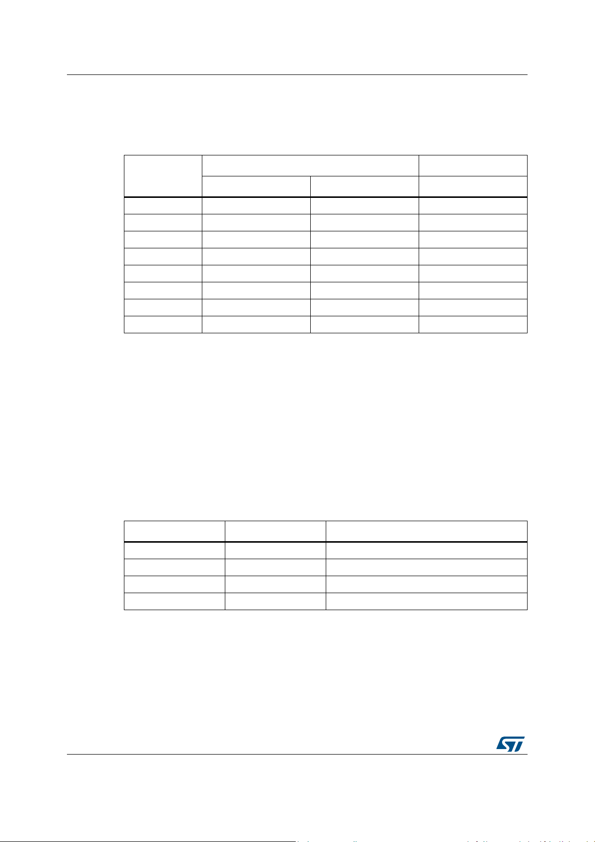
The buffer is read via eight 16-bit registers (RESULT__HISTORY_BUFFER_0{0x52} to
RESULT__HISTORY_BUFFER_7{0x60}). The buffer holds the last 16 x 8-bit range or 8 x
16-bit ALS results as shown in Table 9.
Table 9. History buffer
Range ALS
History buffer
(High byte) (Low byte) (Word)
0 Range [15] (newest) Range [14] ALS [7] (newest)
1 Range [13] Range [12] ALS [6]
2 Range [11] Range [10] ALS [5]
3 Range [9] Range [8] ALS [4]
4 Range [7] Range [6] ALS [3]
5 Range [5] Range [4] ALS [2]
6 Range [3] Range [2 ALS [1]
7 Range [1] Range [0] (oldest) ALS [0] (old est)
Note: Only one data stream (ALS or range) can be buffered at one time. There is no associated
time stamp information.
The clear buffer command is not immediate; it takes effect on the next range or ALS start
command.
The history buffer works independently of interrupt control i.e. the history buffer records all
new samples; its operation is unchanged in threshold and window modes.
2.11 Current consumption
Table 10. gives an overview of current consumption in different operating states.
Table 10. Typical current consumption in different operating states
Mode Current Conditions
2
Hardware standby < 1 μA Shutdown (GPIO0 = 0). No I
Software standby < 1 μA After MCU boot. Device ready
ALS 300 μA During integration
Ranging 1.7 mA Average consumption during rangi ng
1. 10 Hz sampling rate, 17% reflective target at 50 mm.
C comms
(1)
2.11.1 Ranging current consumption
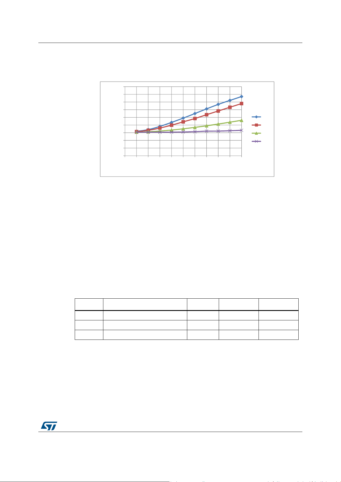
Figure 14. shows typical ranging current consumption of the VL6180X. Current consumption
depends on target distance, t arget r eflect ance and sampling rate. The example shown here
is based on default settings and a sampling rate of 10 Hz. The average current consumption
for a 17% reflective target at 50 mm operating at 10 Hz is 1.7 mA. At dif ferent sampling rates
24/79 DocID026171 Rev 6
Page 25
VL6180X Functional description
ϬϬϬ
ϬϱϬ
ϭϬϬ
ϭϱϬ
ϮϬϬ
ϮϱϬ
ϯϬϬ
ϯϱϬ
ϰϬϬ
ϰϱϬ
Ϭ ϭϬϮϬϯϬϰϬϱϬϲϬϳϬϴϬϵϬϭϬϬ
ƵƌƌĞŶƚĐŽŶƐƵŵƉƚŝŽŶ;ŵͿ
ZĂŶŐĞ;ŵŵͿ
ϯй
ϱй
ϭϳй
ϴϴй
the current consumption scales accordingly i.e. the average current consumption at 1 Hz
under the same conditions would be 0.17 mA.
Figure 14. Typical ranging current consumption (10 Hz sampling rate)
The minimum average current consumption in Figure 14. is 1.5 mA, 0.5 mA of which com es
from pre-calibration before each measurement and 1.0 mA from post-processing (readout
averaging). Pre-calibration is a fixed overhead but readout averaging can be reduced or
effectively disabled by setting the READOUT__AVERAGING_SAMPLE_PERIOD{0x10A} to
zero (default setting is 48).
Note: Decreasing the READOUT__AVERAGING_SAMPLE_PERIOD will increase sampling
noise. It is recommended that any change in setting be properly
evaluated in the end application.
Minimum current consumption scales with sampling rate i.e. at a sampling rate of 1 Hz the
current consumption associated with pre- and post-processing will be 0.15 μA.
2.11.2 Current consumption calculator
Table 11. gives a breakdown of typical current consumption for pre-calibration, ranging and
readout averaging.
Label Phase I (mA) t (ms) Q (μC) = I x t
Q
Q
Q
Current consumption can then be calculated as follows:
I (
μA) = sampling_rate * [Q
Q
* (1.3 + (READOUT__AVERAGING_SAMPLE_PERIOD * 0.0645 ms))]
3
Table 7. gives typical convergence times for different target reflect ance.
So, for example, RESULT__RANGE_RETURN_CONV_TIME for a 3% target at 50 mm
is 4.35 ms. At 10 Hz sampling rate this gives:
I (
μA) = 10 * [41.6 + (22 * 4.35) + 25 * (1.3 + (48 * 0.0645))] = 2472 μA
Pre-calibration 13.0 3.2 41.6
1
Ranging 22.0 per ms 22.0 per ms
2
Readout averaging 25.0 per ms 25.0 pe r ms
3
Table 11. Brea kdown of current consumption
+ (Q2 * RESULT__RANGE_RETURN_CONV_TIME in ms) +
1
DocID026171 Rev 6 25/79
78
Page 26
Functional description VL6180X
33% duty cycle
10 ns
24 mA peak current
8 mA average current
2.11.3 Current distribution
T able 12. shows how current consumption is distributed between the two su pplies in ranging
mode. AVDD_VCSEL supplies the VCSEL current and AVDD supplies all other functions.
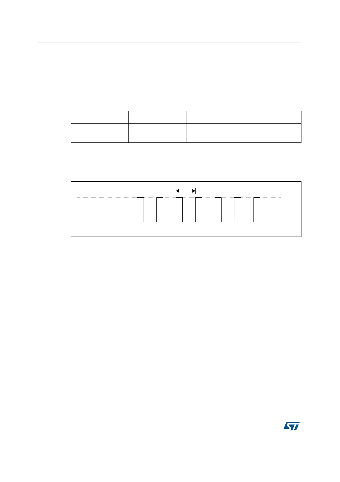
Note: The VCSEL driver is pulsed at 100 MHz with a 33% duty cycle (see Figure 15.) so average
current consumption on AVDD_VCSEL is one third of the peak.
Table 12. Current consumption on AVDD and AVDD_VCSEL
Power supply
AVDD 14 mA Average during active ranging
AVDD_VCSEL 8 mA
1. Normally, both supplies will be driven from a common source giving a peak instantaneous current demand
of 38 mA.
2. Peak emitter current during ranging is 24 mA.
(1)
Current Note
(2)
Average during active ranging (33% duty cycle).
Figure 15. VCSEL pulse duty cycle
26/79 DocID026171 Rev 6
Page 27
VL6180X Functional description
Actual Range
Measured range
p2p_offset
calibration
Actual Range
Measured range
cross-talk
compensation
2.12 Other system considerations
This section describes part-to-part range offset and system cross-talk. In addition, a
procedure for cross-talk calibration is given.
2.12.1 Part-to-part range offset
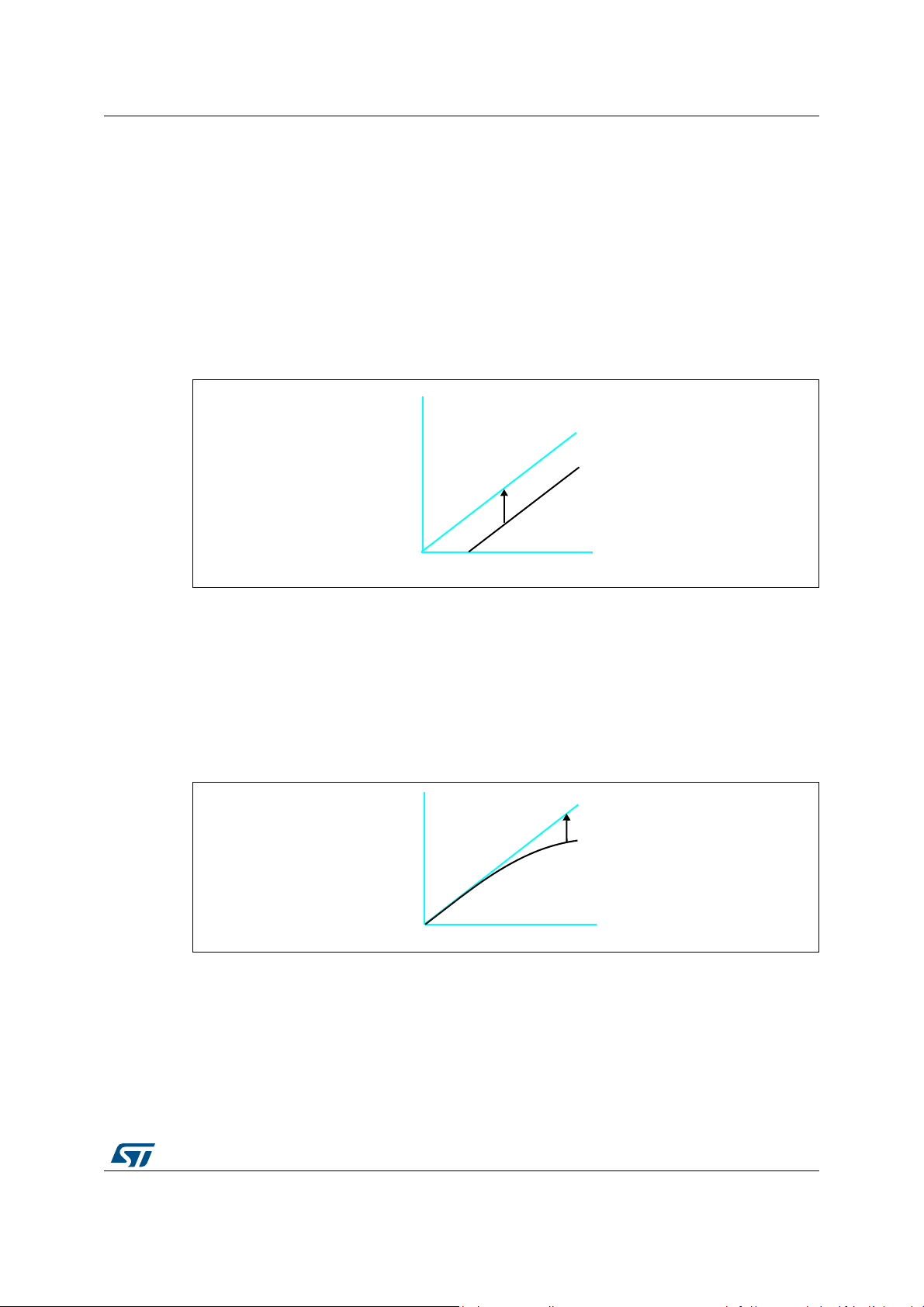
The VL6180X is factory calibrated to produce an absolute linear range output as shown in
Figure 16. The part-to-part range offset is calibrated during manufacture and stored in
SYSRANGE__PART_TO_PART_RANGE_OFFSET{0x24} (two’s complement).
RESULT__RANGE_RAW{0x64} reports the range with the part -to-part of fset already applied.
Figure 16. Part-to-part range offset
2.12.2 Cross-talk
Cross-talk is defined as the signal return from the cover glass. The magnitude of the crosstalk depends on the type of glass, air gap and filter material. Cross-talk results in a range
error (see Figure 17) which is proportional to the ratio of the cross-talk to the signal return
from the target. The true range is recovered by applying automatic cross-talk compensation.
Figure 17. Cross-talk compensation
To enable cross-talk compensation it is necessary to write the calibrated cross-talk value to
SYSRANGE__CROSSTALK_COMPENSATION_RATE{0x1E}in 9.7 format. A cross-talk
calibration procedure is described in Section 2.12.4.
2.12.3 Offset calibration procedure
Complete steps 1-3 to see if part-to-part offset calibration is required.
DocID026171 Rev 6 27/79
78
Page 28

Functional description VL6180X
part-to-part offset 50 mm average range–=
cross-talk (in Mcps) average return rate 1
average range
100 mm
--------------------------------------–
×=
1. Position a white target (88% reflectance
(g)
) at a distance of 50 mm from the top of the
cover glass.
2. Perform a minimum of 10 range measurements and compute the average range (from
RESULT__RANGE_VAL{0x62}).
3. If the average range is within the 50 ± 3 mm, offset calibration is not required.
Otherwise, complete this calibration procedure.
4. Set SYSRANGE__PART_TO_PART_RANGE_OFFSET{0x24} = 0.
5. Perform a minimum of 10 range measurements and compute the average range (from
RESULT__RANGE_VAL{0x62}).
6. Calculate the part-to-part offset as follows:
7. Write the part-to-part offset result (in two’s complement notation) to
SYSRANGE__PART_TO_PART_RANGE_OFFSET.
2.12.4 Cross-talk calibration procedure
This section describes a procedure for calibrating system cross-talk.
1. Perform offset calibration if required (see Section 2.12.3).
Note: If the offset is incorrectly calibrated, cross-talk calibration will be inaccurate.
2. Position a black target (3% reflectance
cover glass.
3. Ensure SYSRANGE__CROSSTALK_COMPENSATION_RATE{0x1E} = 0.
4. Perform a minimum of 10 range measurements and compute the average return rate
(from
RESULT__RANGE_RETURN_RATE{0x66}) and the average range (from
RESULT__RANGE_VAL{0x62}).
5. Ca lcu lat e th e cro ss-talk factor as follows:
(h)
) at a distance of 100 mm from the top of the
6. Write the cross-talk result in 9.7 format to
SYSRANGE__CROSSTALK_COMPENSATION_RATE.
For example, cross-talk = 0.4 Mcps => 0.4 x 128 = 51.2. Write 51 to
SYSRANGE__CROSSTALK_COMPENSATION_RATE.
Note: Cross-talk compensation is only applied to targets above 20 mm. This is to ensure that
cross-talk correction is not applied to near targets where the signal rate is decreasing. The
cross-talk height qualifier is defined in register
SYSRANGE__CROSSTALK_VALID_HEIGHT{0x21}. The default is 20 mm.
g. Target reflectance should be high but absolute value is not critical.
h. Target reflectance should be low but absolute value is not critical.
28/79 DocID026171 Rev 6
Page 29
VL6180X Functional description
Ϭ
ϬϮ
Ϭϰ
Ϭϲ
Ϭϴ
ϭ
ϭϮ
ϭϰ
ϭϲ
ϬϬϱϭϭϱϮϮϱ
ƌŽƐƐƚĂůŬ;DĐƉƐͿ
ŝƌŐĂƉ;ŵŵͿ
2.12.5 Cross-talk limit
A practical limit for cross-talk is < 3.0 Mcps. This is based on two factors:
1. The return rate for a 3% reflective target at 100 mm without glass is typically around 1.5
Mcps. If glass is added with a cross-talk of 3.0 Mcps, the resultant return rate will be 4.5
Mcps. This results in a cross-talk corre ction factor of x3 so for a 100 mm t ar get the raw
range will be in the region of 30 mm. To ensure the
SYSRANGE__CROSSTALK_VALID_HEIGHT restriction is not breached, the minimum
raw range allowing for noise margin is around 30 mm.
2. A cross-talk correction factor of x3 also means that any range noise will be multiplied
by 3 so noise also becomes a limiting factor.
2.12.6 Cross-talk vs air gap
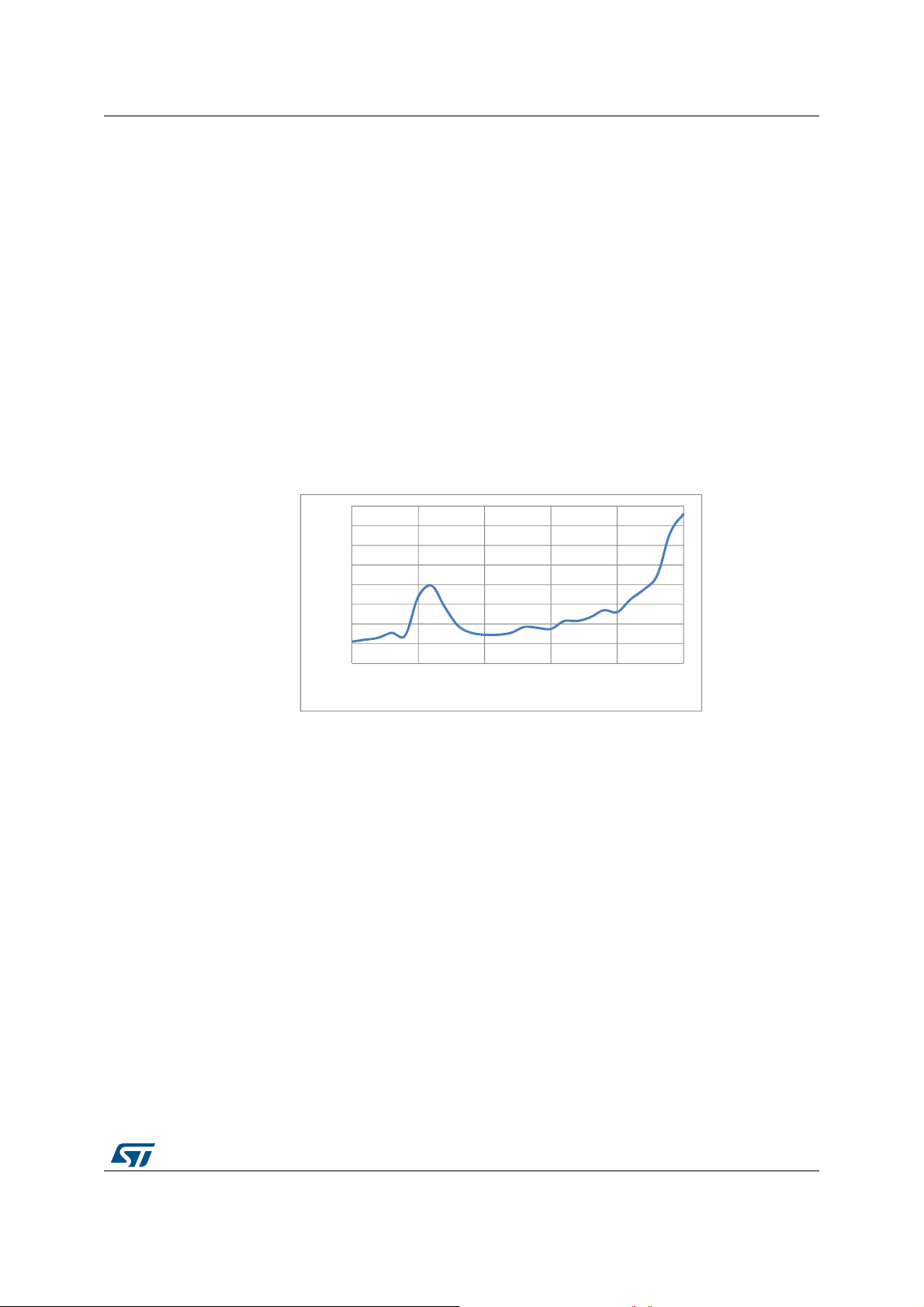
Figure 18 shows the typical cross-talk vs air gap using ST cover glass with oval aperture.
Above 2.5 mm, the cross-talk rises rapidly.
Figure 18. Cross-talk vs air gap
DocID026171 Rev 6 29/79
78
Page 30
Functional description VL6180X
Ϭ
ϬϮ
Ϭϰ
Ϭϲ
Ϭϴ
ϭ
ϭϮ
ͲϲϬͲϱϬͲϰϬͲϯϬͲϮϬͲϭϬ Ϭ ϭϬϮϬϯϬϰϬϱϬϲϬ
ŶŐůĞ;ΣͿ
0%
20%
40%
60%
80%
100%
120%
350 400 450 500 550 600 650 700 750 800 850 900 950 1000 1050 1100
Wavelength (nm)
Photopic
VL6180X
2.13 Ambient light sensor (ALS)
The VL6180X contains an ambient light sensor cap able of measuring the ambient light level
over a wide dynamic range. This section describes the main features of the ALS. The ALS
performance specification can be found in Section 4.2.
2.13.1 Field of view
Figure 19 shows the ALS field of view which is typically 42 degrees (half angle, 40% of
peak) in both X and Y.
Figure 19. ALS angular response
2.13.2 Spectral response
The spectral response of the ALS compared to photopic response is shown in Figure 20.
Figure 20. ALS spectral response
30/79 DocID026171 Rev 6
Page 31
VL6180X Functional description
Light level (in lux) ALS lux resolution
RESULT__ALS_VAL
Analog gain
------------------------------------------------------- -
100 ms
ALS integration time
----------------------------------------------------- -××=
ALS lux resolution (with glass)
RESULT__ALS_VAL (without glass)
RESULT__ALS_VAL (with glass)
--------------------------- -------------------------------------------------------- ------------- ALS lux resolution (without glass)×=
2.13.3 ALS dynamic range
Table 13 shows the range of measurable light at all gains both with and without glass. In
most applications operating at a single gain setting should be possible.
Table 13. ALS dynamic range
(1)
Analogue
gain setting
Dynamic range (no glass)
Min. (Lux)
(2)
1 3.20 20800 32.0 >100,000
1.25 2.56 16640 25.6 >100,000
1.67 1.93 12530 19.3 >100,000
2.5 1.28 8320 12.8 83,200
5 0.64 4160 6.4 41,600
10 0.32 2080 3.2 20,800
20 0.16 1040 1.6 10,400
40 0.08 520 0.8 5,200
1. ALS lux resolution = 0.32 lux/count
2. Minimum of 10 counts
2.13.4 ALS count to lux conversion
The output from the ambient light sensor is a 16-bit register, RESULT__ALS_VAL{0x50}.
The count output is proportional to the light level and can be converted into lux using the
following equation:
Dynamic range (10%
transmissive glass)
Max. (Lux) Minimum (Lux) Maximum (Lux)
The factory calibrated ALS lux resolution is 0.32 lux/count for an analog gain of 1 (calibrated
without glass). The ALS lux resolution will require re-calibration in the final system where
cover glass is used. This can be done by recording the count output with and without glass
under the same conditions and multiplying the ALS lux resolution by the ratio of the two
counts as follows:
DocID026171 Rev 6 31/79
78
Page 32
Functional description VL6180X
2.13.5 Integration period
The integration period is the time over which a single ALS measurement is made. The
default integration period is 100ms. Integration times in the range 50-100 ms are
recommended to reduce impact of light flicker from artificial lighting.
2.13.6 ALS gain selection
Eight analog gain settings are available which can be selected manually depending on the
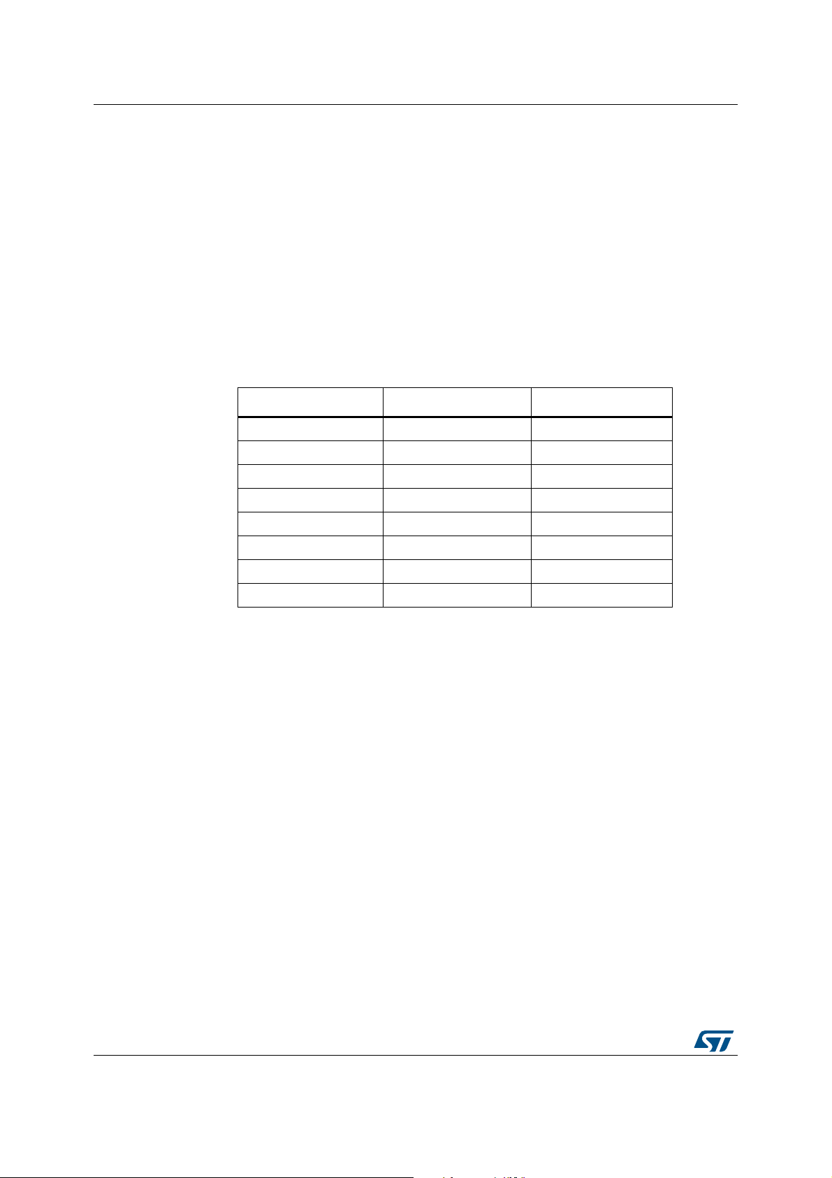
range and resolution required. Table 14.shows the actual characterized gains versus the
design targets. If a gain setting other than gain 20 is used, marginally greater accuracy can
be achieved by using the actual gain values in the light level equation in Section 2.13.4
when calculating the lux light level.
Table 14. Actual gain values
Register setting {0x3F} Analog gain setting Actual gain values
0x46 1 1.01
0x45 1.25 1.28
0x44 1.67 1.72
0x43 2.5 2.60
0x42 5 5.21
0x41 10 10.32
0x40 20 20
0x47 40 40
Note: The upper nibble of SYSALS__ANALOGUE_GAIN should always be set to 0x4.
32/79 DocID026171 Rev 6
Page 33
VL6180X Electrical characteristics
3 Electrical characteristics
3.1 Absolute maximum ratings
Table 15. Absolute maximum ratings
Parameter Min. Typ. Max. Unit
AVDD -0.5 - 3.6 V
AVDD_VCSEL -0.5 - 3.6 V
SCL, SDA, GPIO0 and GPIO1 -0.5 - 3.6 V
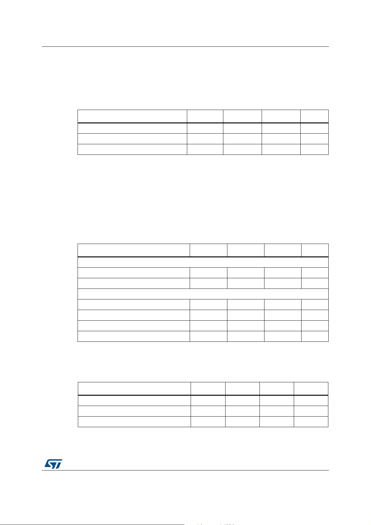
Note: Stresses above those listed in Table 15. may cause permanent damage to the device. This
is a stress rating only and functional operation of the device at these or any other conditions
above those indicated in the operational sections of the specification is not implied.
Exposure to absolute maximum rating conditions for extended periods may affect device
reliability.
3.2 Normal operating conditions
Parameter Min. Typ. Max. Unit
Voltage (AVDD and AVDD_VCSEL)
Voltage (optimum operating) 2.7 2.8 2.9 V
Voltage (functional operating) 2.6 2.8 3.0 V
Temperature
Temperature (optimum operating) -10 +60 °C
Temperature (functional operating) -20 - +70 °C
Temperature (test) +21 - +25 °C
Temperature (storage) -40 - +85 °C
Table 16. Normal operating conditions
3.3 Current consumption
Parameter Min. Typ. Max. Unit
Hardware Standby - - 1 µA
Software Standby - - 1 µA
ALS operation - 300 350 µA
Table 17. Current consumption
(1)
1. Measured at room temperature (23°C)
DocID026171 Rev 6 33/79
78
Page 34
Electrical characteristics VL6180X
3.4 Electrical characteristics
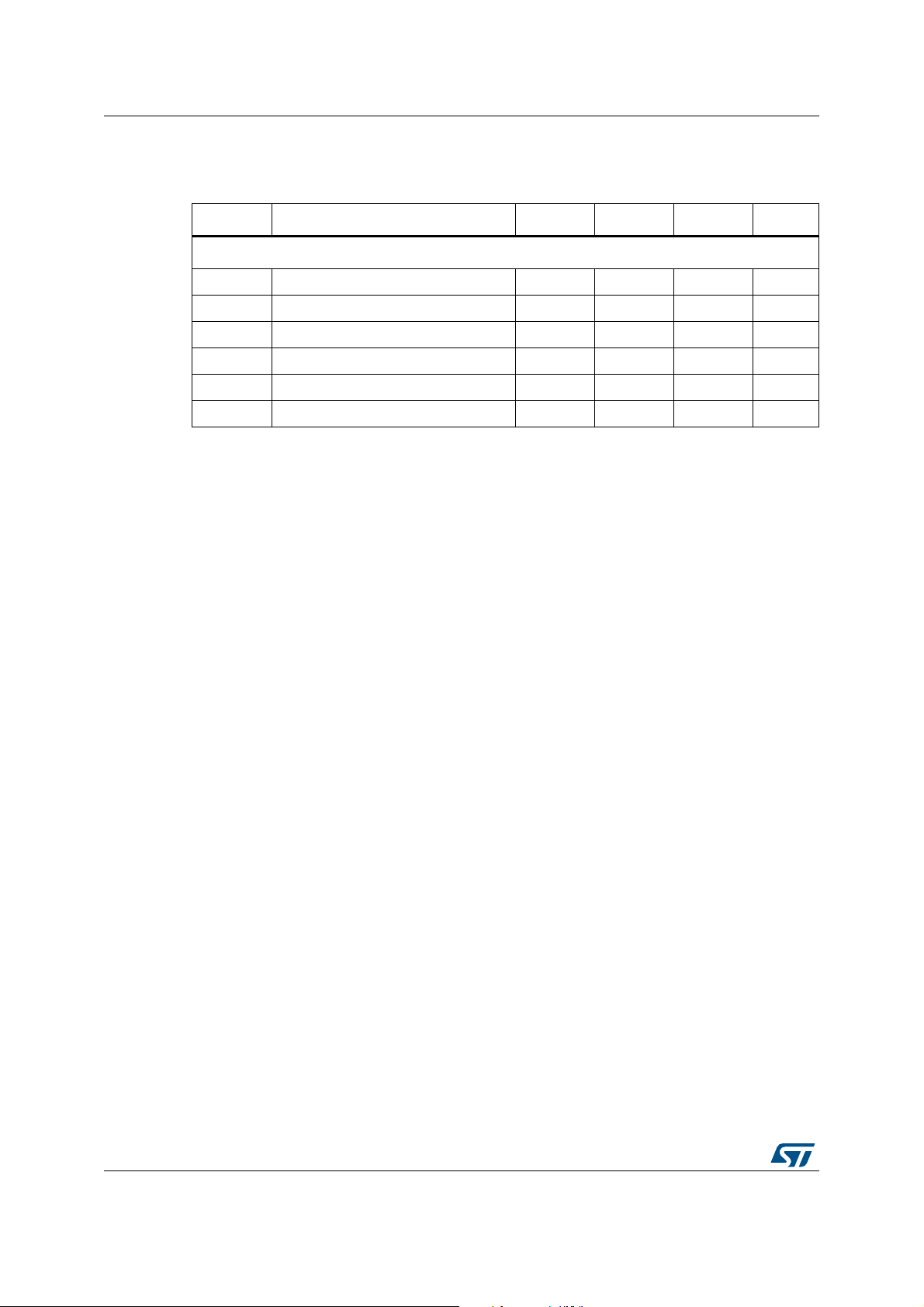
Table 18. Digital I/O electrical characteristics
Symbol Parameter Minimum Typical Maximum Unit
CMOS digital I/O (SDA, SCL, GPIO0 and GPIO1)
V
IL
V
IH
V
OL
V
OH
I
IL
I
IH
Low level input voltage -0.5 - 0.6 V
High level input voltage 1.12 - AVDD+0.5 V
Low level output voltage (8mA load) - - 0.4 V
High level output voltage (8mA load) AVDD-0.4 - - V
Low level input current - - -10 µA
High level input current - - 10 µA
34/79 DocID026171 Rev 6
Page 35
VL6180X Performance specification
4 Performance specification
4.1 Proximity ranging (0 to 100mm)
The following table specifies ranging performance u p to 100mm. Ranging beyon d 100mm is
possible with certain target reflectances and ambient conditions but not guaranteed. These
results are derived from characterization of both typical and corner samples (representative
of worst case process conditions).
Unless specified otherwise, all results were performed at room temperature ( 23°C), nominal
voltage (2.8V) and in the dark. Results are based on the average of 100 measurements for
a 17% reflective target @ 50mm.
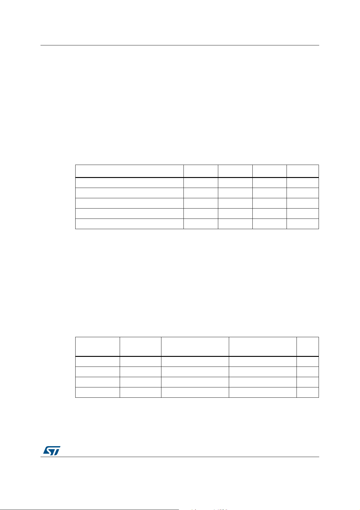
Table 19. Ranging specification
Parameter Min. Typ. Max. Unit
(1)
Noise
Range offset error
Temperature dependent drift
Voltage dependent drift
Convergence time
1. Maximum standard deviation of 100 measurements
2. Maximum offset drift after 3 reflow cycles. This error can be removed by re-calibration in the final system
3. Tested over optimum operating temperature range (see Table 16.: Normal operating conditions)
4. Tested over optimum operating voltage range (see Table 16.: Normal operating conditions)
5. Based on a 3% reflective target @ 100 mm
(2)
(3)
(4)
(5)
- - 2.0 mm
--13mm
-915mm
-35mm
--15ms
4.1.1 Max range vs. ambient light level
The data shown in this section is worst case data for reference only.
Table 20 shows the worst case maximum range achievable under different ambient light
conditions
.
Table 20. Worst case max range vs. ambient 0 to 100mm
Target
reflectance
3% > 100 > 80 > 40 mm
5% > 100 > 90 > 45 mm
17% > 100 > 100 > 60 mm
88% > 100 > 100 > 70 mm
1. Tested in an integrating sphere (repeatable lab test, not representative of real world ambient light) at 1
kLux and 5 kLux (halogen light source) using 80 x 80 mm targets. Due to high IR content, 5 kLux halogen
light approximates to 10 kLux to 15 kLux natural sunlight.
2. SNR limit of 0.1 applied. Note: maximum range could be increased by reducing the SNR limit to 0.06
3. Also applicable to lighting conditions with low IR content e.g typical office fluorescent lighting
In the dark
Worst case indoor light
(3)
(1 kLux diffuse halogen)
DocID026171 Rev 6 35/79
(1)(2)
High ambient light
(5 kLux diffuse halogen)
Unit
78
Page 36
Performance specification VL6180X
4.2 ALS performance
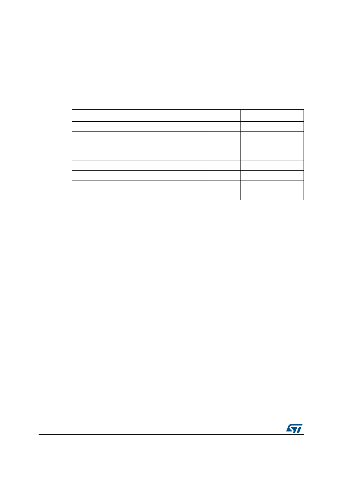
The following table specifies ALS performance. These results are derived from
characterization of typical samples (without cover glass). Unless specified otherwise, all
tests were performed at room temperature (23°C), nominal voltage (2.8V) and using a
halogen light source.
Table 21. ALS performance
Parameter Min. Typ. Max. Unit
ALS sensitivity
Angular response
(1)
(2)
Spectral response - photopic - Dynamic Range
Linearity error (1 to 300 lux)
Linearity error (300 to 7500 lux)
(3)
(4)
(4)
Gain error (@ gain 20) - - 1 %
Gain error (gains 1 to 10) - - 7 %
1. 535nm LED @ 1 kLux. Measured @ gain 20.
2. Half angle. 40% transmission.
3. Minimum of one count at gain 40 and 400 ms ALS integration time.
4. Test conditions: -10°C to +60°C; analog gains 1 to 20
0.28 0.32 0.36 Lux/count
- 42 - degrees
0.002 - 20971 Lux
--5%
--10%
36/79 DocID026171 Rev 6
Page 37
VL6180X I2C control interface
12
7
8
As/Am
Start condition
Stop condition
SDA
SCL
Acknowledge
P
S
3 4 56
Address or data byte
MSB LSB
MSBit
LSBit
0101001R/W
Sensor acknowledges
Acknowledge from sensor
S AsADDRESS[7:0] AsINDEX[15:8] INDEX[7:0] As DATA[7:0] As P
0x52 (write)
Start
Stop
valid address
5 I2C control interface
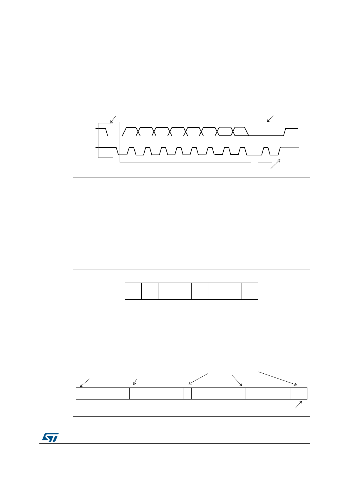
The VL6180X is controlled over an I2C interface. The default I2C address is 0x29 (7-bit).
This section describes the I
2
C protocol.
Figure 21. Serial interface data transfer protocol
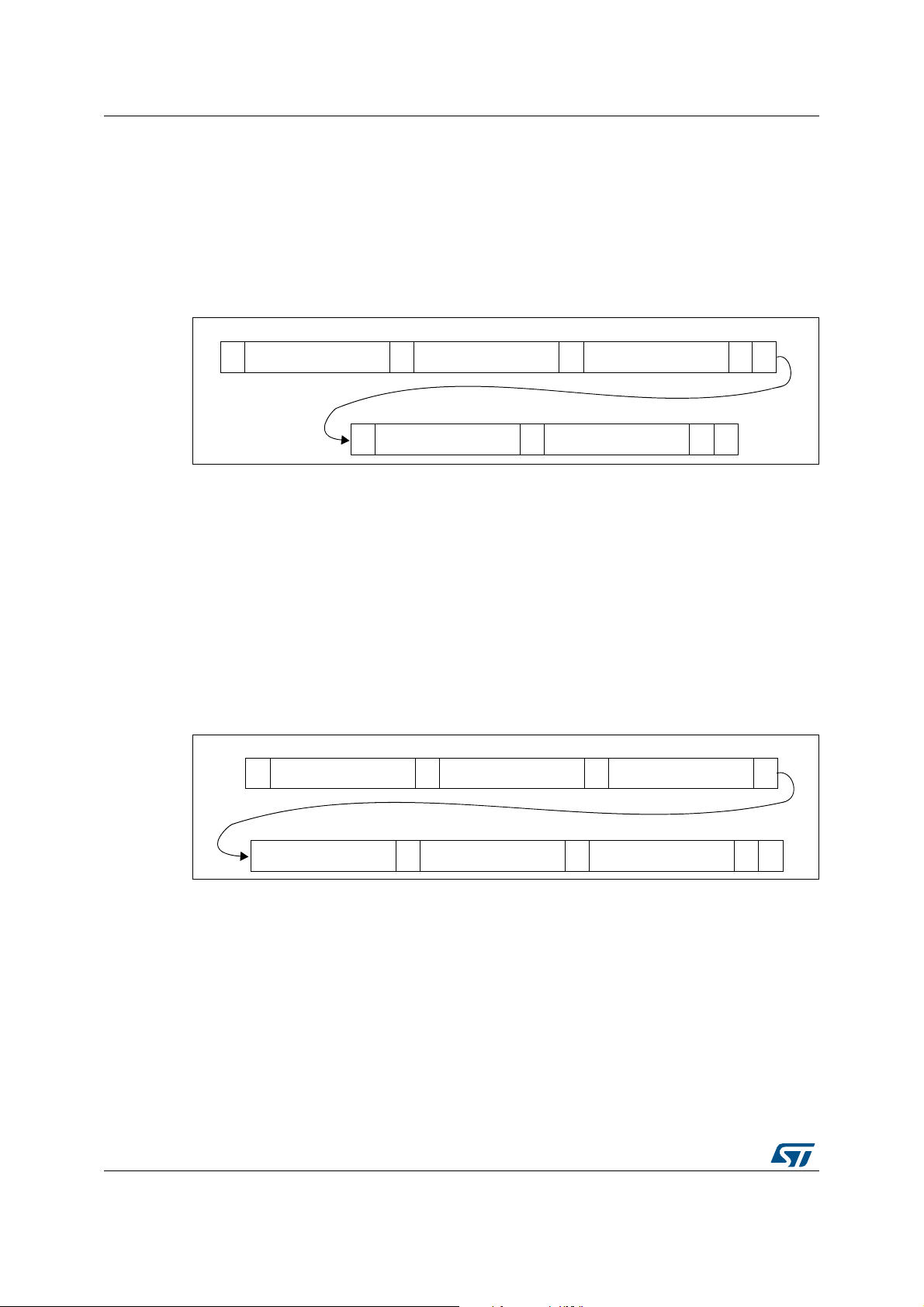
Information is packed in 8-bit packet s (bytes) always followed by an ackn owledge bit, As for
sensor acknowledge and Am for master acknowledge. The internal data is produced by
sampling SDA at a rising edge of SCL. The external data must be stable during the high
period of SCL. The exceptions to this are start (S) or stop (P) conditions when SDA falls or
rises respectively, while SCL is high.
A message contains a series of byte s preceded b y a st art condition an d followed by either a
stop or repeated start (another start condition but without a preceding stop condition)
followed by another message. The first byte contains the device address (0x52) and also
specifies the data direction. If the least significant bit is low (0x52) the message is a master
write to the slave. If the lsb is set (0x53) then the message is a master read from the slave.
Figure 22. I
2
C device address
All serial interface communications with the sensor must begin with a start condition. The
sensor acknowledges the receipt of a valid address by driving the SDA wire low. The state
of the read/write bit (lsb of the address byte) is stored and the next byte of data, sampled
from SDA, can be interpreted. During a write sequence the second and third bytes received
provide a 16-bit index which points to one of the internal 8-bit registers.
Figure 23. Single location, single write)
DocID026171 Rev 6 37/79
78
Page 38
I2C control interface VL6180X
S As
ADDRESS[7:0]
As
INDEX[15:8]
INDEX[7:0]
As P
0x52 (write)
S As
ADDRESS[7:0]
Am
DATA[7:0]
P
0x53 (read)
S As
ADDRESS[7:0]
As
INDEX[15:8]
INDEX[7:0]
As
0x52 (write)
PAs
DATA[7:0]
As
DATA[7:0]
As
DATA[7:0]
As data is received by the slave it is written bit by bit to a serial/parallel re gister. Af ter each
data byte has been received by the slave, an acknowledge is generated, the data is then
stored in the internal register addressed by the current index.
During a read message, the contents of the register addressed by the curren t index is read
out in the byte following the device address byte. The contents of this register are para llel
loaded into the serial/parallel register and clocked out of the device by the falling edge of
SCL.
Figure 24. Single location, single read
At the end of each byte, in both read and write message sequences, an acknowledge is
issued by the receiving device (that is, the sensor for a write and the master for a read).
A message can only be terminated by the bus master, either by issuing a stop condition or
by a negative acknowledge (that is, not pulling the SDA line low) after reading a complete
byte during a read operation.
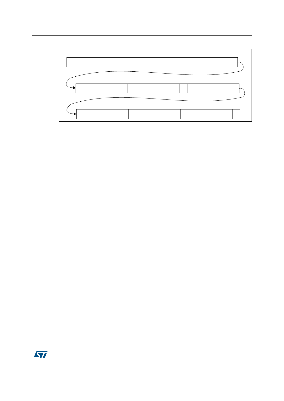
The interface also supports auto-increment indexing. After the first data byte has been
transferred, the index is automatically incremented by 1. The master can therefore send
data bytes continuously to the slave until the slave fails to provide an acknowledge or the
master terminates the write communication with a stop condition. If the auto-increment
feature is used the master does not have to send address indexes to accompany the data
bytes.
Figure 25. Multiple location write
38/79 DocID026171 Rev 6
Page 39
VL6180X I2C control interface
S As
ADDRESS[7:0]
As
INDEX[15:8] INDEX[7:0]
As P
0x52 (write)
S As
ADDRESS[7:0]
Am
DATA[7:0]
P
0x53 (read)
Am
DATA[7:0]
Am
DATA[7:0]
Am
DATA[7:0]
Am
DATA[7:0]
Figure 26. Multiple location read
DocID026171 Rev 6 39/79
78
Page 40
Device registers VL6180X
6 Device registers
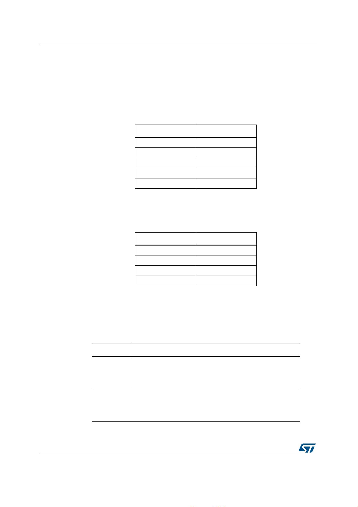
This section describes in detail all user accessible device registers. Registers are grouped
by function as shown in Table 22. to make them easier to read but also to simplify multi-byte
read/write I
each register which denotes the register value in software standby.
Note that registers can be 8-,16- or 32-bit. Multi-byte registers are always addressed in
ascending order with MSB first as shown in Table 23.
2
C accesses (burst mode). More details in Section 5. Reset values are given for
Table 22. Register groups
Register group Address range
IDENTIFICATION 0x00 - 0x0F
SYSTEM SETUP 0x10 - 0x17
RANGE SETUP 0x18 - 0x37
ALS SETUP 0x38 - 0x40
RESULTS 0x4D - 0x80
Table 23. 32-bit register example
Register address Byte
Address MSB
Address + 1 ..
Address + 2 ..
Address + 3 LSB
6.1 Register encoding formats
Some registers are encoded to allow rational numbers to be expressed efficiently. Table 24
gives an explanation of 9.7 and 4.4 encoding formats.
Format Description
4.4
9.7
Table 24. 9.7 and 4.4 register formats
8 bits = 4 integer bits + 4 fractional bits (stored as 1 byte)
Encoding example: the value 4.2 is multiplied by 16 (2
and stored as 67 decimal.
Decoding example: 67 is divided by 16 = 4.19.
16 bits = 9 integer bits + 7 fractional bits (stored over 2 bytes)
Encoding example: the value 4.2 is multiplied by 128 (2
and stored as 537 decimal.
Decoding example: 537 is divided by 128 = 4.19.
4
) rounded
7
) rounded
40/79 DocID026171 Rev 6
Page 41
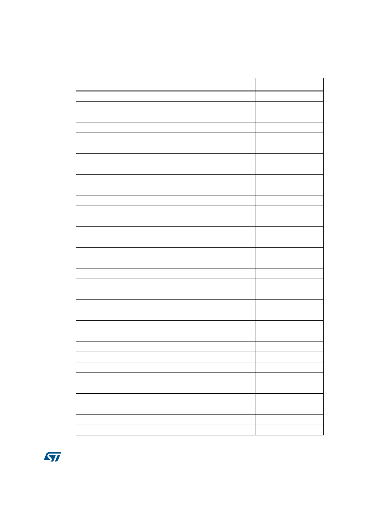
VL6180X Device registers
Table 25. Register summary
Offset Register name Reference
0x000 IDENTIFICATION__MODEL_ID Section 6.2.1 on page 43
0x001 IDENTIFICATION__MODEL_REV_MAJOR Section 6.2.2 on page 43
0x002 IDENTIFICATION__MODEL_REV_MINOR Section 6.2.3 on page 43
0x003 IDENTIFICATION__MODULE_REV_MAJOR Section 6.2.4 on page 44
0x004 IDENTIFICATION__MODULE_REV_MINOR Section 6.2.5 on page 44
0x006 IDENTIFICATION__DATE_HI Section 6.2.6 on page 44
0x007 IDENTIFICATION__DATE_LO Section 6.2.7 on page 45
0x008:0x009 IDENTIFICATION__TIME Section 6.2.8 on page 45
0x010 SYSTEM__MODE_GPIO0 Section 6.2.9 on page 46
0x011 SYSTEM__MODE_GPIO1 Section 6.2.10 on page 47
0x012 SYSTEM__HISTORY_CTRL Section 6.2.11 on page 48
0x014 SYSTEM__INTERRUPT_CONFIG_GPIO Section 6.2.12 on page 49
0x015 SYSTEM__INTERRUPT_CLEAR Section 6.2.13 on page 49
0x016 SYSTEM__FRESH_OUT_OF_RESET Section 6.2.14 on page 50
0x017 SYSTEM__GROUPED_PARAMETER_HOLD Section 6.2.15 on page 50
0x018 SYSRANGE__START Section 6.2.16 on page 51
0x019 SYSRANGE__THRESH_HIGH Section 6.2.17 on page 51
0x01A SYSRANGE__THRESH_LOW Section 6.2.18 on page 52
0x01B SYSRANGE__INTERMEASUREMENT_PERIOD Section 6.2.19 on page 52
0x01C SYSRANGE__MAX_CONVERGENCE_TIME Section 6.2.20 on page 52
0x01E SYSRANGE__CROSSTALK_COMPENSATION_RATE Section 6.2.21 on page 53
0x021 SYSRANGE__CROSSTALK_VALID_HEIGHT Section 6.2.22 on page 53
0x022 SYSRANGE__EARLY_CONVERGENCE_ESTIMATE Section 6.2.23 on page 53
0x024 SYSRANGE__PART_TO_PART_RANGE_OFFSET Section 6.2.24 on page 54
0x025 SYSRANGE__RANGE_IGNORE_VALID_HEIGHT Section 6.2.25 on page 54
0x026 SYSRANGE__RANGE_IGNORE_THRESHOLD Section 6.2.26 on page 54
0x02C SYSRANGE__MAX_AMBIENT_LEVEL_MULT Section 6.2.27 on page 55
0x02D SYSRANGE__RANGE_CHECK_ENABLES Section 6.2.27 on page 55
0x02E SYSRANGE__VHV_RECALIBRATE Section 6.2.29 on page 56
0x031 SYSRANGE__VHV_REPEAT_RATE Section 6.2.30 on page 56
0x038 SYSALS__START Section 6.2.31 on page 57
0x03A SYSALS__THRESH_HIGH Section 6.2.32 on page 57
0x03C SYSALS__THRESH_LOW Section 6.2.33 on page 58
DocID026171 Rev 6 41/79
78
Page 42
Device registers VL6180X
Table 25. Register summary (continued)
Offset Register name Reference
0x03E SYSALS__INTERMEASUREMENT_PERIOD Section 6.2.34 on page 58
0x03F SYSALS__ANALOGUE_GAIN Section 6.2.35 on page 59
0x040 SYSALS__INTEGRATION_PERIOD Section 6.2.36 on page 59
0x04D RESULT__RANGE_STATUS Section 6.2.37 on page 60
0x04E RESULT__ALS_STATUS Section 6.2.38 on page 61
0x04F RESULT__INTERRUPT_STATUS_GPIO Section 6.2.39 on page 62
0x050 RESULT__ALS_VAL Section 6.2.40 on page 62
0x052:0x060
(0x2)
0x062 RESULT__RANGE_VAL Section 6.2.42 on page 64
0x064 RESULT__RANGE_RAW Section 6.2.43 on page 64
0x066 RESULT__RANGE_RETURN_RATE Section 6.2.44 on page 64
0x068 RESULT__RANGE_REFERENCE_RATE Section 6.2.45 on page 65
0x06C RESULT__RANGE_RETURN_SIGNAL_COUNT Section 6.2.46 on page 65
0x070 RESULT__RANGE_REFERENCE_SIGNAL_COUNT Section 6.2.47 on page 66
0x074 RESULT__RANGE_RETURN_AMB_COUNT Section 6.2.48 on page 66
0x078 RESULT__RANGE_REFERENCE_AMB_COUNT Section 6.2.49 on page 66
0x07C RESULT__RANGE_RETURN_CONV_TIME Section 6.2.50 on page 67
0x080 RESULT__RANGE_REFERENCE_CONV_TIME Section 6.2.51 on page 67
0x10A READOUT__AVERAGING_SAMPLE_PERIOD Section 6.2.52 on page 67
0x119 FIRMWARE__BOOTUP Section 6.2.52 on page 67
0x120 FIRMWARE__RESULT_SCALER Section 6.2.53 on page 68
0x212 I2C_SLAVE__DEVICE_ADDRESS Section 6.2.55 on page 68
0x2A3 INTERLEAVED_MODE__ENABLE Section 6.2.56 on page 69
RESULT__HISTORY_BUFFER_x Section 6.2.41 on page 63
42/79 DocID026171 Rev 6
Page 43
VL6180X Device registers
6.2 Register descriptions
6.2.1 IDENTIFICATION__MODEL_ID
76543210
identification__model_id
R/W
Address: 0x000
Type: R/W
Reset: 0xB4
Description:
[7:0] identification__model_id: Device model identification number. 0xB4 = VL6180X
6.2.2 IDENTIFICATION__MODEL_REV_MAJOR
76543210
RESERVED identification__model_rev_major
RR/W
Address: 0x001
Type: R/W
Reset: 0x1, register default overwritten at boot-up by NVM contents.
Description:
[2:0] identification__model_rev_major: Revision identifier of the Device for major change.
6.2.3 IDENTIFICATION__MODEL_REV_MINOR
76543210
RESERVED identification__model_rev_minor
RR/W
Address: 0x002
Type: R/W
Reset: 0x3, register default overwritten at boot-up by NVM contents.
Description:
[2:0] identification__model_rev_minor: Revision identifi er of the Device for minor change.
IDENTIFICATION__MODEL_REV_MINOR = 3 for latest ROM revision
DocID026171 Rev 6 43/79
78
Page 44
Device registers VL6180X
6.2.4 IDENTIFICATION__MODULE_REV_MAJOR
76543210
RESERVED identification__module_rev_major
RR/W
Address: 0x003
Type: R/W
Reset: 0x1, register default overwritten at boot-up by NVM contents.
Description:
[2:0] identification__module_rev_major: Revision identifier of the Module Package for major change.
Used to store NVM content version. Contact ST for current information.
6.2.5 IDENTIFICATION__MODULE_REV_MINOR
76543210
RESERVED identification__module_rev_minor
RR/W
Address: 0x004
Type: R/W
Reset: 0x2, register default overwritten at boot-up by NVM contents.
Description:
[2:0] identification__module_rev_minor: Revision identifier of the Module Package for minor change.
Used to store NVM content version. Contact ST for current information.
6.2.6 IDENTIFICATION__DATE_HI
76543210
identification__year identification__month
R/W R/W
Address: 0x006
Type: R/W
Reset: 0xYY, register default overwritten at boot-up by NVM contents.
Description: Part of the register set that can be used to uniquely identify a module.
[7:4] identification__year: Last digit of manufacturing year (bits[3:0]).
[3:0] identification__month: Manufacturing month (bits[3:0]).
44/79 DocID026171 Rev 6
Page 45
VL6180X Device registers
6.2.7 IDENTIFICATION__DATE_LO
76543210
identification__day identification__phase
R/W R/W
Address: 0x007
Type: R/W
Reset: 0xYY, register default overwritten at boot-up by NVM contents.
Description: Part of the register set that can be used to uniquely identify a module.
[7:3] identification__day: Manufacturing day (bits[4:0]).
[2:0] identification__phase: Manufacturing phase identification (bits[2:0]).
6.2.8 IDENTIFICATION__TIME
1514131211109876543210
identification__time
R/W
Address: 0x008:0x009
Type: R/W
Reset: 0xYYYY, register default overwritten at boot-up by NVM contents.
Description: Part of the register set that can be used to uniquely identify a module.
[15:0] identification__time: Time since midnight (in seconds) = register_value * 2
DocID026171 Rev 6 45/79
78
Page 46
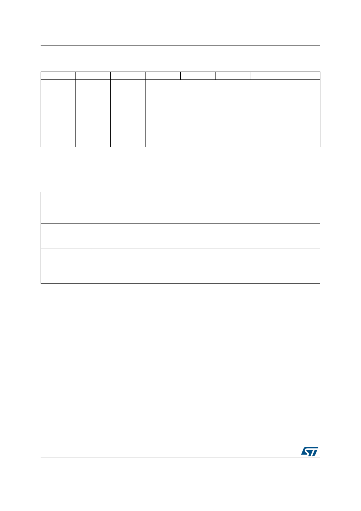
Device registers VL6180X
6.2.9 SYSTEM__MODE_GPIO0
76543210
RESERVED
system__gpio0_is_xshutdown
system__gpio0_polarity
R R/W R/W R/W R/W
system__gpio0_select
Address: 0x010
Type: R/W
Reset: 0x60
Description:
[6] system__gpio0_is_xshutdown: Priority mode - when enabled, other bits of the register are
ignored. GPIO0 is main XSHUTDOWN input.
0: Disabled
1: Enabled - GPIO0 is main XSHUTDOWN input.
[5] system__gpio0_polarity: Signal Polarity Selection.
0: Active-low
1: Active-high
[4:1] system__gpio0_select: Functional configuration options.
0000: OFF (Hi-Z)
1000: GPIO Interrupt output
[0] Reserved. Write 0.
RESERVED
46/79 DocID026171 Rev 6
Page 47
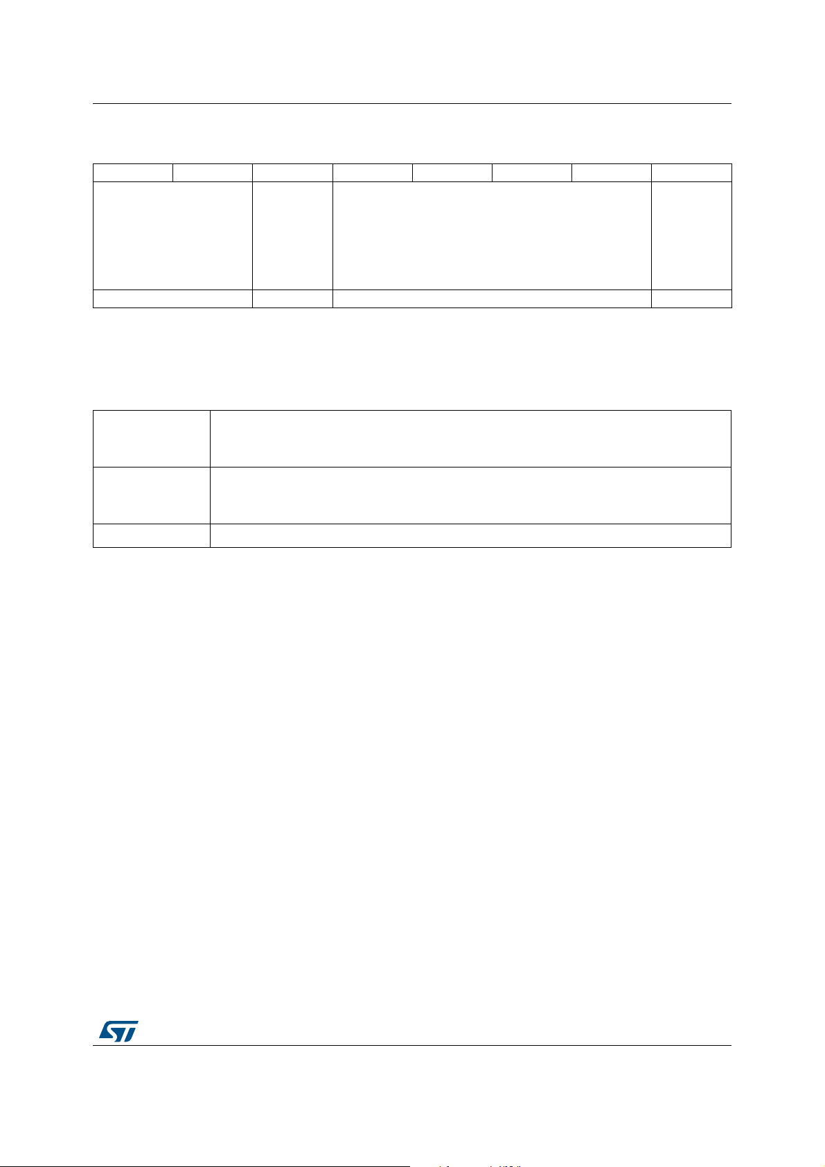
VL6180X Device registers
6.2.10 SYSTEM__MODE_GPIO1
76543210
RESERVED
R R/W R/W R/W
Address: 0x011
Type: R/W
Reset: 0x20
Description:
[5] system__gpio1_polarity: Signal Polarity Selection.
0: Active-low
1: Active-high
[4:1] system__gpio1_select: Functional configuration options.
0000: OFF (Hi-Z)
1000: GPIO Interrupt output
[0] Reserved. Write 0.
RESERVED
system__gpio1_polarity
system__gpio1_select
DocID026171 Rev 6 47/79
78
Page 48
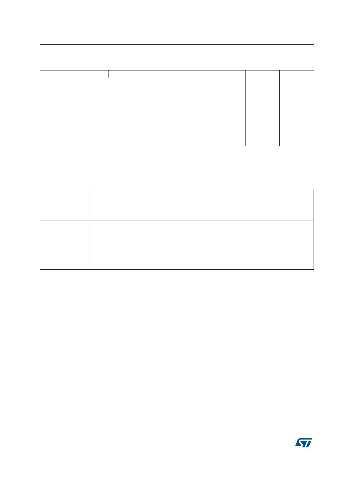
Device registers VL6180X
6.2.11 SYSTEM__HISTORY_CTRL
76543210
RESERVED
Address: 0x012
Type: R/W
Reset: 0x0
Description:
[2] system__history_buffer_clear: User-command to clear history (FW will auto-clear this bit when
clear has completed).
0: Disabled
1: Clear all history buffers
[1] system__history_buffer_mode: Select mode buffer results for:
0: Ranging (stores the last 8 ranging values (8-b it)
1: ALS (stores the last 8 ALS values (16-bit)
[0] system__history_buffer_enable: Enable History buffering.
0: Disabled
1: Enabled
system__history_buffer_clear
R R/W R/W R/W
system__history_buffer_mode
system__history_buffer_enable
48/79 DocID026171 Rev 6
Page 49
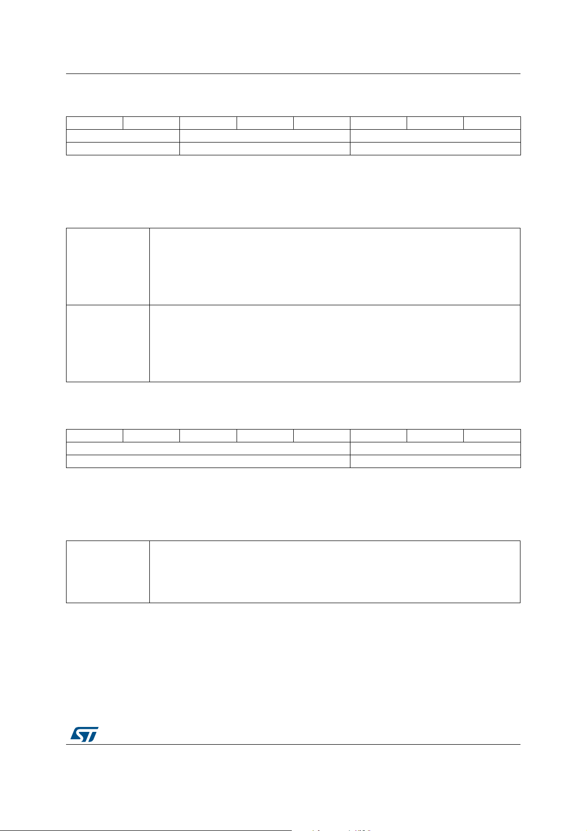
VL6180X Device registers
6.2.12 SYSTEM__INTERRUPT_CONFIG_GPIO
76543210
RESERVED als_int_mode range_int_mode
RR/W R/W
Address: 0x014
Type: R/W
Reset: 0x0
Description:
[5:3] als_int_mode: Interrupt mode source for ALS readings:
0: Disabled
1: Level Low (value < thresh_low)
2: Level High (value > thresh_high)
3: Out Of Window (value < thresh_low OR value > thresh_high)
4: New sample ready
[2:0] range_int_mode: Interrupt mode source for Range readings:
0: Disabled
1: Level Low (value < thresh_low)
2: Level High (value > thresh_high)
3: Out Of Window (value < thresh_low OR value > thresh_high)
4: New sample ready
6.2.13 SYSTEM__INTERRUPT_CLEAR
76543210
RESERVED int_clear_sig
RR/W
Address: 0x015
Type: R/W
Reset: 0x0
Description:
[2:0] int_clear_sig: Interrupt clear bits. Writing a 1 to each bit will clear the intended interrupt.
Bit [0] - Clear Range Int
Bit [1] - Clear ALS Int
Bit [2] - Clear Error Int.
DocID026171 Rev 6 49/79
78
Page 50
Device registers VL6180X
6.2.14 SYSTEM__FRESH_OUT_OF_RESET
76543210
RESERVED
RR/W
Address: 0x016
Type: R/W
Reset: 0x1
Description:
[0] fresh_out_of_reset: Fresh out of reset bit, default of 1, user can set this to 0 after initial boot and
can therefore use this to check for a reset condition
6.2.15 SYSTEM__GROUPED_PARAMETER_HOLD
76543210
RESERVED
RR/W
fresh_out_of_reset
grouped_parameter_hold
Address: 0x017
Type: R/W
Reset: 0x0
Description:
[0] grouped_parameter_hold: Flag set over I2C to indicate that data is being updated
0: Data is stable - FW is safe to copy
1: Data being updated - FW not safe to copy
Usage: set to 0x01 first, write any of the registers listed below, then set to 0x00 so that the
settings are used by the firmware at the start of the next measurement.
SYSTEM__INTERRUPT_CONFIG_GPIO
SYSRANGE__THRESH_HIGH
SYSRANGE__THRESH_LOW
SYSALS__INTEGRATION_PERIOD
SYSALS__ANALOGUE_GAIN
SYSALS__THRESH_HIGH
SYSALS__THRESH_LOW
50/79 DocID026171 Rev 6
Page 51
VL6180X Device registers
6.2.16 SYSRANGE__START
76543210
RESERVED
sysrange__mode_select
RR/WR/W
Address: 0x018
Type: R/W
Reset: 0x0
Description:
[1] sysrange__mode_select: Device Mode select
0: Ranging Mode Single-Shot
1: Ranging Mode Continuous
[0] sysrange__startstop: StartStop trigger based on current mode and system configuration of
device_ready. FW clears register automatically.
Setting this bit to 1 in single-shot mode starts a single measurement.
Setting this bit to 1 in continuous mode will either start continuous operation (if stopped) or halt
continuous operation (if started).
This bit is auto-cleared in both modes of operation.
sysrange__startstop
6.2.17 SYSRANGE__THRESH_HIGH
76543210
sysrange__thresh_high
R/W
Address: 0x019
Type: R/W
Reset: 0xFF
Description:
[7:0] sysrange__thresh_high: High Threshold value for ranging comparison. Range 0-255mm.
DocID026171 Rev 6 51/79
78
Page 52
Device registers VL6180X
6.2.18 SYSRANGE__THRESH_LOW
76543210
sysrange__thresh_low
R/W
Address: 0x01A
Type: R/W
Reset: 0x0
Description:
[7:0] sysrange__thresh_low: Low Threshold value for ranging comparison. Range 0-255mm.
6.2.19 SYSRANGE__INTERMEASUREMENT_PERIOD
76543210
sysrange__intermeasurement_period
R/W
Address: 0x01B
Type: R/W
Reset: 0xFF
Description:
[7:0] sysrange__intermeasurement_period: Time delay between measurements in Ranging
continuous mode. Range 0-254 (0 = 10ms). Step size = 10ms.
6.2.20 SYSRANGE__MAX_CONVERGENCE_TIME
76543210
RESERVED sysrange__max_convergence_time
RR/W
Address: 0x01C
Type: R/W
Reset: 0x31
Description:
[5:0] sysrange__max_convergence_time: Maximum time to run measurement in Ranging modes.
Range 1 - 63 ms (1 code = 1 ms); Measurement aborted when limit reached to aid power
reduction. For example, 0x01 = 1ms, 0x0a = 10ms.
Note: Effective max_convergence_time depends on readout_averaging_sample_period
setting.
52/79 DocID026171 Rev 6
Page 53
VL6180X Device registers
6.2.21 SYSRANGE__CROSSTALK_COMPENSATION_RATE
1514131211109876543210
sysrange__crosstalk_compensation_rate
R/W
Address: 0x01E
Type: R/W
Reset: 0x0
Description:
[15:0] sysrange__crosstalk_compensation_rate: User-controlled crosstalk compensation in Mcps (9.7
format).
6.2.22 SYSRANGE__CROSSTALK_VALID_HEIGHT
76543210
sysrange__crosstalk_valid_height
R/W
Address: 0x021
Type: R/W
Reset: 0x14
Description:
[7:0] sysrange__crosstalk_valid_height: Minimum range value in mm to qua lify for crosstalk
compensation.
6.2.23 SYSRANGE__EARLY_CONVERGENCE_ESTIMATE
1514131211109876543210
Address: 0x022
Type: R/W
Reset: 0x0
Description:
sysrange__early_convergence_estimate
R/W
[15:0] FW carries out an estimate of convergence rate 0.5ms into each new range measurement. If
convergence rate is below user input value, the operation aborts to save power.
Note: This register must be configured otherwise ECE should be disabled via
SYSRANGE__RANGE_CHECK_ENABLES.
DocID026171 Rev 6 53/79
78
Page 54
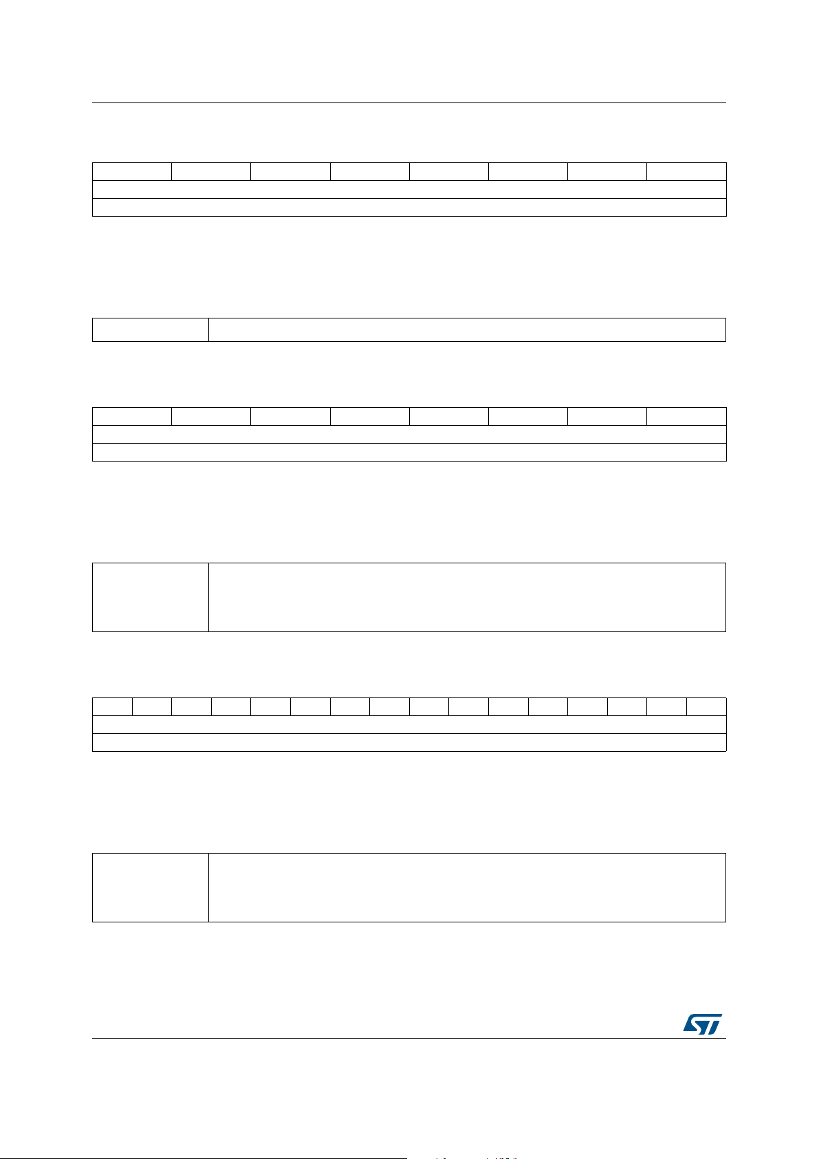
Device registers VL6180X
6.2.24 SYSRANGE__PART_TO_PART_RANGE_OFFSET
76543210
sysrange__part_to_part_range_offset
R/W
Address: 0x024
Type: R/W
Reset: 0xYY, register default overwritten at boot-up by NVM contents.
Description:
[7:0] sysrange__part_to_part_range_offset: 2s complement format.
6.2.25 SYSRANGE__RANGE_IGNORE_VALID_HEIGHT
76543210
sysrange__range_ignore_valid_height
R/W
Address: 0x025
Type: R/W
Reset: 0x0, register default overwritten at boot-up by NVM contents.
Description:
[7:0] sysrange__range_ignore_valid_height: Range below which ignore threshold is applied. Aim is
to ignore the cover glass i.e. low signal rate at near distance. Should not be applied to low
reflectance target at far distance. Range in mm.
Note: It is recommended to set this register to 255 if the range ignore feature is used.
6.2.26 SYSRANGE__RANGE_IGNORE_THRESHOLD
1514131211109876543210
Address: 0x026
Type: R/W
Reset: 0xYY
Description:
sysrange__range_ignore_threshold
R/W
[15:0] sysrange__range_ignore_threshold: User configurable min threshold signal return rate. Used
to filter out ranging due to cover glass when there is no target above the device. Mcps 9.7
format.
Note: Register must be initialized if this feature is used.
54/79 DocID026171 Rev 6
Page 55
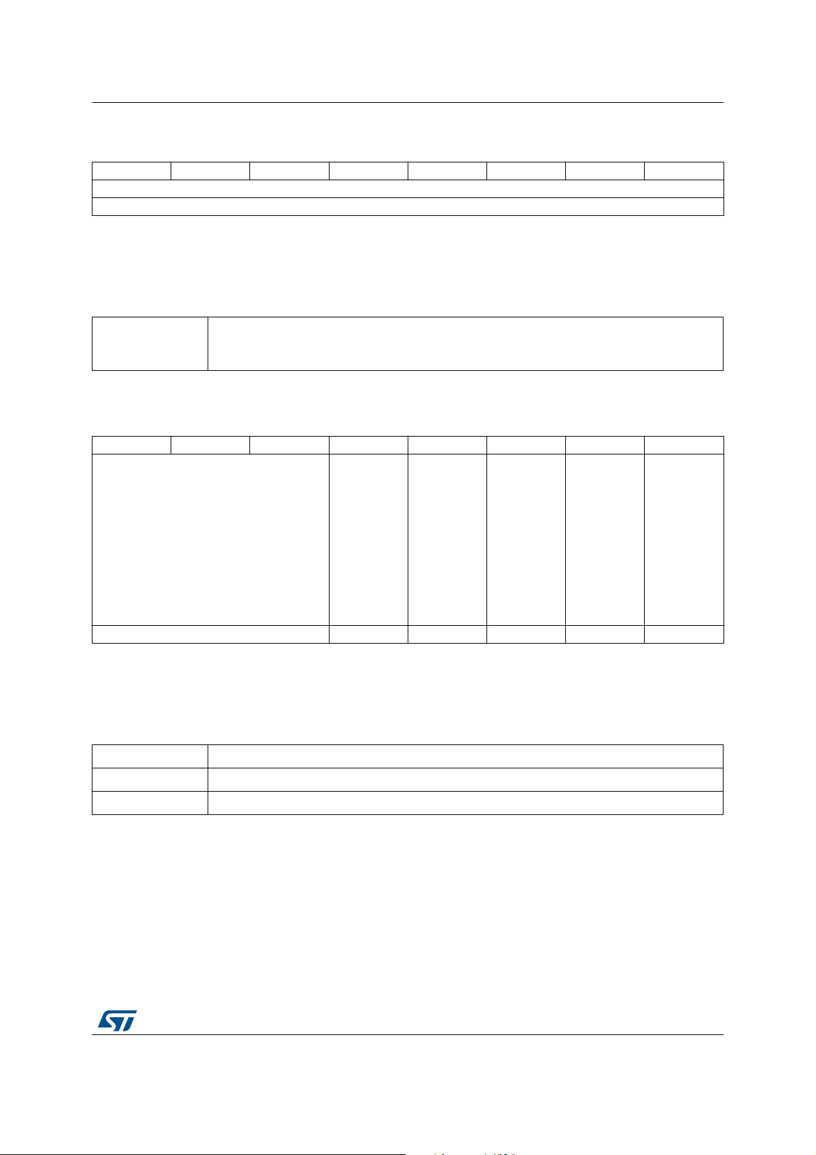
VL6180X Device registers
6.2.27 SYSRANGE__MAX_AMBIENT_LEVEL_MULT
76543210
sysrange__max_ambient_level_mult
R/W
Address: 0x02C
Type: R/W
Reset: 0xA0, register default overwritten at boot-up by NVM contents.
Description:
[7:0] sysrange__max_ambient_level_mult: User input value to multiply return_signal_count for
AMB:signal ratio check. If (amb counts * 6) > return_signal_count * mu lt then abandon
measurement due to high ambient (4.4 format).
6.2.28 SYSRANGE__RANGE_CHECK_ENABLES
76543210
0
RESERVED
sysrange__signal_to_noise_enable
RR/WR/WRR/WR/W
0
Address: 0x02D
Type: R/W
Reset: 0x11, register default overwritten at boot-up by NVM contents.
Description:
[4] sysrange__signal_to_noise_enable: Measurement enable/disable
[1] sysrange__range_ignore_enable: Measurement enable/disable
[0] sysrange__early_convergence_enable: Measurement enable/disable
sysrange__range_ignore_enable
sysrange__early_convergence_enable
DocID026171 Rev 6 55/79
78
Page 56
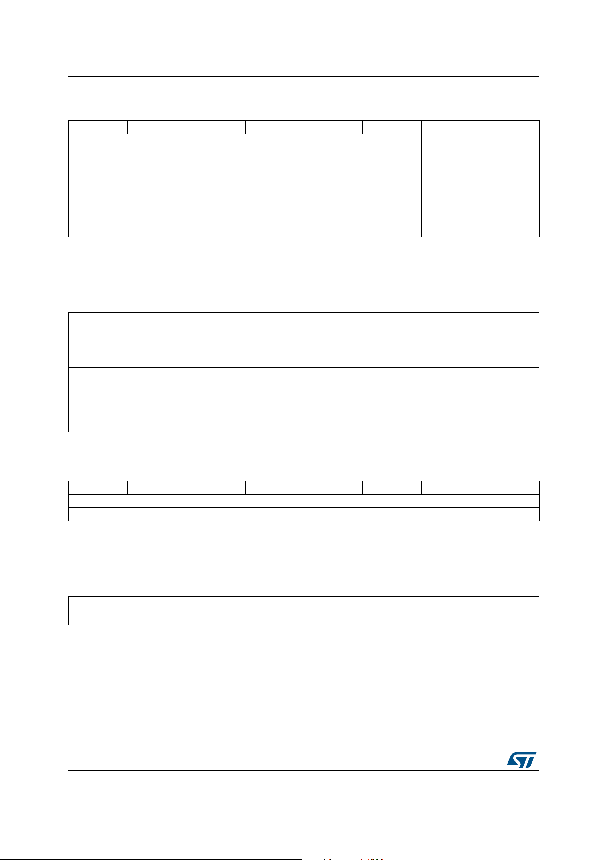
Device registers VL6180X
6.2.29 SYSRANGE__VHV_RECALIBRATE
76543210
RESERVED
sysrange__vhv_status
RR/WR/W
Address: 0x02E
Type: R/W
Reset: 0x0
Description:
[1] sysrange__vhv_status: FW controlled status bit showing when FW has completed auto-vhv
process.
0: FW has finished autoVHV operation
1: During autoVHV operation
sysrange__vhv_recalibrate
[0] sysrange__vhv_recalibrate: User-Controlled enable bit to force FW to carry out recalibration of
the VHV setting for sensor array. FW clears bit after operation carried out.
0: Disabled
1: Manual trigger for VHV recalibration. Can only be called when ALS and ranging are in STOP
mode
6.2.30 SYSRANGE__VHV_REPEAT_RATE
76543210
sysrange__vhv_repeate_rate
R/W
Address: 0x031
Type: R/W
Reset: 0x0
Description:
[7:0] sysrange__vhv_repeat_rate: User entered repeat rate of auto VHV task (0 = off, 255 = after
every 255 measurements)
56/79 DocID026171 Rev 6
Page 57
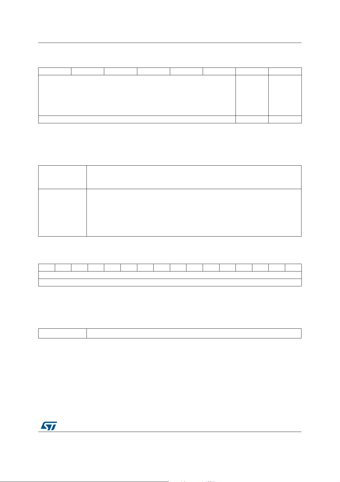
VL6180X Device registers
6.2.31 SYSALS__START
76543210
RESERVED
sysals__mode_select
RR/WR/W
sysals__startstop
Address: 0x038
Type: R/W
Reset: 0x0
Description:
[1] sysals__mode_select: Device Mode select
0: ALS Mode Single-Shot
1: ALS Mode Continuous
[0] sysals__startstop: Start/Stop trigger based on current mode and system configuration of
device_ready. FW clears register automatically.
Setting this bit to 1 in single-shot mode starts a single measurement.
Setting this bit to 1 in continuous mode will either start continuous operation (if stopped) or halt
continuous operation (if started).
This bit is auto-cleared in both modes of operation.
See 6.2.56: INTERLEAVED_MODE__ENABLE for combined ALS and Range operation.
6.2.32 SYSALS__THRESH_HIGH
1514131211109876543210
sysals__thresh_high
R/W
Address: 0x03A
Type: R/W
Reset: 0xFFFF
Description:
[15:0] sysals__thresh_high: Hig h Threshold value for ALS comparison. Range 0-65535 codes.
DocID026171 Rev 6 57/79
78
Page 58
Device registers VL6180X
6.2.33 SYSALS__THRESH_LOW
1514131211109876543210
sysals__thresh_low
R/W
Address: 0x03C
Type: R/W
Reset: 0x0
Description:
[15:0] sysals__thresh_low: Low Threshold value for ALS comparison. Range 0-65535 codes.
6.2.34 SYSALS__INTERMEASUREMENT_PERIOD
76543210
sysals__intermeasurement_period
R/W
Address: 0x03E
Type: R/W
Reset: 0xFF
Description:
[7:0] sysals__intermeasurement_period: Time delay between measurements in ALS continuous
mode. Range 0-254 (0 = 10ms). Step size = 10ms.
58/79 DocID026171 Rev 6
Page 59
VL6180X Device registers
6.2.35 SYSALS__ANALOGUE_GAIN
76543210
RESERVED sysals__analogue_gain_light
RR/W
Address: 0x03F
Type: R/W
Reset: 0x06
Description:
[2:0] sysals__analogue_gain_light: ALS analogue gain (light channel)
0: ALS Gain = 20
1: ALS Gain = 10
2: ALS Gain = 5.0
3: ALS Gain = 2.5
4: ALS Gain = 1.67
5: ALS Gain = 1.25
6: ALS Gain = 1.0
7: ALS Gain = 40
Controls the “light” channel gain.
Note: Upper nibble should be set to 0x4 i.e. For ALS gain of 1.0 write 0x46.
6.2.36 SYSALS__INTEGRATION_PERIOD
1514131211109876543210
Address: 0x040
Type: R/W
Reset: 0x0
Description:
RESERVED sysals__integration_period
RR/W
[8:0] sysals__integration_period: Integration period for ALS mode. 1 code = 1 ms (0 = 1 ms).
Recommended setting is 100 ms (0x63).
DocID026171 Rev 6 59/79
78
Page 60
Device registers VL6180X
6.2.37 RESULT__RANGE_STATUS
76543210
Address: 0x04D
Type: R
Reset: 0x1
Description:
[7:4] result__range_error_code: Specific error codes
0000: No error
0001: VCSEL Continuity Test
0010: VCSEL Watchdog Test
0011: VCSEL Watchdog
0100: PLL1 Lock
0101: PLL2 Lock
0110: Early Convergence Estimate
0111: Max Convergence
1000: No Target Ignore
1001: Not used
1010: Not used
1011: Max Signal To Noise Ratio
1100: Raw Ranging Algo Underflow
1101: Raw Ranging Algo Overflow
1110: Ranging Algo Underflow
1 111: Ranging Algo Overflow
result__range_error_code
result__range_min_threshold_hit
RRRRR
result__range_max_threshold_hit
result__range_measurement_ready
result__range_device_ready
[3] result__range_min_threshold_hit: Legacy register - DO NOT USE
Use instead 6.2.39: RESULT__INTERRUPT_STATUS_GPIO
[2] result__range_max_threshold_hit: Legacy register - DO NOT USE
Use instead 6.2.39: RESULT__INTERRUPT_STATUS_GPIO
[1] result__range_measurement_ready: Legacy register - DO NOT USE
Use instead 6.2.39: RESULT__INTERRUPT_STATUS_GPIO
[0] result__range_device_ready: Device Ready. When set to 1, indicates the device mode and
configuration can be changed and a new start command will be accepted. When 0, indicates
the device is busy.
60/79 DocID026171 Rev 6
Page 61
VL6180X Device registers
6.2.38 RESULT__ALS_STATUS
76543210
Address: 0x04E
Type: R
Reset: 0x1
Description:
[7:4] result__als_error_code: Specific error and debug codes
0000: No error
0001: Overflow error
0002: Underflow error
[3] result__als_min_threshold_hit: Legacy register - DO NOT USE
Use instead 6.2.39: RESULT__INTERRUPT_STATUS_GPIO
[2] result__als_max_threshold_hit: Legacy register - DO NOT USE
Use instead 6.2.39: RESULT__INTERRUPT_STATUS_GPIO
[1] result__als_measurement_ready: Legacy register - DO NOT USE
Use instead 6.2.39: RESULT__INTERRUPT_STATUS_GPIO
[0] result__als_device_ready: Device Ready. When set to 1, indicates the device mode and
configuration can be changed and a new start command will be accepted. When 0 indicates the
device is busy.
result__als_error_code
result__als_min_threshold_hit
RRRRR
result__als_max_threshold_hit
result__als_measurement_ready
result__als_device_ready
DocID026171 Rev 6 61/79
78
Page 62
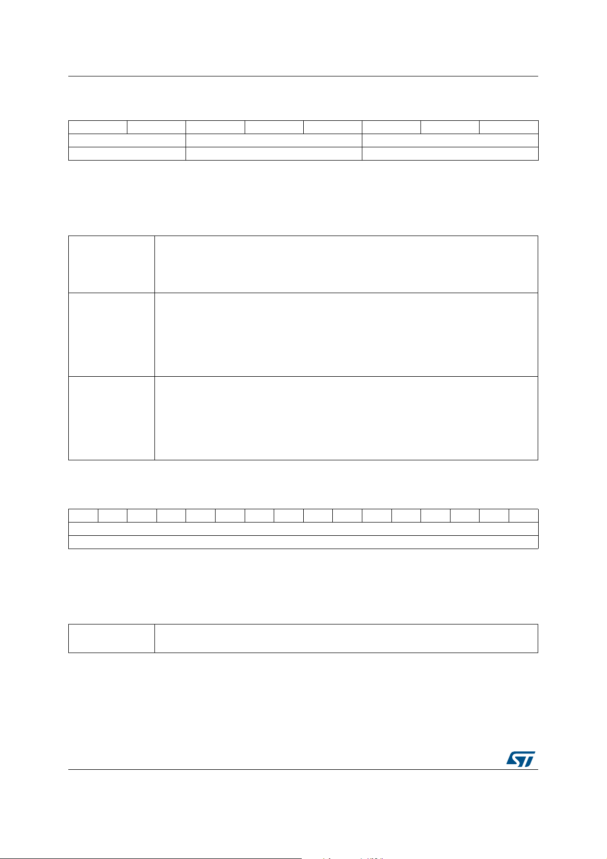
Device registers VL6180X
6.2.39 RESULT__INTERRUPT_STATUS_GPIO
76543210
result_int_error_gpio result_int_als_gpio result_int_range_gpio
RR R
Address: 0x04F
Type: R
Reset: 0x0
Description:
[7:6] result_int_error_gpio: Interrupt bits for Error:
0: No error reported
1: Laser Safety Error
2: PLL error (either PLL1 or PLL2)
[5:3] result_int_als_gpio: Interrupt bits for ALS:
0: No threshold events reported
1: Level Low threshold event
2: Level High threshold event
3: Out Of Window threshold event
4: New Sample Ready threshold event
[2:0] result_int_range_gpio: Interrupt bits for Range:
0: No threshold events reported
1: Level Low threshold event
2: Level High threshold event
3: Out Of Window threshold event
4: New Sample Ready threshold event
6.2.40 RESULT__ALS_VAL
1514131211109876543210
Address: 0x050
Type: R
Reset: 0x0
Description:
result__als_ambient_light
R
[15:0] result__als_ambient_light: 16 Bit ALS count output value. Lux value depends on Gain and
integration settings and calibrated lux/count setting.
62/79 DocID026171 Rev 6
Page 63
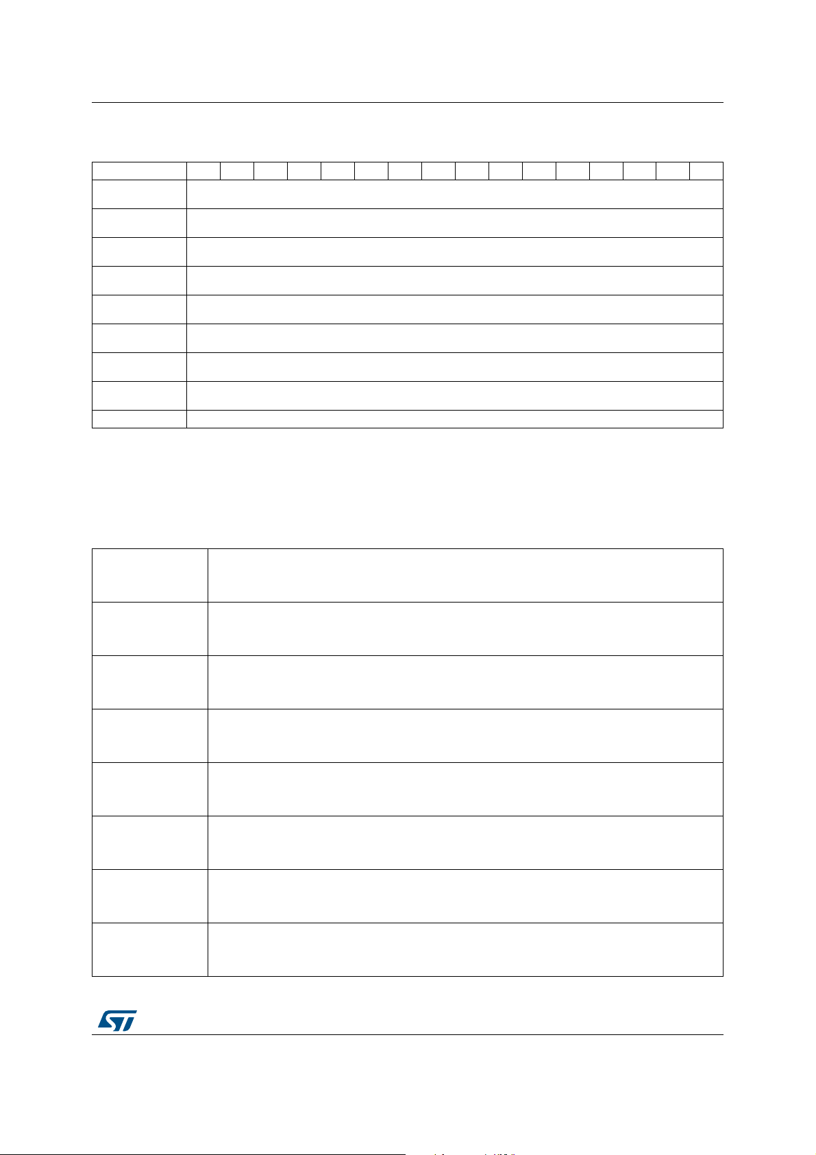
VL6180X Device registers
6.2.41 RESULT__HISTORY_BUFFER_x
1514131211109876543210
RESULT__HISTOR
Y_BUFFER_0
RESULT__HISTOR
Y_BUFFER_1
RESULT__HISTOR
Y_BUFFER_2
RESULT__HISTOR
Y_BUFFER_3
RESULT__HISTOR
Y_BUFFER_4
RESULT__HISTOR
Y_BUFFER_5
RESULT__HISTOR
Y_BUFFER_6
RESULT__HISTOR
Y_BUFFER_7
Address: 0x052 + x * 0x2 (x=0 to 7)
Type: R
result__history_buffer_0
result__history_buffer_1
result__history_buffer_2
result__history_buffer_3
result__history_buffer_4
result__history_buffer_5
result__history_buffer_6
result__history_buffer_7
R
Reset: 0x0
Description: See also 6.2.11: SYSTEM__HISTORY_CTRL
RESULT__HISTOR
Y_BUFFER_0:
[15:0]
RESULT__HISTOR
Y_BUFFER_1:
[15:0]
RESULT__HISTOR
Y_BUFFER_2:
[15:0]
RESULT__HISTOR
Y_BUFFER_3:
[15:0]
RESULT__HISTOR
Y_BUFFER_4:
[15:0]
RESULT__HISTOR
Y_BUFFER_5:
[15:0]
RESULT__HISTOR
Y_BUFFER_6:
[15:0]
RESULT__HISTOR
Y_BUFFER_7:
[15:0]
result__history_buffer_0: Range/ALS result value.
Range mode; Bits[15:8] range_val_latest; Bits[7:0] range_val_d1;
ALS mode; Bits[15:0] als_val_latest
result__history_buffer_1: Range/ALS result value.
Range mode; Bits[15:8] range_val_d2; Bits[7:0] range_val_d3;
ALS mode; Bits[15:0] als_val_d1
result__history_buffer_2: Range/ALS result value.
Range mode; Bits[15:8] range_val_d4; Bits[7:0] range_val_d5;
ALS mode; Bits[15:0] als_val_d2
result__history_buffer_3: Range/ALS result value.
Range mode; Bits[15:8] range_val_d6; Bits[7:0] range_val_d7;
ALS mode; Bits[15:0] als_val_d3
result__history_buffer_4: Range/ALS result value.
Range mode; Bits[15:8] range_val_d8; Bits[7:0] range_val_d9;
ALS mode; Bits[15:0] als_val_d4
result__history_buffer_5: Range/ALS result value.
Range mode; Bits[15:8] range_val_d10; Bits[7:0] range_val_d11;
ALS mode; Bits[15:0] als_val_d5
result__history_buffer_6: Range/ALS result value.
Range mode; Bits[15:8] range_val_d12; Bits[7:0] range_val_d13;
ALS mode; Bits[15:0] als_val_d6
result__history_buffer_7: Range/ALS result value.
Range mode; Bits[15:8] range_val_d14; Bits[7:0] range_val_d15;
ALS mode; Bits[15:0] als_val_d7
DocID026171 Rev 6 63/79
78
Page 64
Device registers VL6180X
6.2.42 RESULT__RANGE_VAL
76543210
result__range_val
R
Address: 0x062
Type: R
Reset: 0x0
Description:
[7:0] result__range_val: Final range result value presented to the user for use. Unit is in mm.
6.2.43 RESULT__RANGE_RAW
76543210
result__range_raw
R
Address: 0x064
Type: R
Reset: 0x0
Description:
[7:0] result__range_raw: Raw Range result value with offset applied (no cross talk compensation
applied). Unit is in mm.
6.2.44 RESULT__RANGE_RETURN_RATE
1514131211109876543210
Address: 0x066
Type: R
Reset: 0x0
Description:
result__range_return_rate
R
[15:0] result__range_return_rate: sensor count rate of signal returns correlated to IR emitter.
Computed from RETURN_SIGNAL_COUNT / RETURN_CONV_TIME. Mcps 9.7 format
64/79 DocID026171 Rev 6
Page 65
VL6180X Device registers
6.2.45 RESULT__RANGE_REFERENCE_RATE
1514131211109876543210
result__range_reference_rate
R
Address: 0x068
Type: R
Reset: 0x0
Description:
[15:0] result__range_reference_rate: sensor count rate of reference signal returns. Computed from
REFERENCE_SIGNAL_COUNT / RETURN_CONV_TIME. Mcps 9.7 format
Note: Both arrays converge at the same time, so using the return array convergence time is
correct.
6.2.46 RESULT__RANGE_RETURN_SIGNAL_COUNT
313029282726252423222120191817161514131211109876543210
Address: 0x06C
Type: R
result__range_return_signal_count
R
Reset: 0x0
Description:
[31:0] result__range_return_signal_count: sensor count output value attributed to signal correlated to
IR emitter on the Return array.
DocID026171 Rev 6 65/79
78
Page 66
Device registers VL6180X
6.2.47 RESULT__RANGE_REFERENCE_SIGNAL_COUNT
313029282726252423222120191817161514131211109876543210
result__range_reference_signal_count
R
Address: 0x070
Type: R
Reset: 0x0
Description:
[31:0] result__range_reference_signal_count: sensor count output value attributed to signal
correlated to IR emitter on the Reference array.
6.2.48 RESULT__RANGE_RETURN_AMB_COUNT
313029282726252423222120191817161514131211109876543210
Address: 0x074
Type: R
Reset: 0x0
result__range_return_amb_count
R
Description:
[31:0] result__range_return_amb_count: sensor count output value attributed to uncorrelated ambient
signal on the Return array. Must be multiplied by 6 if used to calculate the ambient to signal
threshold.
6.2.49 RESULT__RANGE_REFERENCE_AMB_COUNT
313029282726252423222120191817161514131211109876543210
Address: 0x078
Type: R
Reset: 0x0
Description:
result__range_reference_amb_count
R
[31:0] result__range_reference_amb_count: sensor count output value attributed to uncorrelated
ambient signal on the Reference array.
66/79 DocID026171 Rev 6
Page 67
VL6180X Device registers
6.2.50 RESULT__RANGE_RETURN_CONV_TIME
313029282726252423222120191817161514131211109876543210
result__range_return_conv_time
R
Address: 0x07C
Type: R
Reset: 0x0
Description:
[31:0] result__range_return _conv_ ti me: senso r count output value attributed to signal on the Return
array.
6.2.51 RESULT__RANGE_REFERENCE_CONV_TIME
313029282726252423222120191817161514131211109876543210
Address: 0x080
Type: R
Reset: 0x0
result__range_reference_conv_time
R
Description:
[31:0] result__range_reference_conv_time: sensor count output value attributed to signal on the
Reference array.
6.2.52 READOUT__AVERAGING_SAMPLE_PERIOD
76543210
readout__averaging_sample_period
R/W
Address: 0x10A
Type: R/W
Reset: 0x30
Description:
[7:0] readout__averaging_sample _period: The internal readout averaging sample period can be
adjusted from 0 to 255. Increasing the sampling period decreases noise but also reduces the
effective max convergence time and increases power consumption:
Effective max convergence time = max convergence time - readout averaging period (see
Section 2.5: Range timing). Each unit sample period corresponds to around 64.5 µs additional
processing time. The recommended setting is 48 which equates to around 4.3 ms.
DocID026171 Rev 6 67/79
78
Page 68
Device registers VL6180X
6.2.53 FIRMWARE__BOOTUP
76543210
RESERVED
RR/W
Address: 0x119
Type: R/W
Reset: 0x1
Description:
[0] firmware__bootup: FW must set bit once initial boot has been completed.
6.2.54 FIRMWARE__RESULT_SCALER
76543210
RESERVED firmware__als_result_scaler
RR/W
Address: 0x120
Type: R/W
Reset: 0x1
Description:
[3:0] firmware__als_result_scaler: Bits [3:0] analogue gain 1 to 16x
firmware__bootup
6.2.55 I2C_SLAVE__DEVICE_ADDRESS
76543210
RESERVED super_i2c_slave__device_address
RR/W
Address: 0x212
Type: R/W
Reset: 0x29
Description:
[6:0] super_i2c_slave__device_address: User programmable I2C address (7-bit). Device address
can be re-designated after power-up.
68/79 DocID026171 Rev 6
Page 69
VL6180X Device registers
6.2.56 INTERLEAVED_MODE__ENABLE
76543210
interleaved_mode__enable
R/W
Address: 0x2A3
Type: R/W
Reset: 0x0
Description:
[7:0] Interleaved mode enable: Write 0x1 to this register to select ALS+Range interleaved mode.
Use SYSALS__STAR T and SYSALS__INTERMEASUREMENT_PERIOD to control this mode.
A range measurement is automatically performed immediately after each ALS measurement.
DocID026171 Rev 6 69/79
78
Page 70
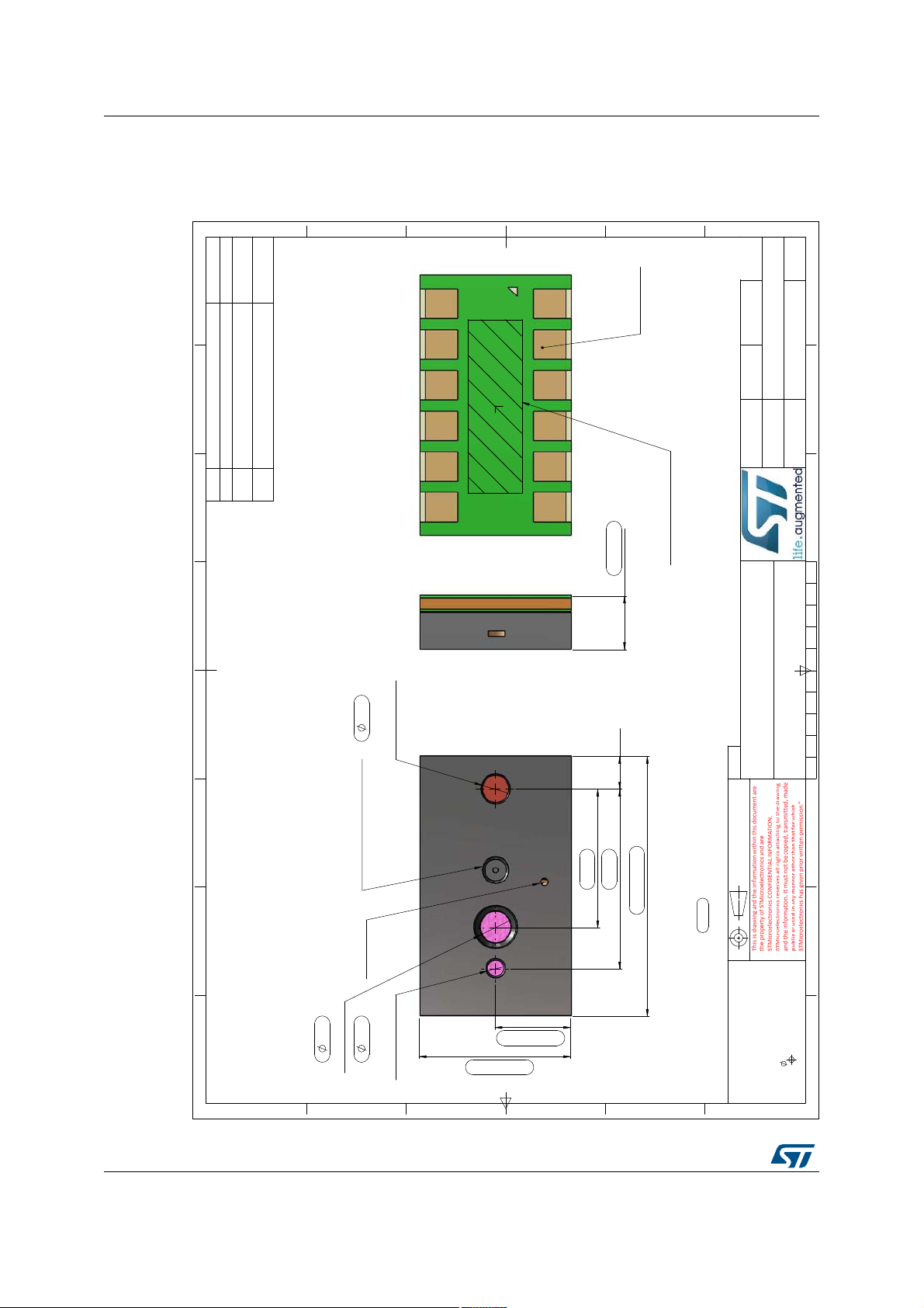
Outline drawing VL6180X
SEE SHEET 2
AREA RESERVED FOR
PART MARKING
8
Imaging Division
A
B
C
D
E
F
A
B
C
D
E
F
2
1
3
4
5
6
78
1
3
2
7
6
1 OF 2
DAVID MCARDLE
A
B
C
D
E
F
A
B
C
D
E
F
2
1
3
4
5
6
78
1
3
2
7
6
25:1
-
Do Not Scale
MODULE OUTLINE DRAWING
8432884
14 DEC 12
A
B
C
D
E
F
A
B
C
D
E
F
2
1
3
4
5
6
78
1
3
2
7
6
8
All dimensions
Part No.
in mm
Interpret drawing per BS8888,
Finish
8
Date
Material
Drawn
Tolerances, unless otherwise stated
8
Surface Finish 1.6 microns
A
B
C
D
E
F
A
B
C
D
E
F
2
1
3
4
5
6
78
1
3
2
7
6
8
A
B
C
D
E
F
A
B
C
D
E
F
Scale
2
1
3
4
5
6
78
1
3
2
7
6
VL6180 BABYBEAR CUT 1.0
0.10
3RD Angle Projection
A
B
C
D
E
F
A
B
C
D
E
F
Sheet
2
1
3
4
5
6
78
1
3
2
7
6
8
Title
Linear
0 Place Decimals 0 ±0.05
1 Place Decimals 0.0 ±0.05
2 Place Decimals 0.00 ±0.05
Angular ±0.25 degrees
Diameter
+0.05
Position
STMicroelectronics
-
VENT ONLY
3267,215(7851
$3(5785(
$/6$3(5785(
/,*+7(0,66,21
$3(5785(
GATE - COSMETIC
(SUPPLIER DEPENDENT)
5(9,6,216
5(9 '(6&5,37,21 ' $7(
% 83'$7('287/,1(725(029(*$7(,//8675$7,21
%
1(:'5$:,1*)5$0(216+7$7*5,' 5()'
',0(16,21'(/(7(',1/+9,(:*$7($''('
127(6
',0(16,2160$5.('7+86$5(72%(86('
$6,163(&7,21',0(16,216
VL6180X
7 Outline drawing
Figure 27. Outline drawing (page 1/2)
70/79 DocID026171 Rev 6
Page 71
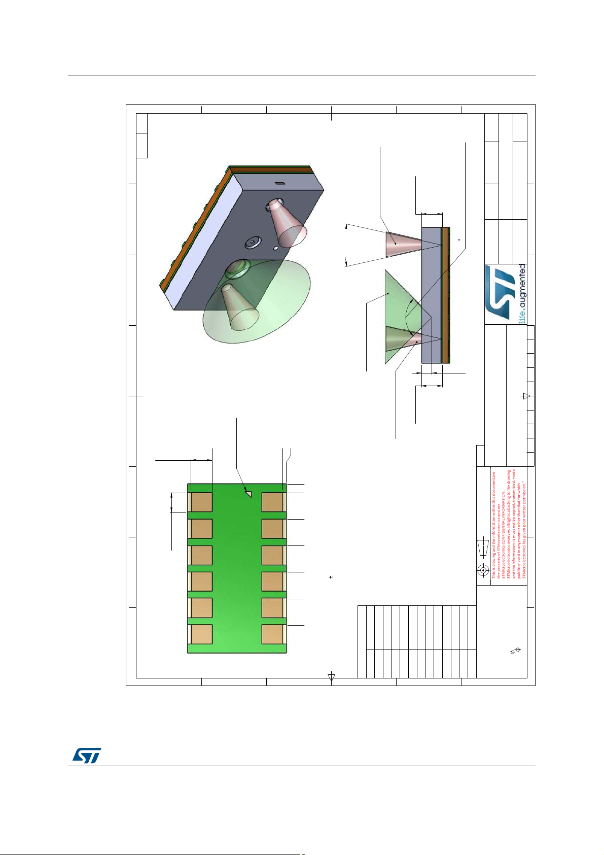
VL6180X Outline drawing
REV B1
&211(&7,217$%/(
3$'1R )81&7,21
*3,2
1&
1&
*3,2
6&/
6'$
1&
$9''B9&6(/
$966B9&6(/
$9''
1&
*1'
TOLERANCE 0.03 APPLIES
UNLESS OTHERWISE STATED
-
A
B
C
D
E
F
A
B
C
D
E
F
2
1
3
4
5
6
78
1
3
2
7
6
8
DAVID MCARDLE
A
B
C
D
E
F
A
B
C
D
E
F
2
1
3
4
5
6
78
1
3
2
7
6
2 OF 2
25:1
Imaging Division
MODULE OUTLINE DRAWING
8432884
14 DEC 12
A
B
C
D
E
F
A
B
C
D
E
F
2
1
3
4
5
6
78
1
3
2
7
6
8
VL6180 BABYBEAR CUT 1.0
8
All dimensions
Do Not Scale
in mm
Tolerances, unless otherwise stated
Interpret drawing per BS8888,
Part No.
Finish
Date
Drawn
Surface Finish 1.6 microns
A
B
C
D
E
F
A
B
C
D
E
F
2
1
3
4
5
6
78
1
3
2
7
6
8
A
B
C
D
E
F
A
B
C
D
E
F
Scale
2
1
3
4
5
6
78
1
3
2
7
6
8
0.10
3RD Angle Projection
A
B
C
D
E
F
A
B
C
D
E
F
Sheet
2
1
3
4
5
6
78
1
3
2
7
6
8
Title
Material
Linear
0 Place Decimals 0 ±0.05
1 Place Decimals 0.0 ±0.05
2 Place Decimals 0.00 ±0.05
Angular ±0.25 degrees
Diameter
+0.05
Position
STMicroelectronics
-
PIN INDICATOR
,1326
,1326
VIEW CONE
PROXIMITY SENSOR
ILLUMINATION CONE
PROXIMITY SENSOR
PROXIMITY SENSOR
ALS CONE
,1326
&21($3(;
)8//)29
$0%,(1775$160,66,21
&21($3(;
VL6180X
Figure 28. Outline drawing (page 2/2)
DocID026171 Rev 6 71/79
78
Page 72
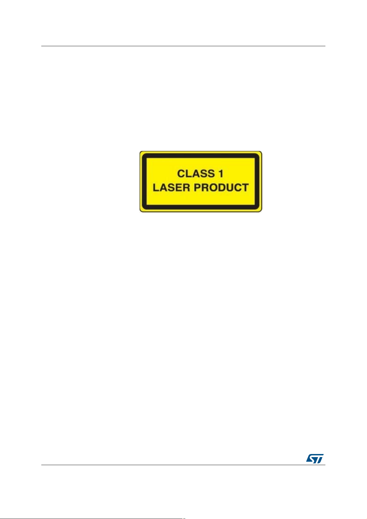
Laser safety considerations VL6180X
8 Laser safety considerations
The VL6180X contains a laser emitter and corresponding drive circuitry. The laser output is
designed to remain within Class 1 laser safety limits under all reasonably foreseeable
conditions including single faults in compliance with IEC 60825-1:2007. The laser output will
remain within Class 1 limits as long as the STMicroelectronics recommended device
settings are used and the operating conditions specified in this datasheet are respected.
The laser output power must not be increased by any means and no optics should be used
with the intention of focusing the laser beam.
Figure 29. Class 1 laser product label
8.1 Compliance
Complies with 21 CFR 1040.10 and 1040.11 except for deviati ons pur suan t to Laser Notice
No.50, dated June 24, 2007.
72/79 DocID026171 Rev 6
Page 73
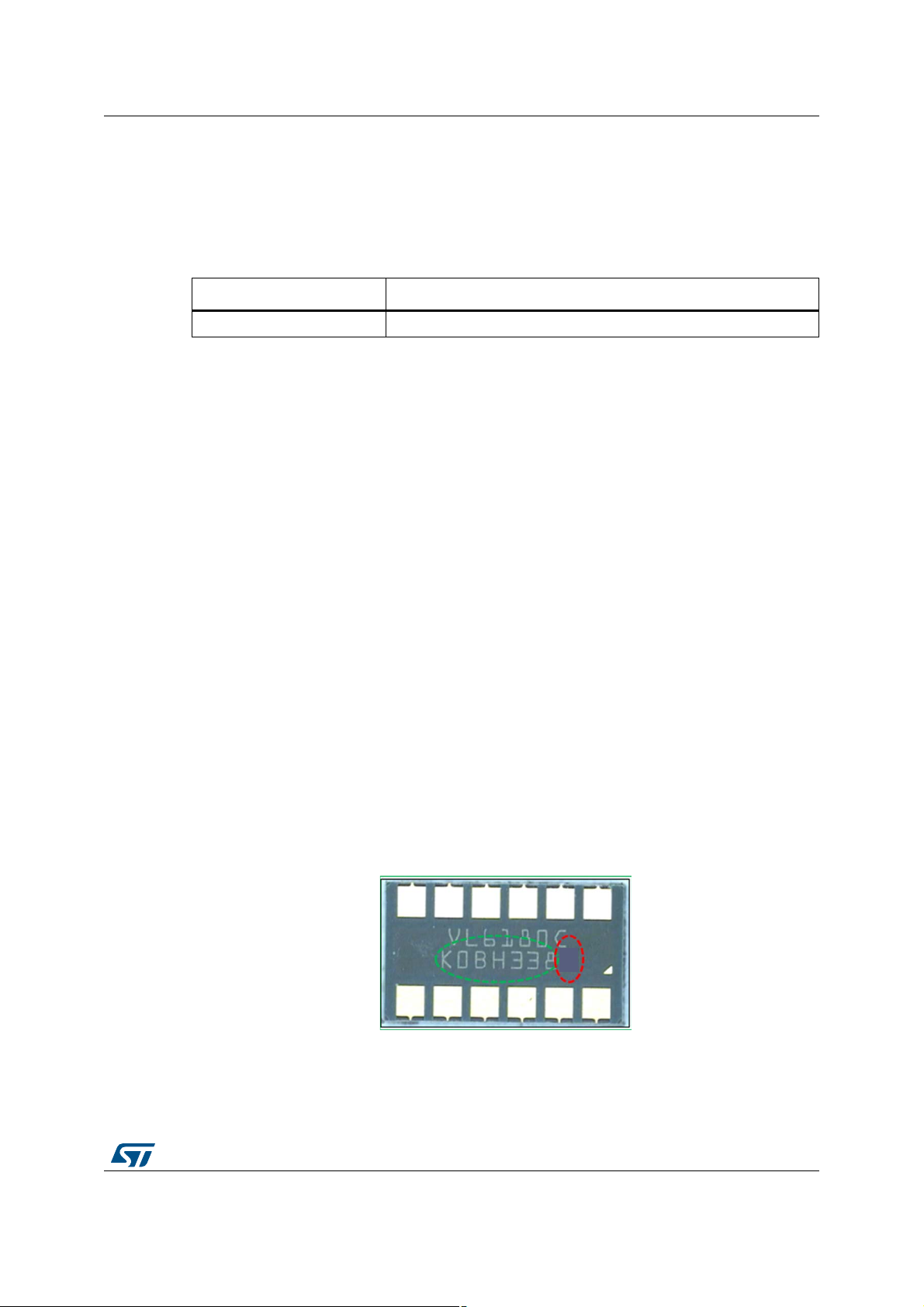
VL6180X Ordering information
D
9 Ordering information
VL6180X is currently available in the following format. More detailed informa tion is available
on request.
Order code Description
VL6180XV0NR/1 Tape and reel (5000 units in a reel)
9.1 Traceability and identification
Latest ROM revision can be identified as follows:
0x002 IDENTIFICATION__MODEL_REV_MINOR = 3
The minimum information required for traceability is the content of the following registers:
0x006 - IDENTIFICATION__DATE_HI
Table 26. Delivery format
0x007 - IDENTIFICATION__DATE_LO
0x008 - IDENTIFICATION__TIME (16-bit)
0x00A - IDENTIFICATION__CODE
With this information, the module can be uniquely identified.
Preferably, all the IDENTIFICATION register contents should be provided for traceability.
9.2 Part marking
Devices are marked on the underside as shown below. 1st line is the product ID. 2nd line is
the manufacturing info. (circled in green), where the 1st four letters are the lot ID and the
last 3 digits are the year + week number. Here: 338 is 2013 wk38. The final letter, circled in
red, is the ROM revision (‘D’).
Figure 30. Part marking
DocID026171 Rev 6 73/79
78
Page 74
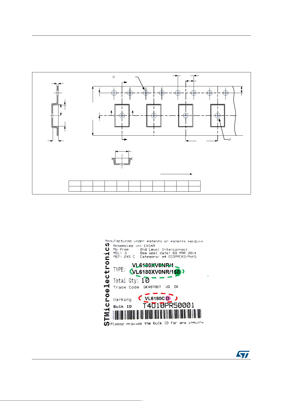
Ordering information VL6180X
0.30 0.05 (T)
+
-
5 °
5.10 (Bo)
1.20 (Ko)
12.0 0.3 (W)
+
-
5.5 0.05 (F)
+
-
B
B
SECTION B-B
SECTION A-A
3.10 (Ao)
A
A
1.55 0.1 (Do)
+
-
2.0 (P2)
4.0 (Po)
1.75 (E)
1.6 0.05 (D1)
+
-
8.0 (P1)
Ao 0.1
3.10
Bo 0.1
5.10
Ko 0.1
1.20
E 0.1
1.75
F 0.05
5.5
Po 0.1
4.0
P1 0.1
8.0
P2 0.1
2.0
Do 0.1
1.55
T 0.05
0.30
W 0.3
12.0
USER FEED
DIRECTION
+
-
+
-
+-+-+
-
+
-
+-+
-
+-+
-
+
-
9.3 Packaging
The Root part number 1 is available in tape and reel packaging as shown in Figure 31.
Figure 31. Tape and reel packaging
9.3.1 Package labeling
The labeling on the packing carton is shown in Figure 32. The latest ROM revision is
indicated alongside the order code (shaded green) and also after the product marking
(shaded pink).
Figure 32. Package labeling
74/79 DocID026171 Rev 6
Page 75
VL6180X Ordering information
9.4 Storage
The Root part number 1 is a MSL 3 package.
Table 27. Storage conditions
Level
31 Week
After this limit, dry bake to be done; 3 hours at 125
9.5 ROHS compliance
The Root part number 1 is Ecopack2 compliant as per ST definition.
Devices which are ROHS compliant even with use of ROHS exemption(s) and free of
Halogenated flame retardant are named ECOPACK2 devices with the following definition:
• ROHS complia nt ev en with us e of ROHS exe m pt ion (s )
• 500 ppm maximum of Antimony as oxide or organic compound in each organic assy
Materials (glue, substrate, mod compounds, housing...). Antimony in ceramic parts, in
glass and in solder alloy is not restricted.
• 900 ppm maximum Bromine + Chlorine in each organic ass materials (glue, substrate,
mold compounds, housing...)
These values are referring to maximum total content not to extractable ions content.
Purchasing specification of assembly materials can impose lower values for technical
reasons.
Floor Life (out of bag) at Factory
Ambient <30oC/60% RH
o
C.
ECOP ACK2 de vice s are of course fully compliant to ST banned and declarable substances
specification and for example cannot contain red Phosphorus flame retardant.
DocID026171 Rev 6 75/79
78
Page 76

ECOPACK
®
VL6180X
10 ECOPACK
In order to meet environmental requirements, ST offers these devices in different grades of
ECOPACK
specifications, grade definitions and product status are available at: www.st.com.
ECOPACK
®
packages, depending on their level of environmental compliance. ECOPACK®
®
is an ST trademark.
®
76/79 DocID026171 Rev 6
Page 77
VL6180X Revision history
11 Revision history
Table 28. Document revision history
Date Revision Changes
23-Sep-2013 1 Initial release.
General update for latest ROM revision:
Section 1.1: Technical specification updated
Section 1.4: Application schematic updated
Section 1.5: Recommended solder pad dimensions updated
Notes added to Figure 5.: Recommended reflow profile
Section 2.13: Ambient light sensor (ALS) updated.
30-Jan-2014 1.1
Section 3.1: Absolute maximum ratings added
Section 3.2: Normal operating conditions extended
Section 4: Performance specification added
Revised outline drawing added to Section 7: Outline drawing
Class 1 laser product label added to Section 7: Outline drawing
Section 9: Ordering information added information relating to
device marking and package labeling
Updates to the following sections:
Section 1.5: Recommended solder pad dimensions
Section 3.2: Normal operating conditions
Section 3.4: Electrical characteristics
02-Apr-2014 1.2
Section 4.1: Proximity ranging (0 to 100mm)
Added Section 4.2: ALS performance
Corrected error codes in.Section 6.2.38: RESULT__ALS_STATUS
Updated Section 6.2.20:
SYSRANGE__MAX_CONVERGENCE_TIME
Product code changed to VL6180X
09-Apr-14 2
Add documentation reference number (026171)
Update Disclaimer
ALS linearity spec updated in Section 4.2: ALS performance
Updated some detail in Table 1.: Technical specification
Added comment to Section 1.3: Device pinout stating that pins
15-May-14 3
labeled ‘no connect’ can optionally be connected to ground
Added test condition to Section 3.3: Current consumption
Errata corrections in 6.2.8, 6.2.35 and 6.2.54
Section 7: Outline drawing updated (no dimensional changes)
Dry bake conditions updated in Section 9.4: Storage
28-May-14 4 Added Section 8.1: Compliance
DocID026171 Rev 6 77/79
78
Page 78
Revision history VL6180X
Table 28. Document revision history (continued)
Date Revision Changes
Re-write of Section 2: Functional description.
Section 6: Device registers: Added introduction and minor
16-Jun-14 5
20-Aug-2014 6
corrections
Section 7: Outline drawing updated to Rev B1. Supplier dependent
gate mark added.
Updates:
Section 2.8.3: Signal-to-noise ratio (SNR): Clarified SNR
calculation.
Section 6: Device registers: Corrected a clarified some register
descriptions.
Typical ranging performance graph updated.
Delivery & manufacturing info updated.
78/79 DocID026171 Rev 6
Page 79

VL6180X
IMPORTANT NOTICE – PLEASE READ CAREFULLY
STMicroelectronics NV and its subsidiaries (“ST”) reserve the right to make changes, corrections, enhance ments, modifications, and
improvements to ST products and/or to this document at any time without notice. Purchasers should obtain the latest relevant information on
ST products before placing orders. ST products are sold pursuant to ST’s terms and conditions of sale in place at the time of order
acknowledgement.
Purchasers are solely responsible for the choice, selection, and use of ST products and ST assumes no liability for application assistance or
the design of Purchasers’ products.
No license, express or implied, to any intellectual property right is granted by ST herein.
Resale of ST products with provisions different from the information set forth herein shall void any warranty granted by ST for such product.
ST and the ST logo are trademarks of ST. All other product or service names are the property of their respective owners.
Information in this document supersedes and replaces information previously supplied in any prior versions of this document.
© 2014 STMicroelectronics – All rights reserved
DocID026171 Rev 6 79/79
79
 Loading...