

Page 1

FEATURES
• SMBus, version 1.0, Compliance
• Master mode function to interface with ACPI
compliant embedded controller
• Support Pentium and x86-based designs
• Supported by default embedded controller
firmware
• Accept up to 16 SCI inputs
• Programmable level or edge (falling and rising
edge) triggered SCI inputs
• 20 possible edge-sensitive programmable
General Purpose Inputs/Outputs per device
• Programmable addresses for cascading OZ992s
• 32KHz operating frequency
• Supports 3.3v or 5v supply
• LOW-power hardware-driven speaker alarm
output
• Software programming kit available
• SMBALERT# and SMIEVENT outputs
• 8 programmable interrupt inputs for SMI event or
SMBALERT#
• 8 Auto LED Flash(ALF) programmable outputs
with 10% or 50% duty cycles
ORDERING INFORMATION
OZ992S - 28 pin SSOP
OZ992
Intelligent Manager
Smart ACPI GPIO/SCI
GENERAL DESCRIPTION
Micro’s OZ992 Smart ACPI/SCI (System Control
O
2
Interrupt) General Purpose Input/Output unit allows
OEMs to transform their legacy systems to ACPI
compliant systems by supporting up to 16 extra SCI
inputs. Regular core logic chipsets, such as the Intel
430TX/BX and ACPI compliant embedded controllers
have limited allowance for the GPIO or SCI input
signals for the system. The OZ992 provides a bridge
between the chipsets and the rest of the system to
allow system designers a cost-effective way to
improvise for such a deficiency.
OZ992 provides up to 20 GPIO signals in regular
SMB slave mode. In addition, the OZ992 allows up to
16 System Control Interrupt (SCI) input transitions to
be written to the system’s embedded controller in
master mode. The OZ992 provides the perfect
solution for leading notebook vendors to stay ahead
of the competition.
The OZ992 is an SMBus 1.0 compliant ACPI GPIO
with 16 Programmable General Purpose I/Os pins
flexible for a variety of functions such as
programmable inputs/outputs, SMB/SMI interrupt
service, power-saving, modularized hardware ID, and
Auto LED Flash (ALF) status display. OZ992’s other
features include hardware-driven speaker alarm
output.
As a Pentium and x86-based system compatible
device, the OZ992 Smart ACPI GPIO is a highly costeffective and practical solution for today’s notebook
and palmtop computers, pen-based data systems,
personal digital assistants, and portable datacollection terminals.
7/13/00 OZ992-SF-1.7 Page 1
©Copyright 1998 by O2Micro All Rights Reserved
Page 2
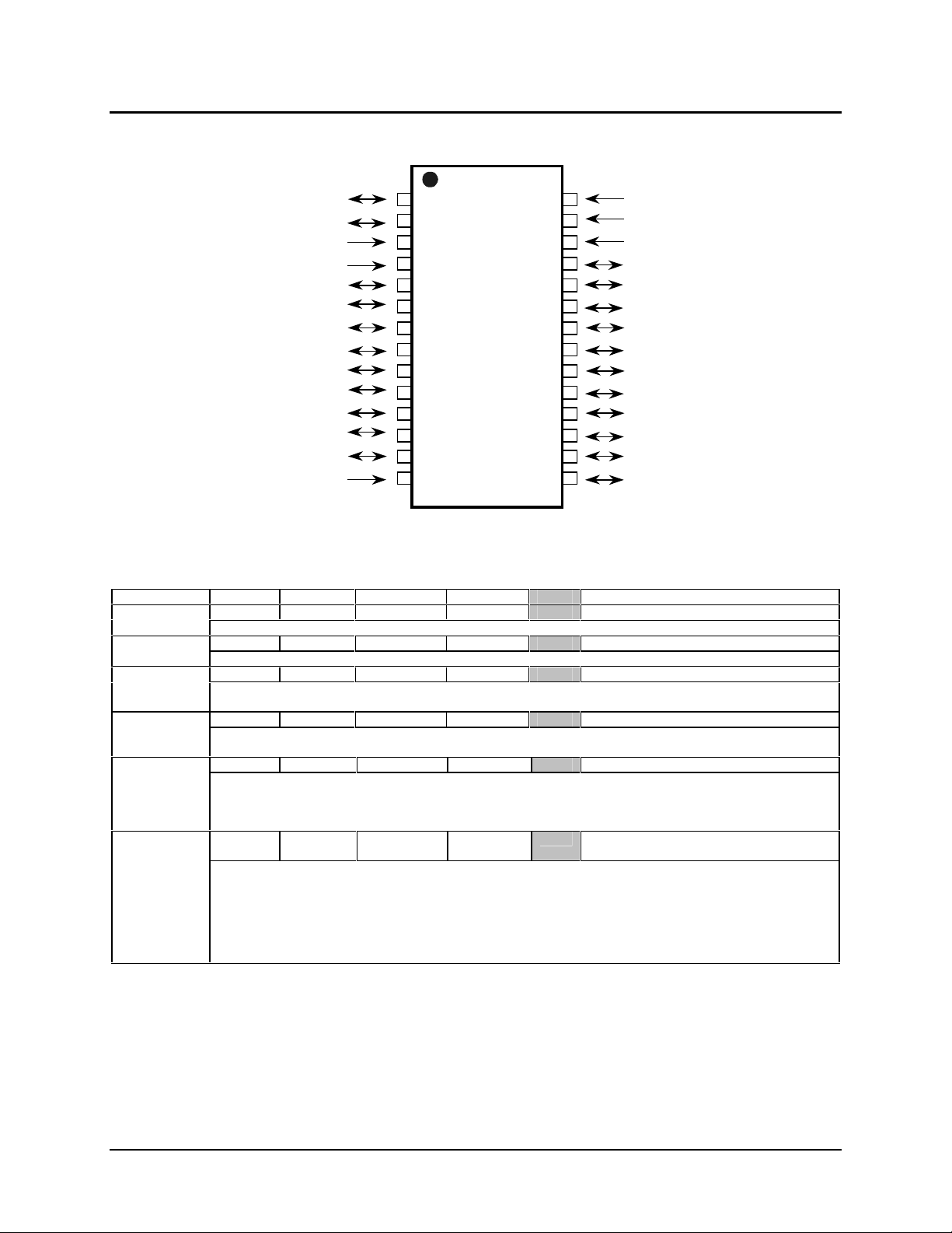
PIN DIAGRAM
OZ992
SMBCLK
SMBDATA
PWRGD
EOI#
GPIO[16]
GPIO[17]
GPIO[18]/TEST[0]
GPIO[19]/TEST[1]
GPIO[0]/SMIEVENT
GPIO[1]
GPIO[2]/SMBALERT#
GPIO[3]
GPIO[4]
GND
1
2
3
4
5
6
7
8
9
10
11
12
13
14
28
27
26
25
24
23
22
21
20
19
18
17
16
15
VCC
32KHZ
RESETN
GPIO[15]
GPIO[14]
GPIO[13]
GPIO[12]
GPIO[11]
GPIO[10]
GPIO[9]
GPIO[8]
GPIO[7]
GPIO[6]
GPIO[5]
PIN DESCRIPTION
Name Pin No. Type Input Drive Definition
SMBCLK
1 I TTL SMBus Clock Input for SMBus protocol communication.
SMBDATA
2 I/O TTL 12mA
SMBus Data Input/Output for SMBus protocol com munication.
PWRGD
3 I TTL -
This pin indicates that t he host system’s power, including the Core Logic chipsets , is stable. B efore the host
system’s power is stable, this input pin will tri-state all the output pins f rom OZ992.
EOI#
4 I TTL -
The embedded controller will signify the OZ992 when the activated SCI has been serviced. This pin is to be
used with EC master m ode onl y.
GPIO[17:16]
[6:5] I/O TTL 4mA
Fully programmable GPIOs that can be us ed for a variety of dedicated or s pecifi c func tions. Pins GP IO[17:16]
default as inputs. They are program m able t o func tion as eit her GPI [17:16] inputs or GPO[17:16] outputs . Refer
to GPIO[19:16] Config.1& 2 Registers for more detail s and GPIO Config. Tables (sec tion 5.0) for input/output
selections.
GPIO[19:18] /
[8:7] I/O TTL 4mA
TEST[1:0]
Fully programmable GPIOs that can be used for a variety of dedicated or specific functions. Pins
GPIO[19:18]/TEST[ 1:0] default as inputs . They are programmable to func tion as either GPI[19:18] inputs or
GPO[19:18] outputs. Refer to GPIO[19:16] Conf ig.1&2 Registers for more details and GPI O Config. Tables
(section 5.0) for input/ out put selections.
Ω
During regular usage, pull-ups of 47K
should be connec ted to GPIO[19:18] /TEST[1:0] to ensure the regular
OZ992 operation. Alternative uses f or GPIO[19:18] are as TES T[1:0], which provide 2 proprietary OZ992 test
modes.
SMBus Clock Input
SMBus Data Input/Output
Host System Power Good
End of Interrupt
General Purpose I/Os
General Purpose I/Os
OZ992-SF-1.7 Page 2
Page 3

Name Pin No. Type Input Drive
GPIO[0]/
SMIEVENT
GPIO[1]
GPIO[2]/
SMBALERT#
GPIO[7:3]
GPIO[15:8]
RESETN
32KHz
GND
VCC
9 I/O TTL 4mA
Fully programmable GPIOs that can be used for a variety of dedi cated or specifi c functions. Pin GPIO[0] has
SMIEVENT output as an alternate function. GPIO[0] defaults. It is also programmable to function as GPI[0]
input, GPO[0]output, A LF[0] output, or ID[0] input. Refer t o GPIO Config.1&2 Registers for more detail s and
GPIO Config. Tables (section 5.0) for input/output sel ections.
10 I/O TTL 4mA
Fully programmable GPIO that can be used for a variety of dedicated or specific functions. GPIO[1] pin defaults
as input. It is also programmable to func tion as GPI[1] input , GPO[1]output, ALF[1] output, or ID[1] input. Refer
to GPIO Config.1&2 Registers for more details and GPIO Config. Tables (section 5.0) for input/output
selections.
11 I/O TTL 4mA
Fully programmable GPIO that can be used for a variety of dedicated or specific functions. Pin GPIO[2] defaults
as input. This pin, when programmed as an alternate function, can generate the SMBALERT# interrupt.
SMBALERT# is an interrupt servi ce request signal t o the SMBus Host which c an be generated by all devices
connected to the OZ992. Pin GPI O[2]/SMBALERT# is also programm able to function as either GPI[2] input,
GPO[2] output, ALF[2] out put, or ID[2] input. Ref er to GPIO Config.1&2 Regist ers for more details and GPIO
Config. Tables (section 5.0) for I/O selections .
[17:15],
[13:12]
Fully programmable GPIOs that can be used f or a variety of dedicated or specific functions. GPIO[7:3] pi ns
default as inputs . They are program mabl e to funct ion as GPI [7:3] i nputs, GP O[7:3] out puts, A LF[7:3] out puts,
or ID[7:3] inputs. Refer t o GPIO Config.1&2 Regi sters for m ore details and GPIO Config. Tables (section 5.0)
for input/output selections.
[25:18] I/O TTL 4mA
Fully programmable GPIOs that can be us ed for a variety of dedic ated or specific functions. P ins GPIO[15:8]
default as inputs . P ins GP IO[ 15:8] as i nputs are program m able to generat e SMI/ SMB i nterrupts . They are al so
programmable to funct ion as GPI[15:8] inputs, GPO[15:8] output s. Refer to GPIO Config.1&2 Registers for
more details and GPIO Confi g. Tables (section 5.0) for i nput /output selections.
26 I TTL OZ992 hardware reset. RESETN(active LOW) resets all regis ters to t heir default values. This pin is connected
to the RC delay from the power supplied to OZ992.
27 I TTL 32KHz Clock Input.
14 GND - Ground.
28 PWR - -
3.3V or 5V Power Supply.
I/O TTL 4mA
GPIO Pins Alternate Usage
Definition
General Purpose I/O /
SMIEVENT
General Purpose I/O
General Purpose I/O /
SMBALERT#
General Purpose I/Os
General Purpose I/Os
Reset
32KHz Clock Input
Ground
3.3V/5V Power Supply
OZ992
19 16 15 8 7 0
GPIO[19:0]
SMIEVENT/SMBALERT#
SCI to Embedded Controller
OZ992-SF-1.7 Page 3
Page 4

DC CHARACTERISTICS
DC TABLE FOR VCC = 5.0V r 10%
Symbol Parameter Min Max Units
VCC
VIH
VIl
VOH
VOL
IIL
IOL
DC TABLE FOR VCC = 3.3V r 10%
Symbol Parameter Min Max Units
VCC
VIH
VIl
VOH
VOL
IIL
IOL
CAPACITANCE
Symbol Parameter
CIN
C
OUT
CIO
ABSOLUTE MAXIMUM RATINGS
Symbol Parameter Value Units
VCC
V
IN, VOUT
I
IN
T
STG
T
OPER|
ICC SPECIFICATIONS
Symbol Parameter Typ Max Units
ICC
Power Supply Voltage 4.5 5.5 V
Input HIGH Voltage 3.5 - V
Input LOW Voltage - 1.5 V
Output HIGH Voltage 2.4 - V
Output LOW Voltage - 0.4 V
Maximum Input Leakage Current -10 10
Maximum Output Leakage -10 10
Power Supply Voltage 3.0 3.6 V
Input HIGH Voltage 2.3 - V
Input LOW Voltage - 1 V
Output HIGH Voltage 2.4 - V
Output LOW Voltage - 0.4 V
Maximum Input Leakage Current -10 10
Maximum Output Leakage -10 10
0 qC to 70qC
Maximum Input Capacitance 10 pF
Maximum Output Capacitance 10 pF
Maximum I/O Capacitance 10 pF
DC Power Supply Voltage 3.0 to 3.6 V
DC Input, Output Voltage -0.3 to V
DC Current Drain V
Pins
Storage Temperature -40 to +125
Operation Temperature 0 to 70
Supply Current 50 60
and VSS
DD
+ 0.3 V
DD
±10
µA
µA
µA
µA
Units
mA
°C
°C
µA
OZ992
OZ992-SF-1.7 Page 4
Page 5
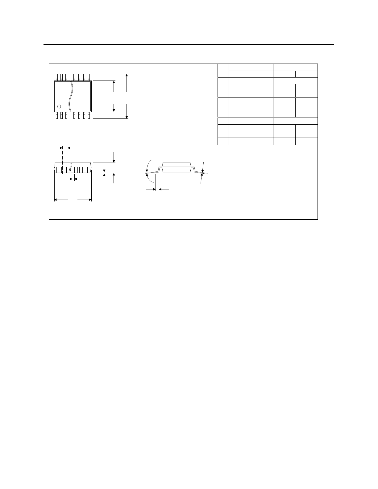
OZ992 PACKAGE INFORMATION
SSOP
E H
e
A
PACKAGE
(209 mil)
D
C
OZ992
DIM
A 0.084 2.13
A1 0.002 0.010 0.05 0.25
B 0.009 0.015 0.22 0.38
C 0.004 0.008 0.09 0.20
D 0.390 0.413 9.90 10.50
E 0.197 0.220 5.00 5.60
e 0.0256 0.65
H 0.291 0.323 7.40 8.20
L 0.025 0.041 0.63 1.03
α 0° 8° 0° 8°
INCHES MILLIMETERS
MIN MAX MIN MAX
D
B
A1
L
OZ992-SF-1.7 Page 5
 Loading...