

Page 1

FEATURES
• ACPI-PCI Bus Power Management Interface
Specification Rev 1.1 Compliant
• Supports OnNow LAN wakeup, OnNow Ring Indicate,
PCI CLKRUN#, PME#, and CardBus CCLKRUN#
• Compliant with PCI specification v2.2, 2000 PC Card
Standard 7.1
• Yenta™ PCI to PCMCIA CardBus Bridge register
compatible
• ExCA (Exchangeable Card Architecture) compatible
registers mappable in memory and I/O space
• Intel
• Supports PCMCIA_ATA Specification
• Supports 5V/3.3V PC Cards and 3.3V CardBus cards
• Supports two PC Card or CardBus slots with hot
• Supports multiple FIFOs for PCI/CardBus data transfer
• Supports Direct Memory Access for PC/PCI and
• Programmable interrupt protocol: PCI, PCI+ISA,
• Win’98 IRQ and PC-98/99 compliant
• Supports parallel or serial interface for socket power
• Zoomed Video Support; Zoomed Video Buffer Enable
• D3
• 3.3Vaux Power Support
• Integrated PC 98/99 -Subsystem Vendor ID support,
• LED Activity Pins
ORDERING INFORMATION
OZ6933T – 208 pin TQFP
OZ6933B – 208 pin Mini-BGA
GENERAL DESCRIPTION
The OZ6933 is an ACPI and PC98/99 logo certified, high
performance, dual slot PC Card controller with a synchronous 32-bit bus master/target PCI interface. This PC Card
to PCI bridge host controller is compliant with the 2000 PC
Card Standard. This standard incorporates the new 32-bit
TM
82365SL PCIC Register Compatible
insertion and removal
PCI/Way on PC Card socket
PCI/Way, or PC/PCI interrupt signaling modes
control including devices from Micrel and TI
Pins
state PME# wakeup support
cold
with auto lock bit
OZ6933
ACPI CardBus Controller
CardBus while retaining the 16-bit PC Card specification as
defined by PCMCIA release 2.1. CardBus is intended to
support “temporal” add-in functions on PC Cards, such as
Memory cards, Network interfaces, FAX/Modems and other
wireless communication cards, etc. The high performance
and capability of the CardBus interface will enable the new
development of many new functions and applications.
The OZ6933 CardBus controller is compliant with the latest
ACPI-PCI Bus Power Management Interface Specification.
It supports all four power states and the PME# function for
maximum power savings and ACPI compliance. Additional
compliance to OnNow Power Management includes D3
state support, paving the way for low sleep state power
consumption and minimized resume times. To allow host
software to reduce power consumption further, the OZ6933
provides a power-down mode in which internal clock
distribution and the PC Card socket clocks are stopped. An
advanced CMOS process is also used to minimize system
power consumption.
The OZ6933 dual PCMCIA socket supports two 3.3V/5V
8/16-bit PC Card R2 cards or 32-bit CardBus R3 cards. The
R2 card support is compatible with the Intel 82365SL PCIC
controller, and the R3 card support is fully compliant with
the 2000 PC Card Standard CardBus specification. The
OZ6933 is a stand alone device, which means that it does
not require an additional buffer chip for the PC Card socket
interface. In addition, the OZ6933 supports dynamic PC
Card hot insertion and removal, with auto configuration
capabilities.
The OZ6933 is fully compliant with the 33Mhz PCI Bus
specification, v2.2. It supports a master device with internal CardBus direct data transfer. The OZ6933 implements a
FIFO data buffer architecture between the PCI bus and
CardBus socket interface to enhance data transfers to
CardBus devices. The bi-directional FIFO buffer permits the
OZ6933 to accept data from a target bus (PCI or CardBus
interface) while simultaneously transferring data. This
architecture not only speeds up data transfers but also
prevents system deadlocks.
The OZ6933 is a PCMCIA R2/CardBus controller, providing
the most advanced design flexibility for PC Cards that interface with advanced notebook designs.
cold
07/20/00 OZ6933-SF-1.7 Page 1
Copyright 2000 by O2Micro All Rights Reserved
Page 2
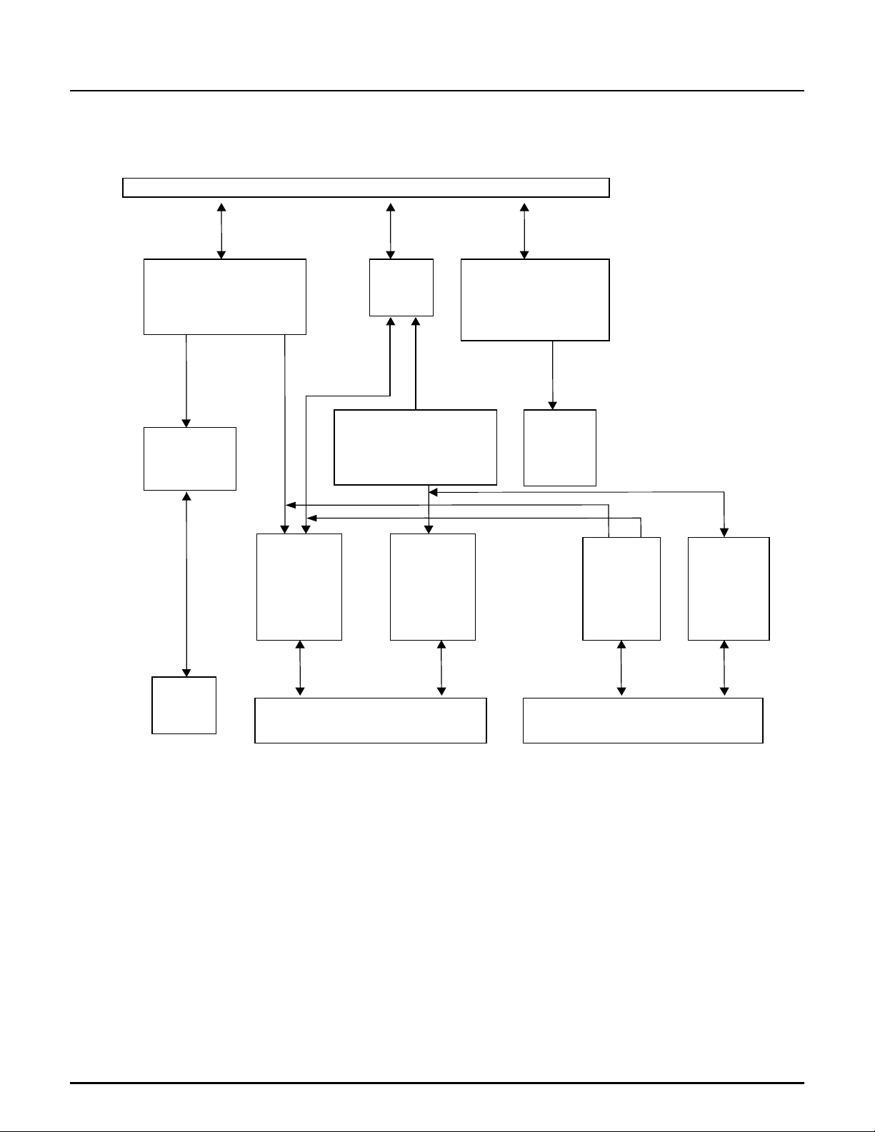
FUNCTIONAL BLOCK DIAGRAM
PCI Interface
OZ6933
PCI Configuration/
Function Control Registers
Power Switch
Control
PCI
Function Control
Configuration/
Registers
Power
Contro
Switch
l
PC Card
Machine
EXCA
8/16-Bit
16-
PC
Bit
Machin
Card
State
e
PCI
PCI
Arbite
Arbiter
r
CardBus FIFO
CardBu
Data Buffering
s
CardBus
PC Card
State
Machine
and
Arbiter
FIFO
ACPI/ OnNow
Power Management
for PC99
Interrupt
Subsystem
Interrup
t
EXCA
8/16 Bit
PC Card
State
Machine
CardBus
PC Card
State
Machine
and
Arbiter
Powe
Power
Switc
r
Switch
h
Interface
Socket A PC Card Interface
PC Card
Interface
Socket B PC Card Interface
OZ6933-SF-1.7 Page 2
Page 3
OZ6933
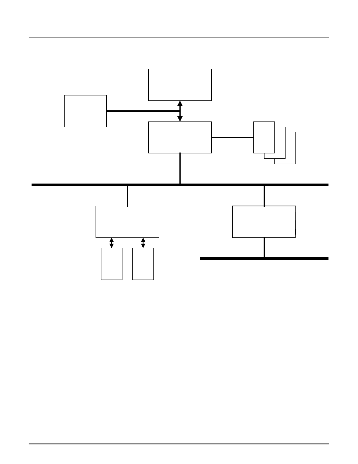
SYSTEM BLOCK DIAGRAM
The following diagram is a typical system block diagram utilizing the OZ6933 ACPI CardBus controller with other related
chipsets.
CPU
PCI Bus
VGA
AGP
OZ6933
CardBus
Controller
PC
Card
PC
Card
Memory
North Bridge
South Bridge
ISA
OZ6933-SF-1.7 Page 3
Page 4
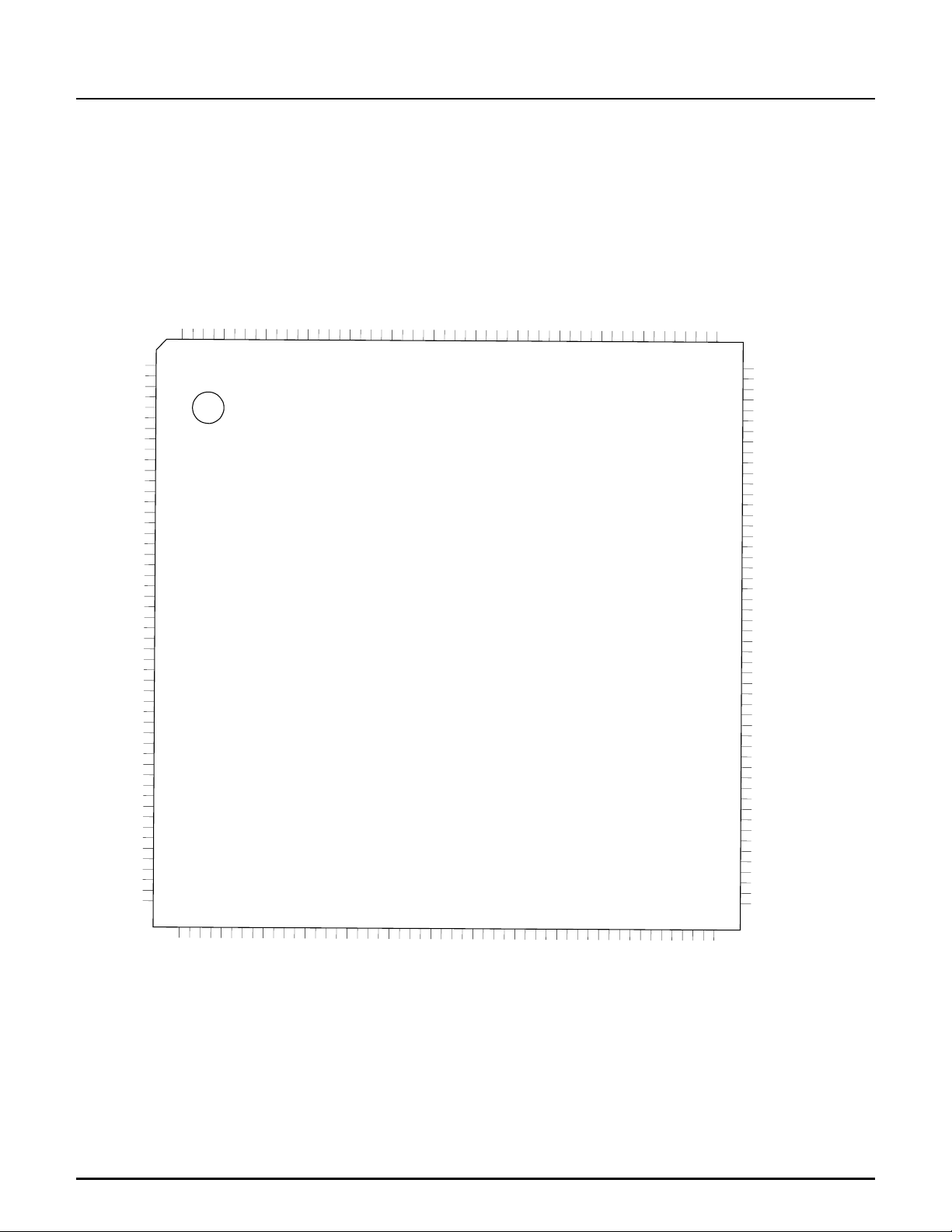
PIN DIAGRAM - 208 PIN TQFP
OZ6933
IRQ7/SIN#/B_VPP_PGM
B_RESET/CRESET#
B_WP/CCLKRUN#
IRQ14/CLKRUN#
IRQ5/SERIRQ
RST#
2
2
2
2
0
0
0
P
C
I
C
K
_
L
P
C
N
G
#
I
T
_
P
E
C
Q
R
I
_
#
1
3
A
D
0
3
A
D
P
C
C
V
I
C
_
A
D
9
2
A
D
8
2
A
D
7
2
A
D
6
2
5
2
A
D
4
2
A
D
C
/
#
B
E
3
C
R
G
O
E
_
N
D
I
D
S
E
L
A
D
3
2
A
D
2
2
A
D
1
2
A
D
0
2
A
D
9
1
P
C
V
I
C
_
C
A
8
1
D
7
1
A
D
1
A
D
6
C
/
#
B
E
2
C
R
O
E
_
D
N
G
R
F
A
M
E
#
C
N
R
G
O
E
_
D
I
R
D
Y
#
Y
T
R
D
#
E
D
V
#
S
E
L
S
P
#
T
O
P
E
R
R
#
S
E
R
R
#
P
A
R
C
/
B
#
E
1
P
C
V
I
C
_
C
A
D
5
1
A
D
1
4
A
D
3
1
2
1
A
D
1
1
A
D
1
A
D
0
C
R
G
O
E
_
N
D
A
D
9
A
D
8
C
/
B
#
E
0
A
D
7
6
A
D
P
C
V
I
C
_
C
A
D
5
4
A
D
0
1
2
3
4
5
6
7
8
9
1
1
1
1
1
1
1
1
1
1
2
2
2
2
2
2
2
2
2
2
3
3
3
3
3
3
3
3
3
9
3
0
4
1
4
2
4
3
4
4
4
5
4
6
4
7
4
4
8
9
4
0
5
1
5
2
5
5
6
7
8
0
1
2
3
4
5
6
7
8
9
0
1
2
3
4
5
6
7
8
9
0
1
2
3
4
5
6
7
8
5
5
5
5
3
4
6
5
B_SOCKET_VCC
B_CD2#/CCD2#
IRQ4/INTB#
2
0
4
5
7
B_D10/CAD31
B_D2/RFU
INTA#
2
0
3
5
5
8
9
1
1
2
2
2
0
0
0
9
9
0
1
2
8
9
6
6
6
6
3
2
1
0
IRQ11/SKTB_ACTV
B_BVD1/CSTCHG
B_D0/CAD27
B_D8/CAD28
B_D1/CAD29
B_D9/CAD30
1
1
9
9
7
6
6
6
4
5
B_A0/CAD26
1
1
1
1
1
9
9
9
9
9
2
3
4
5
1
6
6
6
7
6
6
9
8
7
0
B_INPACK#/CREQ#
B_WAIT#/CSERR#
B_REG#/CC_BE3#
B_BVD2/CAUDIO
B_A2/CAD224
B_A3/CAD23
B_A1/CAD25
1
1
1
1
1
1
8
8
7
4
8
8
7
6
O2M
7
7
6
5
8
5
O
1
8
4
i
Z
7
7
8
7
9
8
0
9
7
7
7
1
2
3
B_VS2/CVS2
B_A6/CAD20
B_A5/CAD21
B_A4/CAD22
CORE_VCC
GND
1
1
1
1
1
1
8
8
2
3
c
r
o
6
9
8
7
9
0
1
8
8
7
7
7
0
1
9
8
7
,
I
n
c
.
3
3
8
8
8
8
4
1
3
2
B_A23/CFRAME#
B_A12/CCBE2#
B_A24/CAD17
B_A25/CAD19
B_A7/CAD18
1
1
1
1
1
7
7
7
7
7
4
2
5
6
3
8
8
8
8
8
6
5
9
8
7
B_RDY_IREQ#/CINT#
B_A21/CDEVSEL#
B_A20/CSTOP#
B_A22/CTRDY#
B_A15/CIRDY#
1
1
7
7
0
1
9
9
9
1
0
2
B_WE#/CGNT#
B_A16/CCLK
1
1
1
1
1
6
6
6
6
6
9
8
7
5
6
9
9
9
9
3
4
5
6
B_SOCKET_VCC
B_A19/CBLOCK#
B_A14/CPERR#
IRQ12/PME#
1
1
1
6
6
6
2
3
4
9
9
9
9
8
7
B_A8/CCBE1#
B_A17/CAD16
B_A13/CPAR
B_A18/RFU
1
1
1
1
1
6
5
5
6
5
5
1
6
I
W
B
O
_
/
C
#
A
R
D
5
1
8
9
0
7
5
5
1
5
1
5
1
1
5
5
1
5
1
4
1
1
4
4
1
4
1
4
1
4
1
4
1
4
1
4
1
4
1
3
1
3
1
1
3
3
1
3
1
3
1
3
1
3
1
3
1
3
1
2
1
2
1
2
1
1
2
2
1
2
1
2
1
1
2
2
1
2
1
1
1
1
1
1
1
1
1
1
1
1
1
1
1
1
1
1
1
1
1
0
1
0
1
1
0
0
1
1
1
1
1
1
0
1
0
0
0
0
0
3
2
1
0
4
A
B
_
4
B
I
O
_
3
A
B
_
2
V
B
_
1
O
B
_
0
B
C
_
9
A
B
_
8
D
B
_
7
B
_
C
6
V
B
_
5
D
B
_
4
D
B
_
3
B
S
_
2
D
B
_
1
D
B
_
0
D
B
_
9
B
D
_
8
D
B
_
7
D
B
_
6
B
_
C
5
B
D
_
4
R
O
C
3
E
D
L
2
S
C
L
1
S
D
A
0
A
S
L
9
C
R
O
8
S
P
K
7
X
A
U
6
C
A
_
5
W
A
_
4
A
D
_
3
D
A
_
2
D
A
_
1
A
_
D
0
A
D
_
9
D
A
_
8
B
V
A
_
7
_
G
R
6
A
0
A
_
5
V
P
A
_
4
B
A
_
3
2
1
0
9
8
7
6
5
V
A
A
1
_
R
A
_
A
A
2
_
I
A
_
N
A
A
3
_
W
A
_
A
4
A
_
A
_
R
E
A
5
A
_
1
/
4
9
C
1
A
D
R
D
/
C
#
A
D
3
1
/
C
1
1
A
D
2
1
S
/
1
C
V
S
1
/
E
#
C
A
D
1
1
/
C
#
E
2
A
D
0
1
/
0
1
C
A
D
9
1
A
D
/
C
5
8
/
C
#
E
1
C
#
B
E
0
V
P
P
_
C
C
4
1
U
F
/
R
A
D
/
C
7
7
K
E
C
O
V
C
_
T
C
/
C
3
1
A
D
6
/
6
A
D
C
5
/
C
2
A
1
D
4
/
C
5
A
D
3
/
C
1
1
A
D
2
4
/
C
A
D
1
/
D
#
C
C
1
D
#
1
A
/
C
3
D
0
E
_
C
V
C
U
/
O
T
S
_
K
A
C
_
T
I
T
V
I
Y
K
/
V
C
A
_
A
T
/
B
V
_
C
T
H
/
B
_
N
G
D
E
_
U
O
_
R
T
V
C
_
C
D
/
#
C
C
2
P
/
C
C
K
L
A
/
C
0
1
D
/
R
2
U
F
9
A
D
/
C
3
A
D
/
C
2
1
/
C
8
A
D
2
/
C
0
A
D
2
D
/
S
1
T
S
S
#
T
/
C
A
D
6
2
P
V
C
_
C
A
D
/
C
2
/
C
A
D
5
2
#
E
G
/
C
C
/
4
C
2
A
D
K
#
P
A
C
/
C
A
D
3
2
A
I
T
/
C
#
S
/
C
A
D
2
2
S
E
/
T
C
/
C
A
1
2
D
T
C
#
5
#
3
C
C
V
C
#
5
C
_
#
D
2
#
R
#
U
N
1
3
0
9
8
7
C
H
G
U
D
I
O
B
E
3
#
R
/
#
E
C
Q
E
R
R
#
E
S
E
#
T
R
AD0
AD3
AD2
AD1
CORE_GND
LOCK#
A_D3/CAD0
A_SOCKET_VCC
A_CD1#/CCD1#
A_D4/CAD1
A_D11/CAD2
A_D5/CAD3
A_D12/CAD4
A_D6/CAD5
A_D13/CAD6
A_D7/CAD7
A_D14/RFU
A_CE1#/CCBE0#
A_D15/CAD8
IRQ15/RING_OUT
A_A10/CAD9
A_CE2#/CAD10
A_OE#/CAD11
A_VS1/CVS1
A_A11/CAD12
A_IORD#/CAD13
CORE_VCC
A_A9/CAD14
A_IOWR/CAD15
A_A8/CCBE1#
A_A17/CAD16
A_A13/CPAR
A_A18/RFU
A_A14/CPERR#
IRQ3/VCC3#
A_A19/CBLOCK#
A_WE#/CGNT#
A_A20/CSTOP#
A_RDY_IREQ#/CINT#
A_A21/CDEVSEL#
A_A16/CCLK
A_A22/CTRDY#
A_A15/CIRDY#
A_A23/CFRAME#
A_A12/CCBE2#
SOCKET_VCC
A_A24/CAD17
A_A7/CAD18
GND
A_A25/CAD19
A_A6/CAD20
A_VS2/CVS2
OZ6933-SF-1.7 Page 4
Page 5
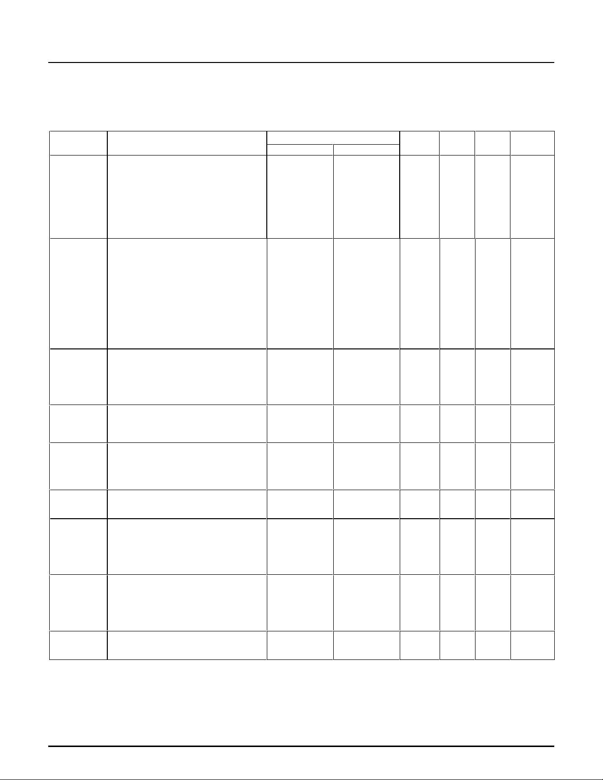
PIN LIST
Bold Text = Normal Default Pin Name
PCI Bus Interface Pins
Pin Name Description
AD[31:0]
C/BE[3:0]#
FRAME#
IRDY#
TRDY#
STOP#
IDSEL
DEVSEL#
PERR#
PCI Bus Address Input/Data: These
pins connect to PCI bus signals AD[31:0].
A Bus transaction c onsists of an address
phase followed by one or more data
phases.
PCI Bus Command/Byte Enable: The
command signali ng and byte enables are
multiplexed on the same pins . During the
address phase of a transaction,
C/BE[3:0]# are interpreted as the bus
commands. During the data phase,
C/BE[3:0]# are interpreted as byte
enables. The byte enables are to be val id
for the entirety of each data phase, and
they indicate which bytes in t he 32-bit data
path are to carry meaningful dat a for the
current data phase.
Cycle Frame: This input indicates to the
OZ6933 that a bus transaction is
beginning. While FRAME# is asserted,
data transfers continue. When FRAME#
is de-asserted, the transaction is in its final
phases.
Initiator Ready: This input indicates the
initiating agent’s ability to complete the
current data phase of the transaction.
IRDY# is used in conjunction with TRDY#.
Target Ready: This output indicates
target Agent’s the OZ6933’s ability to
complete the current data phase of the
transaction. TRDY# is used in conjunction
with IRDY#.
Stop: This output indicates the current
target is requesting the m aster to s top the
current transaction.
Initialization Device Select: This input is
used as chip select during configuration
read and write transactions. This is a
point-to-point signal. IDS EL can be used
as a chip selec t during configuration read
and write transactions.
Device Select: This output is driven
active LOW when the PCI address is
recognized as supported, thereby acting
as the target for the current PCI cycle.
The Target must respond before timeout
occurs or the cycle will terminate.
Parity Error: The output is driven active
LOW when a dat a parity error is detected
during a write phase.
OZ6933
Pin Number
TQFP BGA
4-5, 7-12, 1620, 22-24, 3843, 45-46, 48-
49, 51-56
13, 25, 36, 47 G1, K3, M3, R1 TTL I/O 4 -
27 K6 TTL I/O 4
29 L1 TTL I/O 4 -
30 L2 TTL I/O 4 PCI Spec
32 L5 TTL I/O 4 PCI Spec
15 H5 TTL I 4 -
31 L3 TTL I/O 4 PCI Spec
33 L6 - TO 4 PCI Spec
E1, E2, F3, F1,
G5, H6, G3,
G2, H2, H1, J1,
J2, J3, J6, K1,
K2, M5, N2,
N1, N3, N6, P1,
P3, N5, P6, R2,
R3, T1, W4,
R6, U5, P7
Input Type
TTL I/O 4 PCI Spec
Power
Rail
Drive
-
OZ6933-SF-1.7 Page 5
Page 6
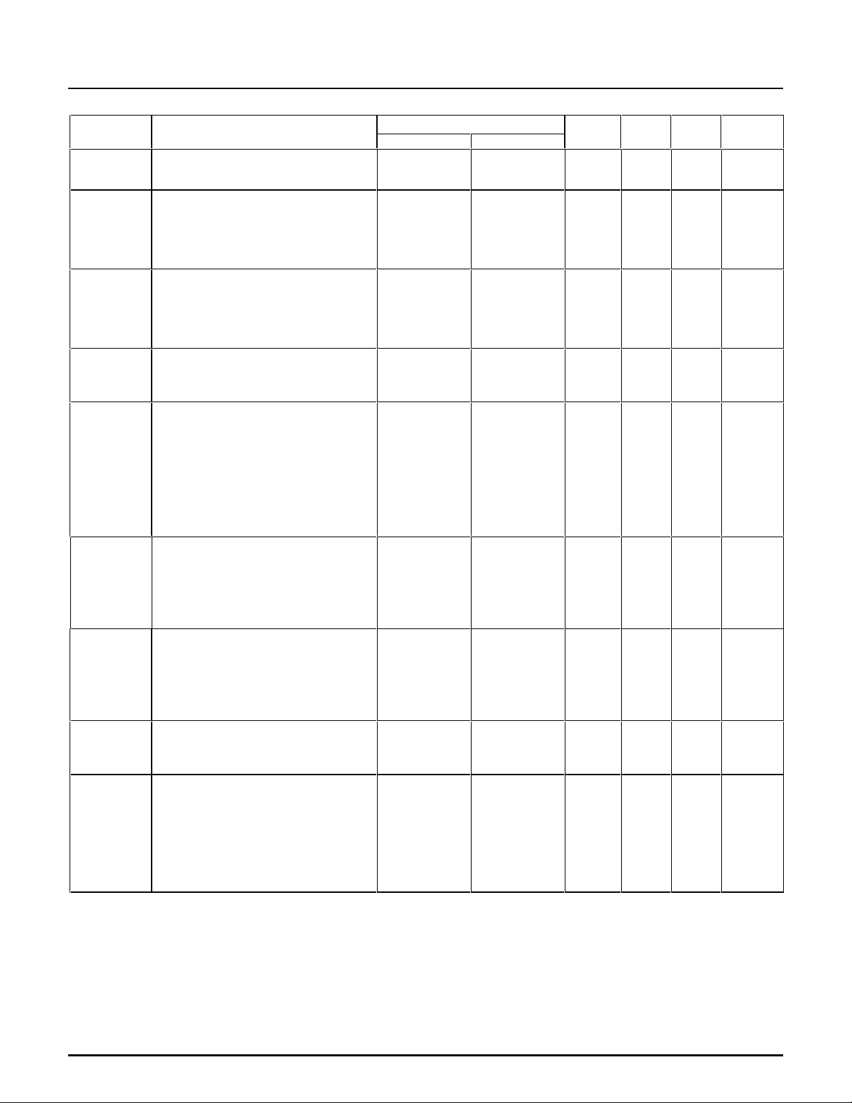
Pin Name Description
SERR#
PAR
PCI_CLK
RST#
RI_OUT
CLKRUN#
PME#
SKTB_ACTV
INTA#
System Error: This output is driven
active LOW t o indicate an address parity
error.
Parity: This pin generates PCI parity and
ensures even parity across A D[31:0] and
C/BE[3:0]#. During the address phase,
PAR is valid after one clock. W ith data
phases, PAR is stable one clock after a
write or read transaction.
PCI Clock: This input provides timing for
all transactions on the PCI bus to and from
the OZ6933. All PCI bus signal s, except
RST#, are sampled and driven on the
rising edge of PCI_CLK. This input can be
operated at frequencies from 0 to 33MHz.
Device Reset: This input is used to
initialize all registers and internal logic to
their reset states and plac e most OZ6933
pins in a HIGH-impedance s t ate.
Ring Indicate Out: This pin is Ring
Indicate when the following occurs while
Mode Control B Register (index 2Eh)
O
2
bit 7 is set to 1:
1) Power Control (Index+02h) bit 7 set
to 1
2) Interrupt and General Control
(Index+03h) bit 7 set to 1
3) PCI O
PCI Clock Run Request: This signal is
used by the central resource to request
permission to stop the PCI clock or to slow
it down, and the OZ6933 responds
accordingly. To enable the CLKRUN#
signal, you need to enable ExCA register
3B bit[3:2].
Power Management Event: A power
management event is the process by
which the OZ6933 can request a change
of its power consumption state. Usual l y, a
PME occurs during a request to change
from a power saving state to the fully
operational state.
Socket B Activity: This signal indicates
that there is any activit y on the socket B
read/write access. Refer to PCI
Configuration Register 90h.
PCI Bus Interrupt A: This output
indicates a programmable interrupt
request generated from any of a number
of card actions. Although there is no
specific mapping requirement for
connecting interrupt lines from the
OZ6933 to the system , a common use is
to connect this pin to t he system PCI bus
INTA# signal.
Micro Control 2 (Offset: D4h)
2
bit X = 0
OZ6933
Pin Number
TQFP BGA
34 M1 - TO 4 PCI Spec
35 M2 TTL I/O 4 PCI Spec
1 E3 TTL I 4 -
207 D1 TTL I 1 -
72 V9 - TO 1 6mA
208 A4 TTL I/O 4 PCI Spec
163 B14 - TO 1 6mA
193 E8 - TO 1 6mA
203 B5 - TO 4 PCI Spec
Input Type
Power
Rail
Drive
OZ6933-SF-1.7 Page 6
Page 7
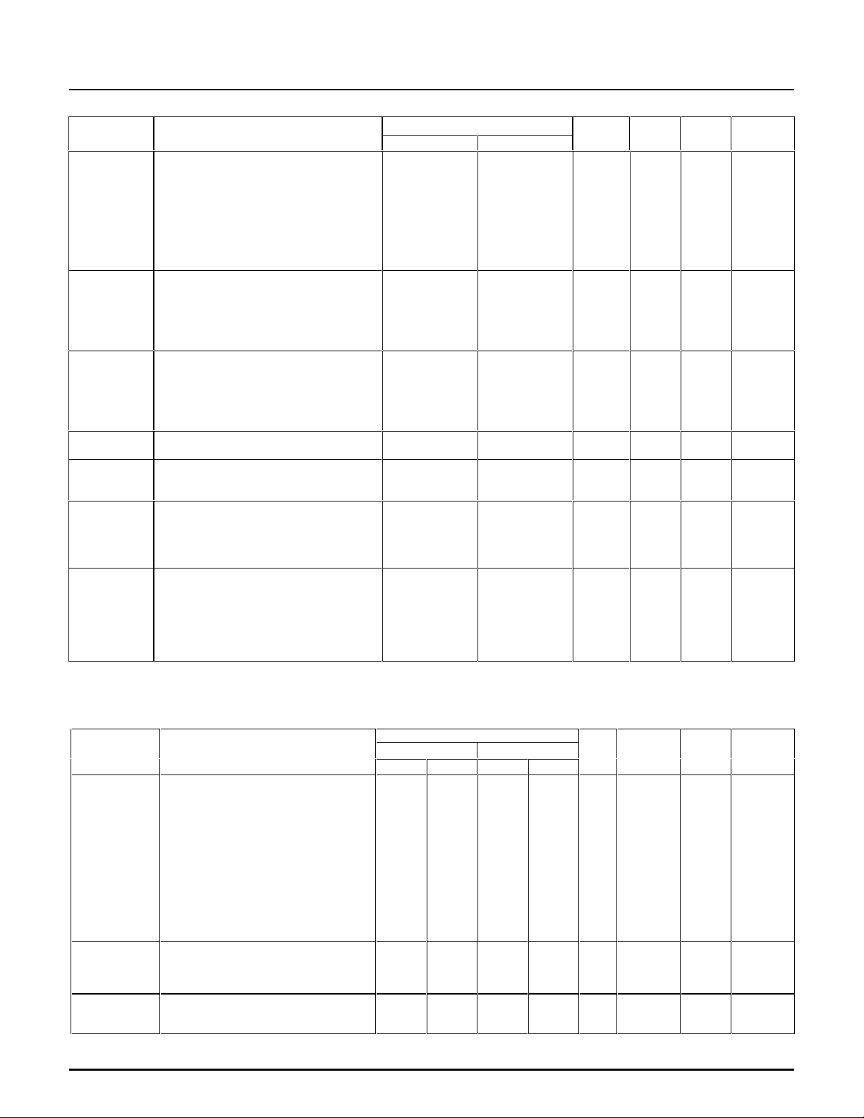
Pin Name Description
INTB#
IRQSER/
SOUT#/
IRQ5
IRQ7/SIN#/
B_VPP_PGM
GNT#
REQ#
LOCK#
PCI_VCC
PCI Bus Interrupt B: This output
indicates a programmable interrupt
request generated from any of a number
of card actions. Although there is no
specific mapping requirement for
connecting interrupt lines from the
OZ6933 to the system , a common use is
to connect this pin to t he system PCI bus
INTB# signal.
IRQSER/SOUT#/IRQ5: In PC/PCI Serial
Interrupt Signaling mode, this pin is the
serial interrupt output, SOUT#. In PC/Way
mode, this pin is t he IRQ serializer pin to
the interrupt controller. I n the parallel ISA
mode, this pin is t he ISA IRQ5
IRQ7/SIN#/B_VPP_PGM: In PC/PCI
Serial Input Si gnaling m ode, this pin is the
serial interrupt input, S IN#. In the parallel
ISA mode, thi s pin is the ISA IRQ7. This
pin also can be configured as parallel
power control pin B_VPP_PGM
Grant: This signal indicates that access
to the bus has been granted.
Request: This signal indicates to the
arbiter that the OZ6933 requests use of
the bus.
PCI LOCK#: This signal is used by a PCI
master to perf orm a locked transact ion to
a target memory. LOCK# is used to
prevent more than one mast er from using
a particular system resource.
PCI Bus VCC: These pins must be
connected to a 3.3-volt power supply. The
PCI bus interface pin output s listed in this
table (Table 2-1) will operate at the
voltage applied to these pins , i ndependent
of the voltage appl ied to ot her OZ6933 pin
groups.
PCMCIA Sockets Interface Pins
Socket A pin number --- Socket B pin number
Name1 Description2
-REG#/
CCBE3#
A[25:24]/
CAD[19, 17]
A23/
CFRAME#
Register Access: During PCMCIA
memory cycles, this output chooses
between attribute and common
memory. During I/O cycles for non-DMA
transfers, this signal is active (low).
During ATA mode, t his signal is al ways
inactive. For DMA cycles on the
OZ6933 to a DMA-capable card, -REG
is inactive during I/O c ycles to indicate
DACK to the PCMCIA card.
CardBus Command Byte Enable: In
CardBus mode, this pi n i s the CCBE3#.
PCMCIA socket address 25:24 outputs.
CardBus Address/Data: CardBus
mode, these pins are the CA D bits 19
and 17.
PCMCIA socket address 23 output.
CardBus Frame: In CardBus mode,
this pin is the CFRAME# si gnal .
OZ6933
Pin Number
TQFP BGA
204 F6 - TO 4 PCI Spec
205 C5 TTL I/O 4 PCI Spec
206 E6 TTL I/O 1 6mA
2 F5 TTL I 4 PCI Spec
3 G6 N/A TO 4 PCI Spec
58 V5 TTL I/O 4 PCI Spec
6, 21, 37, 50 F2, J5, M6, P 5 - PWR - -
Pin Number
Socket A Socket B
TQFP BGA TQFP BGA
112 N15 188 F9 1 I/O 2 or 3 CardBus
102,
U15,
99
W15
96 U14 172 B12 1 I/O 2 or 3 CardBus
176,
174
C11,
A11
Input Type
Qty I/O Pwr Drive
2 I/O 2 or 3 CardBus
Power
Rail
Drive
spec.
spec.
spec.
OZ6933-SF-1.7 Page 7
Page 8
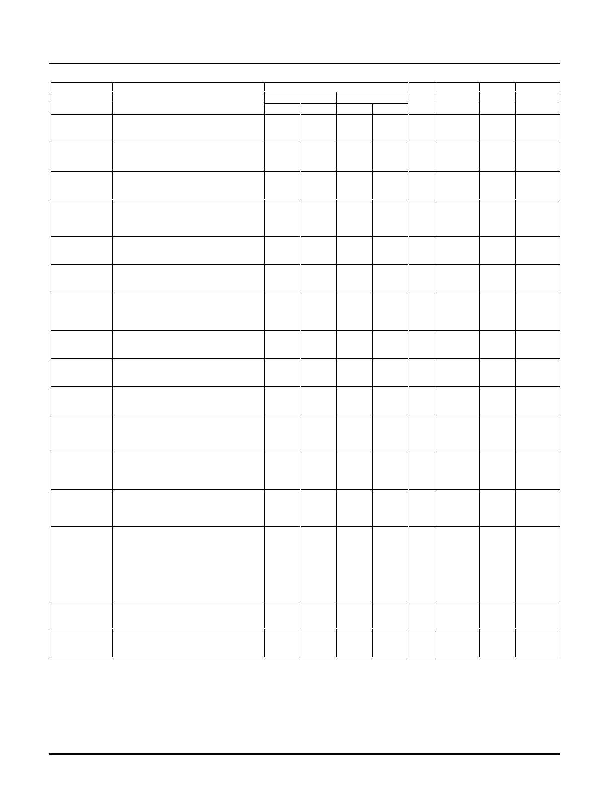
OZ6933
Name1 Description2
A22/
CTRDY#
A21/
CDEVSEL#
A20/
CSTOP#
A19/
CBLOCK#
A18/
RFU
A17/
CAD16
A16/
CCLK#
A15/
CIRDY#
A14/
CPERR#
A13/
CPAR
A12/
CCBE2#
A[11:9]/
CAD[12, 9,
14]
A8/
CCBE1#
A[7:0]/
CAD[18, 2026]
D15/
CAD8
D14/
RFU
PCMCIA socket address 22 output.
CardBus Target Ready: In CardBus
mode, this pin is the CTRDY# signal.
PCMCIA socket address 21 output.
CardBus Device Select: In CardBus
mode, this pin is the CDEVSEL# signal.
PCMCIA socket address 20 output.
CardBus Stop: In CardBus mode, this
pin is the CSTOP# signal.
PCMCIA socket address 19 output.
CardBus Lock: In CardBus mode, t his
signal is the CB LOCK# signal used for
locked transactions .
PCMCIA socket address 18 output.
Reserved: In CardBus mode, this pin is
reserved for future use.
PCMCIA socket address 17 output.
CardBus Address/Data: In CardBus
mode, this pin is t he CAD bit 16.
PCMCIA socket address 16 output.
CardBus Clock: In CardBus mode, this
pin supplies the clock to the inserted
card.
PCMCIA socket address 15 output.
CardBus Initiator Ready: In CardBus
mode, this pin is t he CIRDY# signal.
PCMCIA socket address 14 output.
CardBus Parity Error: CardBus mode,
this pin is the CPERR# signal.
PCMCIA socket address 13 output.
CardBus Parity:b In CardBus mode,
this pin is the CPAR s i gnal .
PCMCIA socket address 12 output.
CardBus Command/Byte Enable: In
CardBus mode, this pi n is the CCBE2#
signal.
PCMCIA socket address 11:9 output.
CardBus Address/Data: In CardBus
mode, these pin are the CAD bits 12, 9
and 14.
PCMCIA socket address 8 output.
CardBus Command/Byte Enable: In
CardBus mode, this pi n is the CCBE1#
signal.
PCMCIA socket address 7:0 outputs.
CardBus Address/Data: In CardBus
mode, these pins are the CA D bits 18
and 20:26.
PCMCIA socket data/0 bit 15.
CardBus Address/Data: In CardBus
mode, this pin is t he CAD bit 8.
PCMCIA socket data I/0 bit 14.
Reserved: In CardBus mode, this pin is
reserved for future use.
Pin Number
Socket A Socket B
TQFP BGA TQFP BGA
94 W14 170 A13 1 I/O-PU 2 or 3 CardBus
92 U13 168 B13 1 I/O-PU 2 or 3 CardBus
90 W13 166 C13 1 I/O-PU 2 or 3 CardBus
88 U12 164 A14 1 I/O-PU 2 or 3 CardBus
85 D11 161 C14 1 TO 2 or 3 CardBus
83 U11 158 E14 1 I/O 2 or 3 CardBus
93 V13 169 E12 1 I/O 2 or 3 CardBus
95 P13 171 C12 1 I/O-PU 2 or 3 CardBus
86 V12 162 A15 1 I/O-PU 2 or 3 CardBus
84 R11 159 C15 1 I/O 2 or 3 CardBus
97 V14 173 A12 1 I/O 2 or 3 CardBus
77, 73,
80
82 V11 157 A16 1 I/O 2 or 3 CardBus
100,
103,
105,
107,
109,
111,
113,
116
71 W9 148 F17 1 I/O 2 or 3 CardBus
69 V8 145 G17 1 I/O 2 or 3 2 mA
V10,
U9,
W11
P14,
R14,
T19,
R17,
N14,
R19,
P18,
N17
153,
149,
155
175,
178,
181,
183,
185,
187,
189,
191
F14,
F18,
F15
B11,
F11,
E10,
F10,
B9,
E9,
A8, B8
Qty I/O Pwr Drive
spec.
spec.
spec.
spec.
spec.
spec.
spec.
spec.
spec.
spec.
spec.
3 I/O 2 or 3 CardBus
spec.
spec.
8 I/O 2 or 3 CardBus
spec.
spec.
OZ6933-SF-1.7 Page 8
Page 9
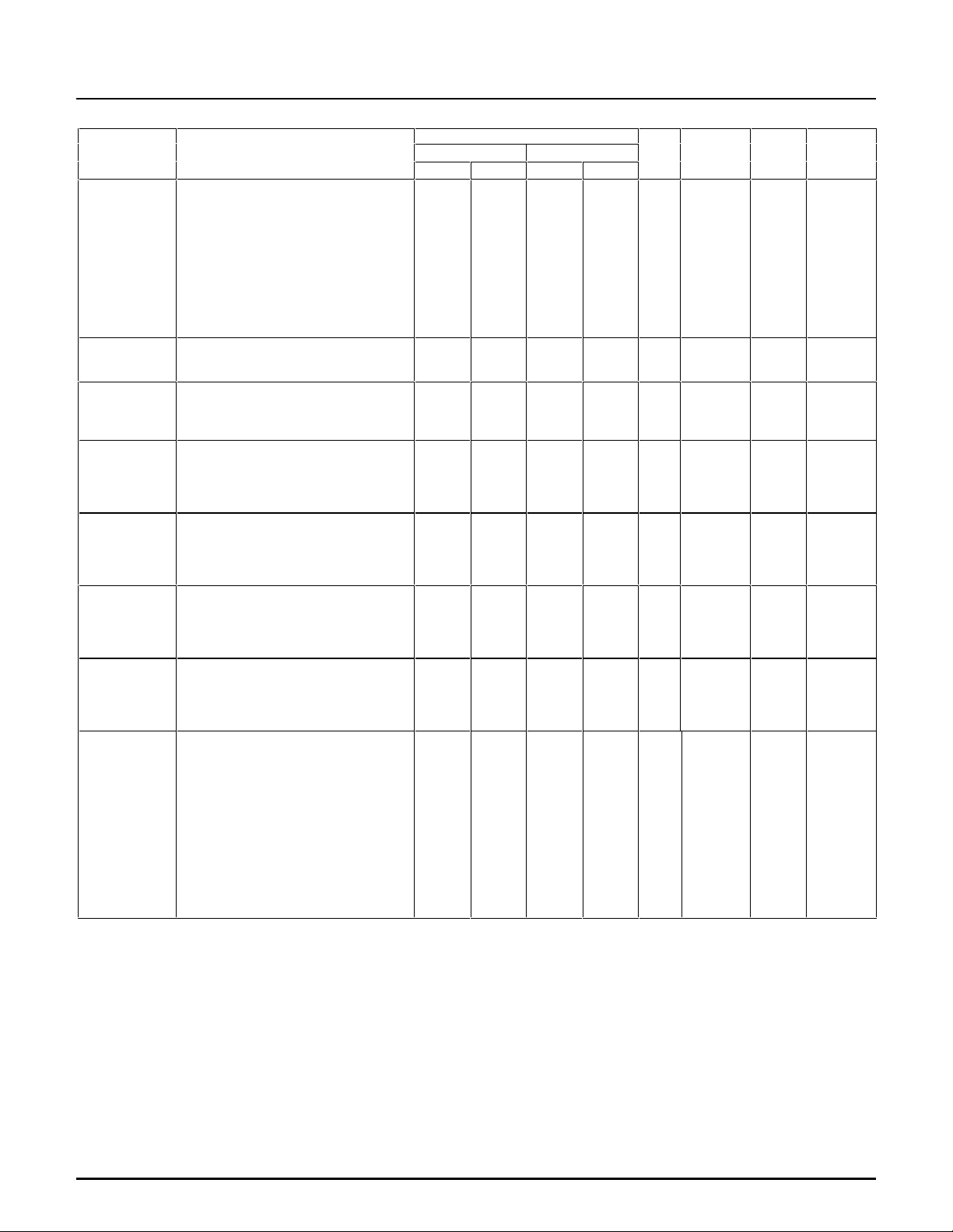
OZ6933
Name1 Description2
D[13:3]/
CAD[6, 4, 2,
31, 30, 28, 7,
5, 3, 1, 0]
D2/
RFU
D[1:0]/
CAD[29,27]
-OE/
CAD11
-WE/
CGNT#
-IORD/
CAD13
-IOWR/
CAD15
WP/
-IOIS16/
CCLKRUN#
PCMCIA socket data I/0 bits 13:3.
CardBus Address/Data: In CardBus
mode, this pin is t he CAD bit 6 4, 2, 31,
30, 28, 7, 5, 3, 1, and 0, respectively.
PCMCIA socket data I/O bit 2.
Reserved: In CardBus mode, this pin is
reserved for future use.
PCMCIA socket data I/O bits 1:0.
CardBus Address/Data: In CardBus
mode, these pins are the CA D bits 29
and 27, respectively.
Output Enable: This output goes active
(low) to indicate a memory read from
the PCMCIA socket to the OZ6933.
CardBus Address/Data: In CardBus
mode, this pin is t he CAD bit 11.
Write Enable: This out put goes active
(low) to indicate a memory write from
the OZ6933 to the PCMCIA socket.
CardBus Grant: In CardBus mode, this
pin is the CGNT# signal.
I/O Read: This output goes active (low)
for I/O reads from the socket to the
OZ6933.
CardBus Address/Data: In CardBus
mode, this pin is t he CAD bit 13.
I/O Write: This output goes active (low)
for I/O writes from the OZ6933 to the
socket.
CardBus Address/Data: In CardBus
mode, this pin is t he CAD bit 15.
Write Protect/ I/O Is 16-Bit: In Memory
Card Interface mode, this inputs is
interpreted as the status of the write
protect switch on the PCMCIA c ard. In
I/O Card Interface mode, this input
indicates the size of t he I/O data at the
current address on the PCMCIA card.
CardBus Clock Run: In CardBus
mode, this pin is the CCLKRUN# signal,
which starts and stops the CardBus
CCLK. To enable the CLKRUN# s ignal,
ExCA register 3Bh/7Bh bi t[3:2] m ust be
enabled.
Pin Number
Socket A Socket B
TQFP BGA TQFP BGA
67, 65,
63,
124,
122,
120,
68, 66,
64, 62,
59
123 L19 198 F7 1 I/O 2 or 3 CardBus
121,
119
75 P9 151 G15 1 I/O 2 or 3 CardBus
89 R12 165 E13 1 TO 2 or 3 CardBus
78 U10 154 E17 1 I/O 2 or 3 CardBus
81 P10 156 D19 1 I/O 2 or 3 CardBus
125 L17 201 A5 1 I/O-PU 2 or 3 CardBus
P8,
V7,
W6,
L18,
M19,
M15,
U8,
W7,
U7,
P8, U6
M18,
M17
142,
140,
138,
199,
197,
195,
144,
141,
139,
137,
135
196,
194
H15,
H17,
H19,
B6,
A6,
C7,
G18,
H14,
H18,
J14,
J17
B7, A7 2 I/O 2 or 3 CardBus
Qty I/O Pwr Drive
11 I/O 2 or 3 CardBus
spec.
spec.
spec.
spec.
spec.
spec.
spec.
spec.
OZ6933-SF-1.7 Page 9
Page 10
OZ6933
Name1 Description2
-INPACK/
CREQ#
RDY/
-IREQ/
CINT#
-WAIT/
CSERR#
CD[2:1]/
CCD[2:1]#
-CE2/
CAD10
-CE1/
CCBE0#
RESET/
CRST#
Input Acknowledge: The -INPACK
function is not applicable in PCI bus
environments. However, for
compatibility with other Cirrus Logic
products, this pin s hould be connected
to the PCMCIA socket’s -INPACK pin.
CardBus Request: In CardBus m ode,
this pin is the CREQ# si gnal .
Ready/Interrupt Request: In Memory
Card Interface mode, this input
indicates to the OZ6933 that t he card is
either ready or busy. In I/O Card
Interface mode, this input indicates a
card interrupt request.
CardBus Interrupt: In CardBus mode,
this pin is the CINT# signal . This signal
is active-low and level-sensit ive.
Wait: This input indicates a request by
the card to the OZ6933 to halt the c ycle
in progress until this signal is
deactivated.
CardBus System Error: In CardBus
mode, this pin is the CSERR# signal.
Card Detect: These inputs indicate to
the OZ6933 that a card is in the socket.
They are internally pulled high to the
voltage of the AuxVCC power pin.
CardBus Card Detect: In CardBus
mode, these inputs are used with
CVS[2:1] to detect presence and type of
card.
Card Enable pin is driven low by the
OZ6933 during card access cycles to
control byte/word card access. -CE1
enables even-numbered address byt es,
and -CE2 enables odd-numbered
address bytes. When configured for 8bit cards, only -CE1 is active and A0 is
used to indicate access of odd- or evennumbered bytes.
CardBus Address/Data: In CardBus
mode, this pin is t he CAD bit 10.
Card Enable pin is driven low by the
OZ6933 during card access cycles to
control byte/word card access. -CE1
enables even-numbered address byt es,
and -CE2 enables odd-numbered
address bytes. When configured for 8bit cards, only -CE1 is active and A0 is
used to indicate access of odd- or evennumbered bytes.
CardBus Command/Byte Enable: In
CardBus mode, thi s pin is t he CCBEO#
signal.
Card Reset: This output is low for
normal operation and goes high t o reset
the card. To prevent reset glitc hes to a
card, this signal is high-impedance
unless a card is seated in the socket,
card power is applied, and the card’s
interface signals are enabled.
CardBus Reset: In CardBus mode, t hi s
pin is the CRST# output.
Pin Number
Socket A Socket B
TQFP BGA TQFP BGA
110 P17 186 C9 1 I-PU 2 or 3 CardBus
91 P12 167 F12 1 I-PU 2 or 3 CardBus
108 R18 184 A9 1 I-PU 2 or 3 CardBus
126,
61
74 R9 150 E19 1 I/O 2 or 3 CardBus
70 W8 147 G14 1 I/O 2 or 3 CardBus
106 P15 182 C10 1 TO 2 or 3 CardBus
L14,
V6
202,
136
C6,
J15
Qty I/O Pwr Drive
spec.
spec.
spec.
2 I-PU-
Schmitt
1 CardBus
spec.
spec.
spec.
spec.
OZ6933-SF-1.7 Page 10
Page 11
OZ6933
Pin Number
Name1 Description2
BVD2/
-SPKR/
-LED/
CAUDIO
BVD1/
-STSCHG/
-RI/
CSTSCHG
VS2/
CVS2
VS1/
CVS1
SOCKET_VCC Connect thes e pins to the Vcc supply
1
To differentiate the sockets in the pin diagram, all socket- specific pins have either A_ or B_ prefixes to the pin names indicated.
For example, A_A[25:0] and B_A[25:0] are the independent address buses to the sockets.
2
When a socket is configured as an ATA drive interface, socket interface pin functions change.
Battery Voltage Detect 2/Speaker/
LED: In Memory Card Interface m ode,
this input serves as the BVD2 (battery
warning status) input. In I/O Card
Interface mode, this input can be
configured as a card’s -SPKR binary
audio input. For ATA or non-ATA
(SFF-68) disk-drive support, this input
can also be configured as a drivestatus LED input.
CardBus Audio: In CardBus mode,
this pin is the CAUDIO i nput.
Battery Voltage Detect 1/Status
Change/Ring Indicate: In Memory
Card Interface mode, t his input serves
as the BVD1 (battery-dead status)
input. In I/ O Card Interface m ode, this
input is the -STSCHG input, which
indicates to the OZ6933 that the card’s
internal status has changed. If bi t 7 of
the Interrupt and General Control
register is set to `1`, this pi n serves as
the ring indicate i nput for wakeup-onring system power management
support.
CardBus Status Change: In CardBus
mode, this pin is the CSTSCHG. This
pin can be used to generate PME#.
Voltage Sense 2: This pin is used in
conjunction with VS1 to det ermine the
operating voltage of the c ard. This pin
is internally pulled high t o the voltage
of the AuxVCC power pin under the
combined control of t he external data
write bits and the CD pull up control
bits. This pin connects to PCMCIA
socket pin 57.
CardBus Voltage Sense: In CardBus
mode, these pins are the CV S2 pins.
Voltage Sense 1: This pin is used in
conjunction with VS2 to det ermine the
operating voltage of the c ard. This pin
is internally pulled high t o the voltage
of the AuxVCC power pin under the
combined control of t he external data
write bits and the CD pull up control
bits. This pin connects to PCMCIA
socket pin 43.
CardBus Voltage Sense: In CardBus
mode, these pins are the CV S1 pins.
of the socket (pins 17 and 51 of the
respective PCMCIA socket). These
pins can be 0, 3. 3, or 5 V, depending
on card presence, card type, and
system configuration. The socket
interface outputs (listed in this table,
Table 2-2) will operate at the voltage
applied to these pins , independent of
the voltage applied to other OZ6933
pin groups.
Socket A Socket B
TQFP BGA TQFP BGA
114 M14 190 C8 1 I-PU 2 or 3 -
118 N19 192 F8 1 I-PU 2 or 3 -
104 W16 179 A10 1 I/O-PU 1 CB-spec
76 W10 152 E18 1 I/O-PU 1 CB-spec
60,
198
R7,
R13
200,
160,
143
E7,
F13,
G19
Qty I/O Pwr Drive
2, 3 PWR - -
OZ6933-SF-1.7 Page 11
Page 12
Power Control and General Interface Pins
Pin Name Description
SPKR_OUT
LED_OUT/
SKTA_ACTV
CPWRCLK/
A_VCC5#
CPWRDATA/
B_VCC3#
CPWRLATC/
B_VCC5#
Speaker Output: This output can be
used as a digital output to a speaker to
allow a system to support PC Card
fax/modem/voice and audio sound
output. This output is enabled by sett ing
the socket’s Misc Control 1 register bit 4
to “1” (for the socket whose speaker
signal is to be directed from BVD2/SPKR/-Led to this pin).
LED Output/SKTA_ACTV: This output
can be used as an LED driver to indicate
disk activity when a socket’s BVD2/SPKR/-LED pin has been programmed
for LED support.
In the O2 Mode(Index 3B/7B bit 5) , this
pin indicates the socket A activity. The
socket B activity refers to PCI
Configuration Register offset 90h (Mux
Control register)
Card Power Clock: This input is used as
a reference clock (10-100 kHz, usually
32 kHz) to control the serial i nterface of
the socket power control chips.
A_VCC5#: This active-LOW output
controls the 5 -volt supply to the A
socket’s VCC pins. The active-LOW
level of this output is mut ually exclusive
with that of A_VCC3#.
Card Power Serial Data: This pin
serves as output DATA pin when used
with the serial interface of Texas
Instruments’ TPS2206IDF & Micrel 2564
socket power control chip.
B_VCC3#: This active-LOW output
controls the 3.3-volt supply to the A
socket’s VCC pins. The active-LOW
level of this output is mut ually exclusive
with that of B_VCC5#.
Card Power Serial Latch: This pin
serves as output LATCH pi n when used
with the serial interface of Texas
Instruments’ TPS2206IDF & Micrel 2564
socket power control chip.
B_VCC5#: This active-LOW output
controls the 5 -volt supply to the A
socket’s VCC pins. The active-LOW
level of this output is mut ually exclusive
with that of B_VCC3#.
OZ6933
Pin Number
TQFP BGA
128 K19 TTL I/O 1 6mA
133 J19 TTL I/O 1 6mA
132 K14 TTL I/O 1 6mA
131 K15 TTL I/O 1 6mA
130 K17 N/A I/O 1 6mA
Input Type
Power
Rail
Drive
OZ6933-SF-1.7 Page 12
Page 13
Pin Name Description
IRQ3/
A_VCC3#
IRQ9/
A_VPP_VCC
IRQ10/
B_VPP_VCC
G_RST#
A_VCC3#/IRQ3: This active-LOW output
controls of the 3.3-volt supply to the
socket’s VCC pins. The active-LOW level
of this output is mutually exclusive with of
VCC_5#. This mode active only in
SktPwr Parallel mode enabled.
This pin can be IRQ3 in parallel IRQ
mode.
VPP_VCC/IRQ9: This active-HIGH
output controls the sock et A VCC supply
to the socket’s VPP1 and VPP2 pins.
The active-HIGH level of this output is
mutually exclusive with that of
VPP_PGM. This mode active only in
SktPwr Parallel mode enabled
This pin can be configured as IRQ9 in
parallel IRQ mode.
VPP_VCC/IRQ10: This active-HIGH
output controls the sock et B VCC supply
to the socket’s VPP1 and VPP2 pins.
The active-HIGH level of this output is
mutually exclusive with that of
VPP_PGM. This mode active only in
SktPwr Parallel mode enabled.
This pin can be configured as IRQ10 in
parallel IRQ mode.
Global_Reset#: This signal can be
connected to either PCI reset or ACPI
reset depending on system
implementation. If the D3 cold state is
implemented, this signal should be
connected to the ACPI res et, otherwise,
connect to PCI reset.
This signal can reset the PME content
under the D3 cold state if AUX_VCC is
provided
Power, Ground, and Reserved Pins
Pin Name Description
AUX_VCC This pin must be connected to the
CORE_VCC This pin provides power to the core
GND All OZ6933 ground pins must be
system’s 3.3-volt supply.
circuitry of the OZ6933. It must be
connected to a 3.3 power supply.
connected to system ground.
OZ6933
Pin Number
TQFP BGA
87 W12 N/A TO 1 6mA
115 P19 N/A TO 1 6mA
146 F19 N/A TO 1 6mA
117 N18 TTL I 1 -
Pin Number
TQFP BGA
127 L15 N/A PWR - -
180, 134, 79 B10, J18, R10 N/A PWR - -
14, 26, 28, 44,
57, 101, 129,
177
H3, K5, K5, P2,
W5, V15, K18,
E11
Input Type
Input Type
N/A GND -
Power
Rail
Power
Rail
Drive
Drive
-
Legend
I/O Type Description Power
I Input Pin 1 AUX_VCC: outputs powered from AUX_VCC
I-PU Input pin with internal pull-up 2 A_SLOT_VCC: outputs powered from the socket A
O Output 3 B_SLOT_VCC: outputs powered from the socket B
OD Open-drain 4 PCI_VCC: outputs powered from PCI bus power supply
TO Tri-state output
TO-PU Tri-s tate output with internal pull-up
OD-PU Open-drain output with internal pull -up
PW Power pin
OZ6933-SF-1.7 Page 13
Rail
5 CORE_VCC: outputs powered from the CORE_VCC
Source of Output’s Power
Page 14
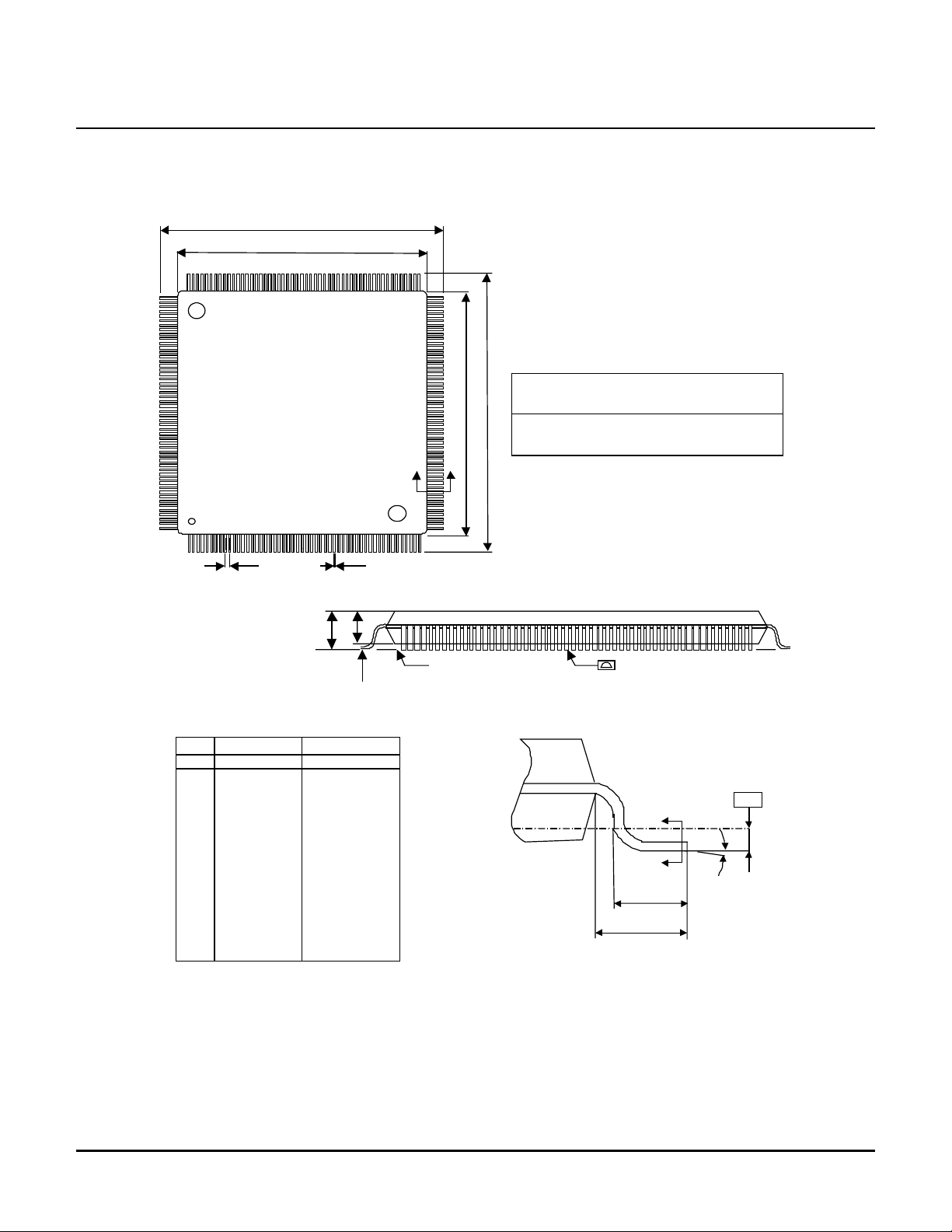
PACKAGE SPECIFICATIONS
D
D
1
156 105
OZ6933
157
208
1 52
INCHES MILLIMETERSSymbol
MIN NOM MAX MIN NOM MAX
A - - 0.063 - - 1.60
A
0.002 - 0.006 0.05 - 0.15
1
0.053 0.055 0.057 1.35 1.40 1.45
A
2
b 0.007 0.009 0.011 0.17 0.22 0.27
c 0.004 - 0.008 0.09 - 0.20
D 1.181 30.00 BSC.
D
1
E 1.181 30.00 BSC.
E
1
e 0.020 BSC. 0.50 BSC.
L 0.018 0.024 0.030 0.45 0.60 0.75
L
1
θ
1.102 28.00 BSC.
1.102 28.00 BSC.
0.039 REF 1.00 REF
0° 3.5° 7° 0° 3.5° 7°
104
OZ6933 208-PIN TQFP
1
E
E
O
MICRO, INC.
2
F F
53
be
A
A2
A1
SEATING PLANE
GAGE PLANE
SEC: F-F
0.25
B
B
L
L1
θ
OZ6933-SF-1.7 Page 14
Page 15
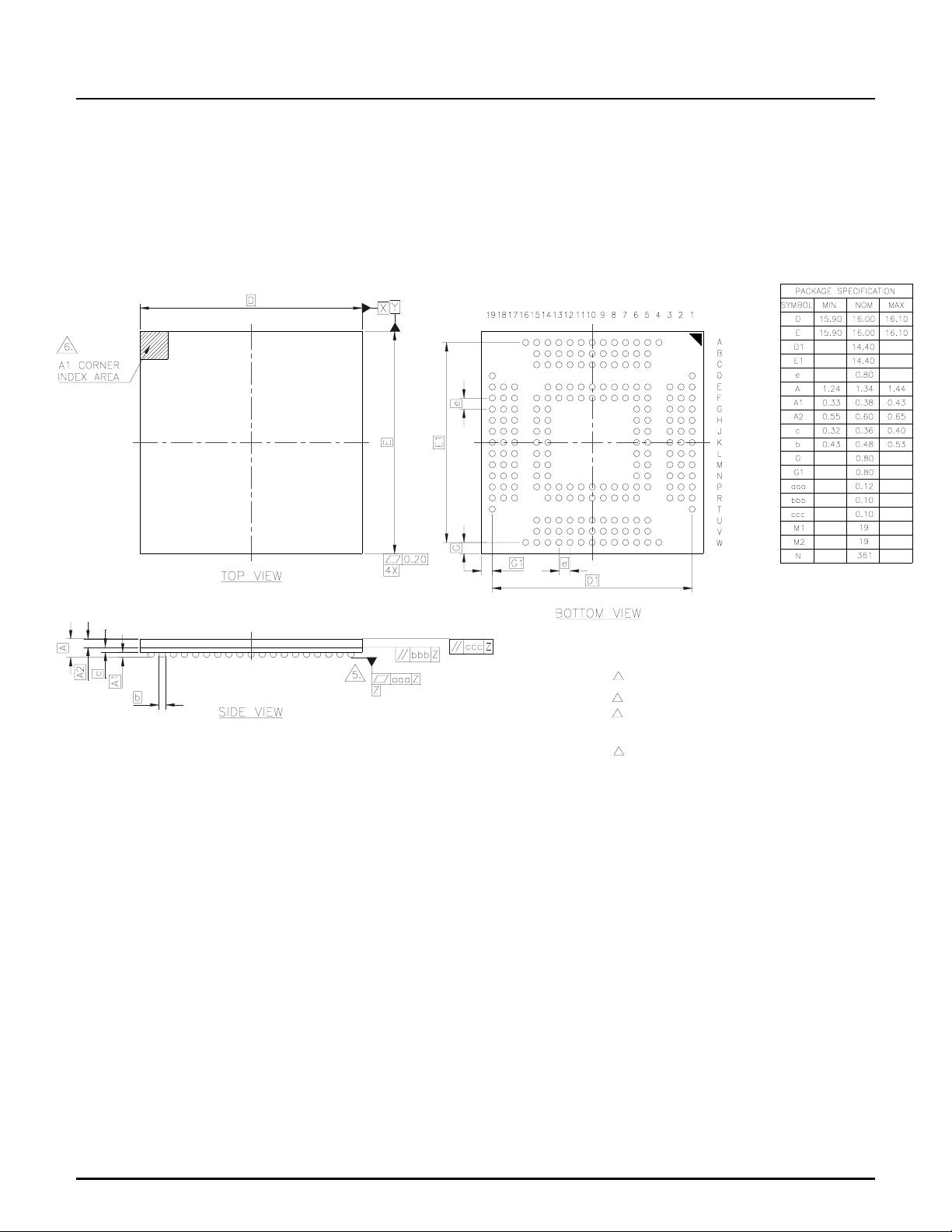
208 PIN – BGA
OZ6933
NOTES:
1. DIMENSIONING AND TOLERANCING PER ASME Y14.5M-1994.
2. "e" REPRESENTS THE SOLDER BALL GRID PITCH.
3. "N" REPRESENTS THE MAXIMUM NUMBER OF SOLDER BALLS FOR MATRIX SIZE
M1 AND M2.
4. DIMENSION "b" IS MEASURED AT THE MAXIMUM SOLDER BALL DIAMETER AFTER
REFLOW AND PARALLEL TO PRIMARY DATUM Z, THE ORIGINAL SOLDER BALL
DIAMETER IS 0.45 mm.
5. PRIMARY DATUM Z AND SEATING PLANE ARE DEFINED BY THE SPHERICAL
CROWNS OF THE SOLDER BALLS.
6. A1 CORNER MUST BE IDENTIFIED BY INK MARK, METALLIZED MARKINGS,
IDENTATION OR OTHER FEATURE OF PACKAGE BODY, LID OR INTEGRAL
HEATSLUG, ON THE TOP SURFACE OF THE PACKAGE.
7. SOLDER BALL DEPOPULATION IS ALLOWED. DEPOPULATION IS THE OMISSION OF
BALLS FROM A FULL MATRIX (M1 OR M2).
8. BALL PAD A1 CORNER INDICATOR (NC) SOLDER BALL
OZ6933-SF-1.7 Page 15
 Loading...