

Page 1
© 1994 Burr-Brown Corporation PDS-1271D Printed in U.S.A. May, 1997
DESCRIPTION
The OPA655 combines a very wideband, unity gain
stable, voltage feedback op amp with a FET input
stage to offer an ultra high dynamic range amplifier
for ADC buffering and transimpedance applications.
Extremely low harmonic distortion along with excellent pulse settling characteristics will support even the
most demanding ADC input buffer requirements.
The broad unity gain stable bandwidth and FET input
allows exceptional performance in high speed, low
noise integrators.
The high input impedance and low bias current provided by the FET input is further supported by the
ultra-low 6nV/√Hz input voltage noise to achieve a
very low integrated noise in wideband photodiode
transimpedance applications.
Broad transimpedance bandwidths are achievable given
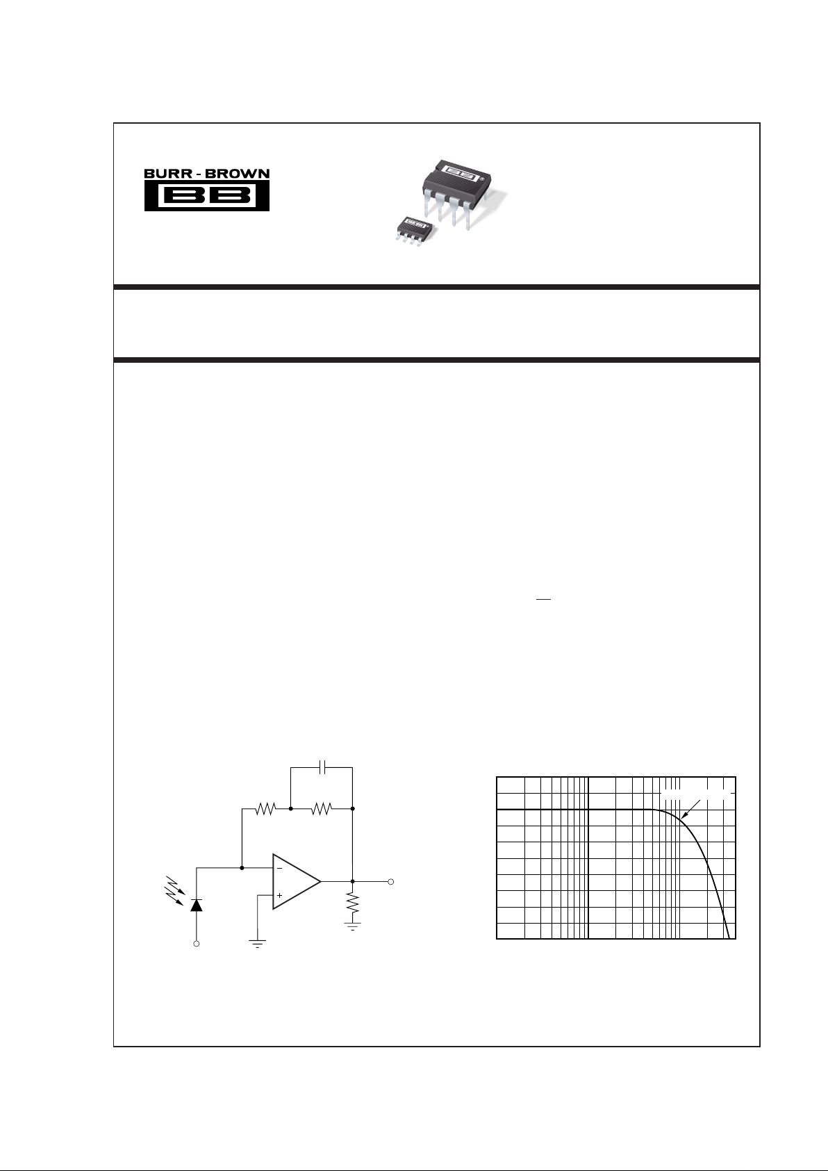
the OPA655’s high 240MHz gain bandwidth product.
As shown below, a –3dB bandwidth of 1MHz is
provided even for a high 1MΩ transimpedance gain
from a 47pF source capacitance.
FEATURES
● 400MHz UNITY GAIN BANDWIDTH
● LOW INPUT BIAS CURRENT: 5pA
● HIGH INPUT IMPEDANCE: 10
12
Ω || 1.0pF
● ULTRA-LOW dG/dP: 0.006%/0.009
°
● LOW DISTORTION: 90dB SFDR at 5MHz
● FAST SETTLING: 17ns (0.01%)
● HIGH OUTPUT CURRENT: 60mA
● FAST OVERDRIVE RECOVERY
Wideband, Unity Gain Stable, FET-Input
OPERATIONAL AMPLIFIER
OPA655
APPLICATIONS
● WIDEBAND PHOTODIODE
AMPLIFIER
● PEAK DETECTOR
● CCD OUTPUT BUFFER
● ADC INPUT BUFFER
● HIGH SPEED INTEGRATOR
● TEST AND MEASUREMENT FRONT END
®
Frequency
1MΩ TRANSIMPEDANCE BANDWIDTH
130
120
110
100
90
80
10kHz 100kHz 1MHz 5MHz
Transimpedance Gain (dB)
1MHz Bandwidth
OPA655
Wideband Photodiode Transimpedance Amplifier
(47pF)
λ
–V
b
499kΩ499kΩ
V
O
100Ω
1pF
International Airport Industrial Park • Mailing Address: PO Box 11400, Tucson, AZ 85734 • Street Address: 6730 S. Tucson Blvd., Tucson, AZ 85706 • Tel: (520) 746-1111 • Twx: 910-952-1111
Internet: http://www.burr-brown.com/ • FAXLine: (800) 548-6133 (US/Canada Only) • Cable: BBRCORP • Telex: 066-6491 • FAX: (520) 889-1510 • Immediate Product Info: (800) 548-6132
OPA655
OPA655
Page 2

®
OPA655
2
SPECIFICATIONS
At TA = +25°C, VS = ±5V, R
FB
= 100Ω, and RL = 100Ω, unless otherwise noted. R
FB
= 0 for G = +1.
OPA655P, U
PARAMETER CONDITIONS MIN TYP MAX UNITS
The information provided herein is believed to be reliable; however, BURR-BROWN assumes no responsibility for inaccuracies or omissions. BURR-BROWN assumes
no responsibility for the use of this information, and all use of such information shall be entirely at the user’s own risk. Prices and specifications are subject to change
without notice. No patent rights or licenses to any of the circuits described herein are implied or granted to any third party. BURR-BROWN does not authorize or warrant
any BURR-BROWN product for use in life support devices and/or systems.
FREQUENCY RESPONSE
Closed-Loop Response Gain = +1V/V, V
O
= 200mVp-p 400 MHz
Gain = +2V/V, V
O
= 200mVp-p 185 MHz
Gain = +5V/V, V
O
= 200mVp-p 57 MHz
Gain = +10V/V, V
O
= 200mVp-p 24 MHz
Gain-Bandwidth Product 240 MHz
Slew Rate G = +1, 1V Step 210 290 V/µs
Over Temperature 200 V/µs
Rise Time 0.2V Step 1 ns
Fall Time 0.2V Step 1 ns
Settling Time: 0.01% G = +1, 1V Step 17 ns
0.1% G = +1, 1V Step 8 ns
1% G = +1, 1V Step 6 ns
Spurious-Free Dynamic Range G = +1, f = 5MHz 75 90 dBc
V
O
= ±1V, RL = 100Ω
Differential Gain 3.58MHz, 0 to 1.4V, R
L
= 150Ω 0.006 %
Differential Phase 3.58MHz, 0 to 1.4V, R
L
= 150Ω 0.009 degrees
Bandwidth for 0.1dB flatness G = +2, 2Vp-p 30 MHz
OFFSET VOLTAGE
Input Offset Voltage ±1 ±2mV
Over Temperature ±10 µV/°C
Power Supply Rejection (+V
S
)|V
S
| = 4.50V to 5.50V 55 70 dB
(–V
S
)5065dB
INPUT BIAS CURRENT
(1)
Input Bias Current VCM = 0V –5 –125 pA
Over Temperature V
CM
= 0V –8.0 nA
Input Offset Current V
CM
= 0V ±2 ±125 pA
Over Temperature V
CM
= 0V ±8nA
NOISE
Input Voltage Noise
Noise Density: f = 100Hz 20 nV/√Hz
f = 1kHz 8 nV/√Hz
f = 10kHz 6 nV/√Hz
f = 0.1MHz to 100MHz 6 nV/√Hz
Integrated Voltage Noise,
BW = 1MHz to 100MHz 60 µVrms
Input Bias Current Noise
Current Noise Density,
f = 10Hz to 10kHz 1.3 4 fA/√Hz
INPUT VOLTAGE RANGE
Common-Mode Input Range ±2.75 V
Over Temperature ±2.5 V
Common-Mode Rejection V
CM
= ±0.5V 55 70 dB
INPUT IMPEDANCE
Differential
10
12
|| 1.2
Ω || pF
Common-Mode
10
12
|| 1.0
Ω || pF
OPEN-LOOP GAIN
Open-Loop Voltage Gain V
O
= ±2V, RL = 100Ω 53 58 dB
Over Temperature V
O
= ±2V, RL = 100Ω 50 dB
OUTPUT
Voltage Output R
L
= 100Ω, G = +1 ±3.0 ±3.4 V
Over Temperature ±2.8 V
Current Output ±35 ±60 mA
Over Temperature ±28 mA
Short-Circuit Output Current ±140 mA
Output Resistance 0.1MHz, G = +1 0.04 Ω
POWER SUPPLY
Specified Operating Voltage ±5V
Operating Voltage Range T
MIN
to T
MAX
±4.75 ±5.25 V
Quiescent Current T
MIN
to T
MAX
±21 ±25 ±29 mA
Over Temperature ±31 mA
TEMPERATURE RANGE
Specification: P, U –40 +85 °C
Thermal Resistance,
θ
JA
P 100 °C/W
U 125 °C/W
NOTE: (1) Junction temperature ≈ +25°C for room temperature tested input bias and offset current.
Page 3
3
®
OPA655
Total Supply Voltage Across Device (V
S (TOTAL)
) ................................11V
Internal Power Dissipation ........................... See Thermal Considerations
Differential Input Voltage ............................................................ V
S (TOTAL)
Common-Mode Input Voltage Range .................................................. ±V
S
Storage Temperature Range: P, U ............................... –40°C to +125°C
Lead Temperature (soldering, 10s) .............................................. +300°C
(soldering, SO-8, 3s) ...................................... +260°C
Junction Temperature (T
J
) ............................................................ +175°C
ABSOLUTE MAXIMUM RATINGS
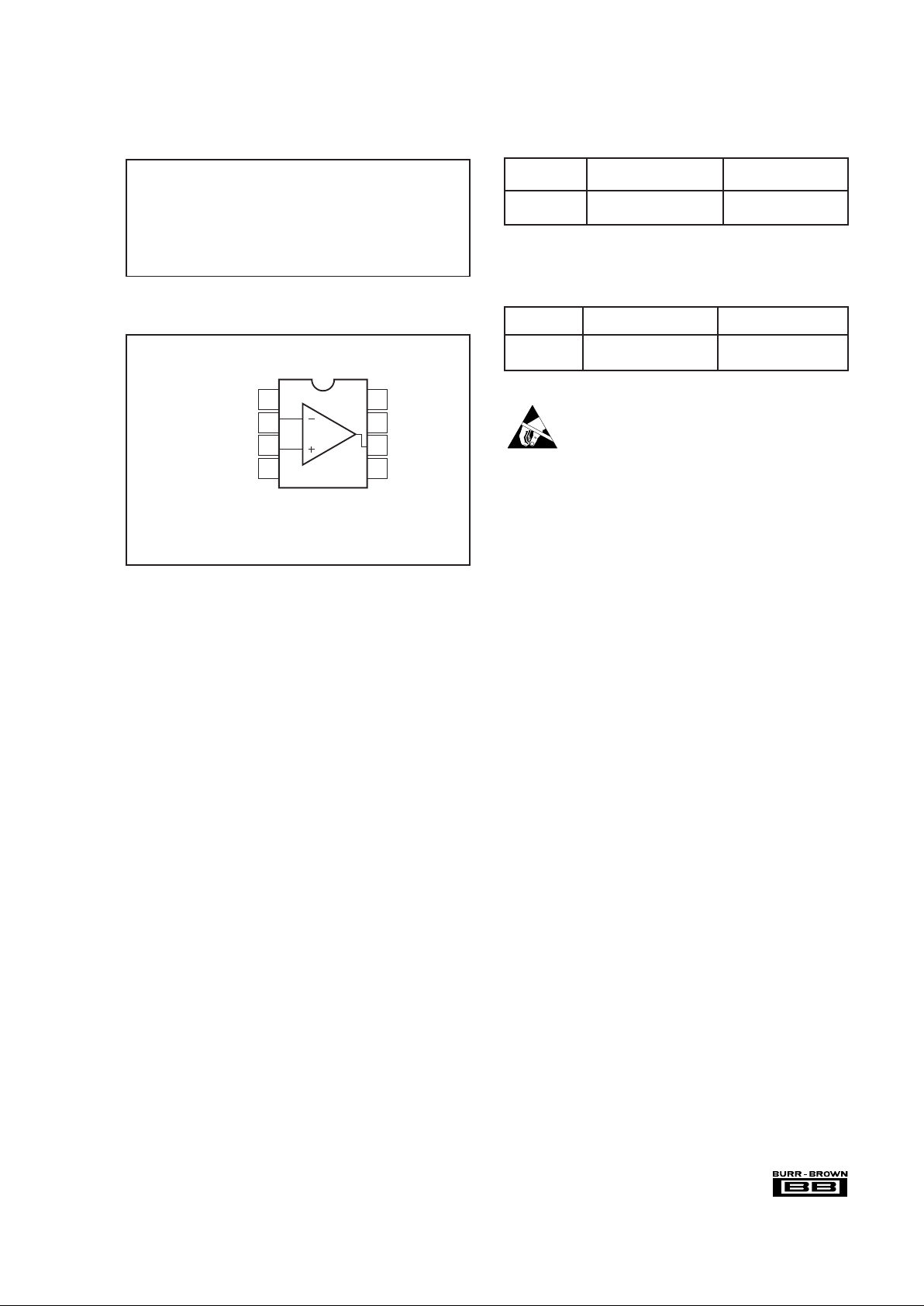
PIN CONFIGURATION
PACKAGE DRAWING
PRODUCT PACKAGE NUMBER
(1)
OPA655P 8-Pin Plastic DIP 006
OPA655U SO-8 182
NOTE: (1) For detailed drawing and dimension table, please see end of data
sheet, or Appendix C of Burr-Brown IC Data Book.
PACKAGE INFORMATION
Top View DIP/SO-8
PRODUCT PACKAGE TEMPERATURE RANGE
OPA655P 8-Pin Plastic DIP –40°C to +85°C
OPA655U SO-8 –40°C to +85°C
ORDERING INFORMATION
ELECTROSTATIC
DISCHARGE SENSITIVITY
Electrostatic discharge can cause damage ranging from performance degradation to complete device failure. Burr-Brown
Corporation recommends that all integrated circuits be handled
and stored using appropriate ESD protection methods.
ESD damage can range from subtle performance degradation
to complete device failure. Precision integrated circuits may
be more susceptible to damage because very small parametric
changes could cause the device not to meet published specifications.
NOTE: (1) Making use of all four power supply pins is highly recommended,
although not required. Using these four pins, instead of pins 4 and 7 only, will
reduce the effective pin impedance and substantially improve distortion.
1
2
3
4
8
7
6
5
+V
S2
(1)
+V
S1
Output
–V
S2
(1)
NC
Inverting Input
Non-Inverting Input
–V
S1
Page 4

®
OPA655
4
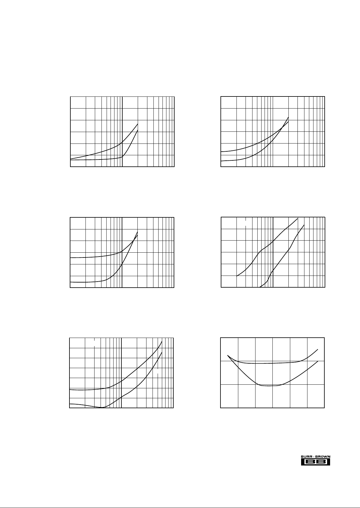
TYPICAL PERFORMANCE CURVES
At TA = +25°C, VS = ±5V, R
FB
= 100Ω, and RL = 100Ω, unless otherwise noted. R
FB
= 0 for G = +1.
INPUT VOLTAGE AND CURRENT NOISE
100
10
1
10 100 1k 10k 100k 1M 10M 100M
Input Voltage Noise (nV/√Hz)
Input Current Noise (fA/√Hz)
Frequency (Hz)
Voltage Noise
Current Noise
INPUT BIAS AND OFFSET CURRENT
vs TEMPERATURE
1000
100
10
1
–50 0 50
I
B
100
Offset Current (pA)
Input Bias Current (pA)
Temperature (°C)
IOS
CLOSED-LOOP BANDWIDTH
1M 10M 100M 1G 3G
Frequency (Hz)
6
3
0
–3
–6
–9
–12
Gain (dB)
Bandwidth
= 400MHz
SO-8DIP
G = +1
CLOSED-LOOP BANDWIDTH
100k 1M 10M 100M 1G
Frequency (Hz)
12
9
6
3
0
–3
–6
–9
–12
Gain (dB)
G = +2
DIP, SO-8
Bandwidth = 185MHz
CLOSED-LOOP BANDWIDTH
100k 1M 10M 100M 1G
Frequency (Hz)
20
17
14
11
8
5
–2
–1
–4
Gain (dB)
G = +5
DIP, SO-8
Bandwidth = 57MHz
CLOSED-LOOP BANDWIDTH
100k 1M 10M 100M 1G
Frequency (Hz)
26
23
20
17
14
11
8
5
2
Gain (dB)
G = +10
DIP, SO-8
Bandwidth = 24MHz
Page 5
5
®
OPA655
TYPICAL PERFORMANCE CURVES (CONT)
At TA = +25°C, VS = ±5V, R
FB
= 100Ω, and RL = 100Ω, unless otherwise noted. R
FB
= 0 for G = +1.
HARMONIC DISTORTION vs TEMPERATURE
(V
O
= 2Vp-p, G = +1, fO = 5MHz)
–50 –25 0 25 50 75 100
Temperature (°C)
–85
–90
–95
–100
Harmonic Distortion (dBc)
2f
O
3f
O
HARMONIC DISTORTION vs FREQUENCY
(V
O
= 2Vp-p, G = +1)
1M 10M
2f
O
3f
O
100M
Frequency (Hz)
–40
–50
–60
–70
–80
–90
–100
Harmonic Distortion (dBc)
HARMONIC DISTORTION vs FREQUENCY
(V
O
= 2Vp-p, G = +2)
1M 10M 100M
Frequency (Hz)
–40
–50
–60
–70
–80
–90
–100
Harmonic Distortion (dBc)
2f
O
3f
O
HARMONIC DISTORTION vs FREQUENCY
(V
O
= 2Vp-p, G = +5)
1M 10M 100M
Frequency (Hz)
–40
–50
–60
–70
–80
–90
–100
Harmonic Distortion (dBc)
2f
O
3f
O
5MHz HARMONIC DISTORTION
vs OUTPUT SWING
0.1 1 10
Output Swing (Vp-p)
–85
–90
–95
–100
–105
–110
–115
Harmonic Distortion (dBc)
2f
O
3f
O
G = +1
10MHz HARMONIC DISTORTION
vs OUTPUT SWING
0.1 1 10
Output Swing (Vp-p)
–60
–65
–70
–75
–80
–85
–90
–95
Harmonic Distortion (dBc)
2f
O
3f
O
G = +1
Page 6

®
OPA655
6
TYPICAL PERFORMANCE CURVES (CONT)
At TA = +25°C, VS = ±5V, R
FB
= 100Ω, and RL = 100Ω, unless otherwise noted. R
FB
= 0 for G = +1.
Time (50ns/div)
4
LARGE-SIGNAL TRANSIENT RESPONSE
Time (20ns/div)
–2
0
2
SMALL-SIGNAL TRANSIENT RESPONSE
Time (5ns/div)
0
3
2
1
0
–1
1
–1
–3
OVERDRIVE RECOVERY, G = +3
Output Voltage (V)
60
40
20
–20
–40
–60
Output Voltage (mV)
Output
Input
3
Input and Output Voltage (V)
OPEN-LOOP GAIN AND PHASE vs FREQUENCY
10 100 1k 10k 100k 1M 10M 100M 1G
Frequency (Hz)
80
60
40
20
0
–20
–40
Gain (dB)
90
45
0
–45
–90
–135
–180
Phase (°)
Gain
Phase
SUPPLY AND OUTPUT CURRENT
vs TEMPERATURE
–50 –25 0 25 50 75
I
O
I
Q
100
Temperature (°C)
28
27
26
25
24
23
Supply Current I
Q
(±mA)
80
70
60
50
40
30
Output Current I
O
(±mA)
AOL, PSR AND CMRR vs TEMPERATURE
–50 –25 0 25 50 75 100
A
OL
PSR–
PSR+
CMRR
Temperature (°C)
90
85
80
75
70
65
60
55
50
A
OL
, PSR AND CMRR (dB)
Page 7

7
®
OPA655
TYPICAL PERFORMANCE CURVES (CONT)
At TA = +25°C, VS = ±5V, R
FB
= 100Ω, and RL = 100Ω, unless otherwise noted. R
FB
= 0 for G = +1.
INPUT BIAS CURRENT
vs INPUT COMMON-MODE VOLTAGE
–3.0 –2.4 –1.8 –1.2 –0.6 0 0.6 1.2 1.8 2.4 3.0
V
CM
(V)
20
10
0
–10
–20
–30
–40
–50
–60
–70
–80
Input Bias Current I
B
(pA)
RECOMMENDED RESISTANCE
vs CAPACITIVE LOAD
0 102030405060708090100
Capacitive Load (pF)
35
30
25
20
15
10
5
R
ISO
(Ω)
G = +1
C
L
R
S
V
IN
R
ISO
COMMON-MODE REJECTION
vs INPUT COMMON-MODE VOLTAGE
–3 –2 –1 0 1 2 3
Common-Mode Voltage (V)
80
75
70
65
60
55
Common-Mode Rejection (dB)
Page 8

®
OPA655
8
DISCUSSION OF
PERFORMANCE
Amplifiers using FET input transistors operate in a similar
manner to those using bipolar transistors, with some important advantages. In standard op amp applications, the very
low input bias currents reduce the DC error voltage due to
a high or possibly unknown source impedance. In most
OPA655 applications, the output DC error will be due only
to the low 1mV input offset voltage. Similarly, input noise
currents will contribute very little to the total output noise in
most applications. Wideband transimpedance applications
(e.g., photodiode amplifiers) will particularly benefit from
the low current noise combined with the OPA655’s very low
6nV/√Hz input voltage noise.
The OPA655’s high gain bandwidth and very linear output
stage hold the harmonic distortion below –90dBc through
5MHz for a 2Vp-p swing into 100Ω. Significantly less
distortion is observed at lower frequencies and/or higher
load impedance. The voltage feedback architecture supports
this level of accuracy with greater than 65dB power supply
and common mode rejection ratios. This very high dynamic
range, along with the low DC errors and noise of the FET
input stage, can provide an exceptional buffering capability
for ADC’s, PMT’s and other applications requiring high
impedance sensing of a high speed signal. For similar
distortion performance with a bipolar input stage, refer to the
OPA642.
OPERATING CONSIDERATIONS
Careful attention to PC board layout will deliver the exceptional performance shown in the Typical Performance Curves.
Generally, very low impedance paths to the power supplies,
along with low parasitic connections to the signal I/O pins
are required for best performance (See Layout and Interconnect Considerations). Use of a guard ring around the noninverting input can reduce the leakage current due to common mode input signals. However, driving the guard from
the inverting node, can increase the differential input capacitance, possibly leading to instability or increased broadband
noise. Non-inverting buffer applications require a very low
inductance short to be connected between the output and
inverting input to minimize peaking in the frequency response. Use a wide trace (0.1") directly between the output
and inverting input pins on the component side of the board
for this connection.
The OPA655 is nominally designed to operate from ±5V
supplies. The maximum voltage between the supply pins
should be limited to less than 11V. Since a supply independent bias is used, very little change in AC performance is
observed as the supply voltage is changed.
BASIC OP AMP CONNECTIONS
Figures 2 through 4 illustrate the basic op amp connections
suitable for the OPA655. The non-inverting buffer (voltage
follower) application (Figure 2) will benefit from the very
FIGURE 1. Simplified Internal Schematic.
Current
Mirror
Supply
Independent
Bias
Output
Stage
C
C
6
+In
3
2
–In
+V
S1
Output
–V
S2
+V
S2
–V
S1
4
78
5
5Ω
5Ω
Page 9

9
®
OPA655
β = V–/V
O
Non-Inverting Gain = Noise Gain = NG = 1/β
Taking the inverting amplifier as an example, β is found by
setting V
SOURCE
to zero and calculating the voltage divider
ratio from V
O
to V–:
R
1
+ RT || RS = total resistance to ground on the
inverting input
The resulting bandwidth is approximately the amplifier’s
gain bandwidth product divided by the calculated noise gain:
BW ≈ GBW/NG
In practice, low noise gains (< 5) will produce a wider
bandwidth than predicted due to the peaking effect of second
order poles. For example, at an inverting gain of –1 from a
zero ohm source impedance, this yields a non-inverting gain
of 2 and an approximate signal bandwidth of 185MHz.
TYPICAL APPLICATIONS
WIDEBAND TRANSIMPEDANCE AMPLIFIER
The high gain bandwidth product and low noise of the
OPA655 make it particularly suitable for wideband
transimpedance applications. The front page of the data
sheet shows measured results for a 1MΩ transimpedance
gain from a relatively large diode having 47pF parasitic
capacitance. The key to broadband transimpedance applications is to set the compensation capacitance across the
feedback resistor to achieve a flat, or bandlimited, frequency
high FET input impedance and low closed loop output
impedance. Remember that a DC path to the input is still
necessary; even with the ultra low FET input bias current
(5pA), open or capacitively coupled sources will cause the
input to saturate. For best frequency response, a direct short
between the output and inverting inputs is suggested. Since
the input bias currents are not necessarily correlated, matching the non-inverting source resistance with a resistor in the
feedback network is not recommended.
FIGURE 2. Non-Inverting Unity Gain Buffer.
The non-inverting amplifier configuration (Figure 3) will
again present a very high input impedance to the input signal
and a low output impedance drive with signal gain. The
100Ω shown for R
F
will give the frequency response shown
in the Typical Performance Curves. Higher values for R
F
and R1 are possible but for high frequency non-inverting op
amp applications, should be limited to less than 1.0kΩ. The
amplifier will be loaded by (RF + R1) in parallel with the
load impedance.
V
O
RF = 100Ω
R
1
OPA655
V
IN
2
3
6
V
O
V
IN
= 1 +
R
F
R
1
FIGURE 3. Non-Inverting Op Amp.
The inverting amplifier configuration (Figure 4) offers a
broadband, low DC error amplifier with a controlled input
impedance. The input impedance may be set by adjusting R
1
to the desired value and then adjusting RF to the desired
gain, or by setting R
F
and R1 to the desired values then
controlling the input impedance independently as the parallel combination of R1 and an optional RT resistor to ground.
To estimate the bandwidth in any configuration, first calculate the gain as a non-inverting amplifier. This is often
referred to as “noise gain” or NG, and is simply the inverse
of the feedback factor β.
NG =
1
β
=1 +
R
F
R1+ RT||R
S
FIGURE 4. Inverting Op Amp.
RL = 100Ω
V
O
V
IN
V
O
= 1
6
Z
I
OPA655
2
3
V
IN
NOTE: Power supplies and de-coupling not shown.
Z
O
V
O
R
F
R
1
V
–
V
IN
R
S
R
T
V
SOURCE
2
3
6
V
O
V
IN
=
–R
F
R
1
β=
V
–
V
O
=
R
1+RT
||R
S
RF+R1+RT||R
S
Page 10

®
OPA655
10
response. Figure 5 shows the analysis circuit for setting the
feedback compensation capacitor, C
F
, while Figure 6 shows
the Bode analysis.
to set the high frequency pole for the noise gain at its
intersection with the open loop gain response.
If the 1/2πR
FCF
pole for the noise gain were set exactly at
the intersection with the amplifier’s open loop gain rolloff,
the circuit would be operating with a 45° phase margin
yielding a highly peaked frequency response. To reduce
broadband noise and pulse response ringing, it is preferable
to set this pole at a slightly lower frequency than the
simplified analysis shown above. A second order analysis
for the transimpedance configuration yields the following
results to achieve a maximally flat Butterworth characteristic for the transimpedance frequency response. Using the
OPA655’s gain bandwidth product (GBW) in Hz, define a
variable:
Then, the required CF to produce a maximally flat frequency
response is:
and the resulting –3dB bandwidth for the transimpedance
gain will be:
Figure 7 plots the required C
F
vs RF (given different values
for the diode capacitance) to achieve the maximally flat
response. Figure 8 plots the resulting bandwidth for the same
range of R
F
and CD assuming CF has been set as shown in
Figure 7. These plots include a parasitic input capacitance of
2.2pF in parallel with the diode capacitance (CD). Very low
effective values for the compensation capacitor (C
F
) can be
produced by splitting the feedback resistor as shown on the
front page application circuit.
The total capacitance to ground on the inverting input of the
OPA655 will set the source capacitance (C
S
) for analysis
purposes. C
S
is the sum of the diode capacitance (CD), the
common mode input capacitance C
CM
and the differential
input capacitance (C
DIFF
). Looking at the Bode analysis for
the transimpedance configuration, at low frequencies the
noise gain is 1 (0dB) but will increase for frequencies above
1/2π(R
F
• (CS + CF)) due to the zero formed by the capacitance on the inverting node. It is important to note that the
gain for the op amp input noise voltage will increase similarly. To get maximum bandwidth, C
F
is often set to form a
high frequency pole at the intersection of this increasing
noise gain and the open loop gain rolloff. This is accomplished by setting 1/2π(R
F
• CF) equal to the geometric mean
of the zero frequency and the gain bandwidth product of the
op amp. If the gain bandwidth product is in Hz, and assuming that C
F << CS
, CF may be calculated as:
FIGURE 5. Transimpedance Analysis Circuit.
FIGURE 6. Bode Analysis for Transimpedance Circuit.
CF=
1
R
F
•
2π • GBWP
()
R
F•CS
()
α = RF • CS • GBW • 2π (where CS = CD + CCM + C
DIFF
)
CF= CS•
2α –1
α
≈C
S
2
α
F
–3dB
= GBW •
2
α+ 2α–1
FIGURE 7. Compensation Capacitance vs Feedback
Resistance.
REQUIRED CF vs R
F
Feedback Capacitance, C
F
(pF)
10
10
1
0.1
Transimpedance Gain, R
F
(kΩ)
100 1000
CD = 200pF
CD = 20pF
CD = 10pF
CD = 100pF
CD = 50pF
OPA655
R
F
C
F
C
DIFF
C
CM
C
D
I
DIODE
A
OL
Open Loop Gain
C
S
= CD + C
DIFF
+ C
CM
Noise Gain
1
2π R
F
(CS + CF)
0
1
2π R
F CF
Gain Bandwidth
Product
f (Hz)
Page 11

11
®
OPA655
differential gain of 1.5V/V (3.5dB) to the matched load as
shown in Figure 10. The C
T
tuning capacitor is used to
match the high frequency gains for the two signal paths to
improve the high frequency CMRR. Using this adjustment,
a CMRR > 40dB through 100MHz was achieved.
HIGH SPEED INSTRUMENTATION
DIFFERENTIAL AMPLIFIER
Very high speed differential amplifiers can be implemented
using the OPA655. The very low input bias currents allow
relatively high resistor values to be used in a standard single
op amp differential configuration. Alternatively, a very high
input impedance differential amplifier can be implemented
using a three op amp instrumentation amplifier topology as
shown in Figure 9.
FIGURE 8. Maximally Flat Bandwidth.
FIGURE 9. High Input Impedance, Broadband INA.
50Ω
Load
50Ω
OPA651
V
–
V
+
R
G
100Ω
R
F
100Ω
300Ω 300Ω
R
F
100Ω
OPA655
OPA655
300Ω
C
T
1.5 to 6pF
300Ω
In this example, the OPA655’s provide a differential gain of:
and a common mode gain of 1 to the input of the OPA651
differential stage. The OPA651, a gain of 2 stable, broadband voltage feedback op amp, rejects the common mode
signal and provides a differential gain of 1/2 the matched
50Ω load. This circuit delivers a 136MHz bandwidth at a
1 +
2R
F
R
G
= 3
FIGURE 10. Measured Frequency Response for INA.
DIFFERENTIAL INPUT
3.5dB
2.5
1.5
.5
1M 10M 100M 1G
136MHz
OPTIMIZING PERFORMANCE
DC ACCURACY
The OPA655 is laser trimmed for low input offset voltage,
limiting the need for external trim circuits. In most cases, the
low bias current of the FET input will not contribute significantly to the output DC error. For example, at minimum gain
(G = +1) and maximum temperature (85°C), the error
contribution due to the inverting input bias current would
only exceed the input offset voltage for feedback resistors >
(1mV/3.2nA) = 312kΩ. Only for relatively high source and/
or feedback resistor values will the input bias current contribute significantly to the output DC error. Similarly, since
the two input bias currents are very low, but not tightly
matched, input bias current cancellation through source
impedance matching is not recommended.
Changes in the power supply voltages contribute to shifts
in the input offset voltage. This can be calculated using
the PSR specifications. For example, a 0.5V change in
the negative power supply will show up typically as a
0.5V • 10
(–65/20)
= 0.28mV change in the input offset voltage.
Negative common mode voltage inputs can cause an increase in the input bias currents as shown in the Typical
Performance Curves. This can have an effect on DC accuracy when the source and/or feedback resistors are large and
the common mode input voltage approaches the negative
limit of –2.5V. Positive input biases are therefore preferred
for diode transimpedance applications requiring a bias voltage on the non-inverting op amp input.
BANDWIDTH vs R
F
–3dB Bandwidth (MHz)
10
30
10
0.3
1
Transimpedance Gain, R
F
(kΩ)
100 1000
CD = 10pF
CD =50pF
CD = 20pF
CD = 100pF
CD = 200pF
Page 12

®
OPA655
12
FREQUENCY RESPONSE COMPENSATION
The OPA655 is internally compensated to be stable at unity
gain into a 100Ω load with a nominal phase margin of 58°.
This unity gain phase margin shows a slight peaking in the
frequency response and requires a very low inductance
shorting connection from the output pin to the inverting
input pin for minimal peaking. This stable broadband performance at unity gain lends itself well to integrator and buffer
applications.
Phase margin and flatness will improve at higher gains.
Since phase margin is slightly load dependent, flatness in a
gain of +2 can be modified by changing the loading. Very
flat performance is shown in the Typical Performance Curves
using a 100Ω feedback and 100Ω load. This may be peaked
up by increasing the load or feedback resistors or rolled off
by decreasing them. Recall that an inverting gain of –1 is
equivalent to a gain of +2 for bandwidth purposes, i.e. noise
gain equal to 2. The external compensation techniques
developed for voltage feedback op amps can be applied to
this device. For example, in the non-inverting configuration,
placing a capacitor across the feedback resistor will reduce
the gain to +1 starting at f = 1/(2π R
F CF
) Hz. Alternatively,
in the inverting configuration, the bandwidth may be limited
without modifying the low frequency inverting gain by
placing a series RC network to ground on the inverting node.
This has the effect of increasing the noise gain at higher
frequencies, thereby limiting the bandwidth for the inverting
input signal through the gain-bandwidth product.
At higher gains, the gain-bandwidth product (240MHz) of
this voltage feedback topology will limit the achievable
signal bandwidth. If FET input is not required and higher
bandwidths at higher gains are needed, consider the broad
bandwidth available from a current feedback op amp such as
the OPA658.
DRIVING CAPACITIVE LOADS
The high open loop gain and Class AB output stage of the
OPA655 are optimized for driving the low impedance of
doubly terminated cables. Capacitive loads directly on the
output pin can decrease phase margin leading to frequency
response peaking and possibly sustained oscillations. This
effect is particularly pronounced at unity gain and becomes
less significant at higher gains. Frequency response flatness
can be maintained into a capacitive load by isolating it with
a resistor as shown in Figure 11. The Typical Performance
Curves show a plot of the minimum value for R
ISO
to hold
a flat frequency response as C
L
is increased. The 1kΩ shunt
load across C
L
shown in Figure 11 was the probe load for
this measurement and should be considered optional.
PULSE AND OVERDRIVE PERFORMANCE
High speed amplifiers like the OPA655 can provide an
extremely fast settling time for a pulse input. Excellent
frequency response flatness and phase linearity are required
to get the best settling times. As shown in the specifications
table, settling time for a 1V step at a gain of +1 for the
OPA655 is an extremely fast 8ns to 0.1%. This specification
is defined as the time required, after the input transition, for
the output to settle within a specified error band around its
final value. For a 1V step, 0.1% settling corresponds to an
error band of ±1mV. For the best settling times, little or no
peaking in the frequency response can be allowed. Using the
recommended R
ISO
for capacitive loads will limit this peaking and reduce the settling times. Fast, extremely fine scale
settling (0.01%) requires close attention to the ground return
currents in the supply de-coupling capacitors. De-coupling
the output stage power supply connections (+VS2 + (–VS2))
separately from the main supply inputs will improve both
settling and harmonic distortion performance.
As can be observed in the typical performance curves, the
OPA655 recovers very quickly from an input overdrive. For
non-inverting operation, recovery is immediate for negative
overdrives and < 10ns for a positive going overdrive signal.
For inverting mode operation, such as transimpedance amplifiers, recovery is immediate to input overdrives that do
not build up input voltages that exceeds the common mode
input range. Unlike older FET input amplifiers, overdriving
the inputs does not cause the output to invert phase and/or
latch. Inputs that exceed the positive supply voltage will,
however, cause the output to reverse and swing negative—
but no latching will occur.
HARMONIC DISTORTION
The Typical Performance Curves show the very low harmonic distortion that OPA655 can deliver into a 100Ω load
over a wide range of operating conditions. Generally, distortion improves at lower gains, lower signal swings, lower
frequencies, and higher loads. Figure 12 shows significant
improvement in second harmonic distortion as the load is
increased, and relative insensitivity of the third harmonic to
load conditions. For measurement purposes, these distortion
levels were increased from those listed in the specification
table by increasing the gain to +5. Narrowband communications systems will benefit from the very low third order
distortion vs load which will provide very low intermodulation
spurs.
FIGURE 11. Driving a Capacitive Load.
1kΩ C
L
OPA655
R
ISO
R
IN
V
IN
Page 13

13
®
OPA655
THERMAL CONSIDERATIONS
The OPA655 will not require heatsinking under most operating conditions. Maximum desired junction temperature
will limit the maximum allowed internal power dissipation
as described below. In no case should the maximum junction
temperature be allowed to exceed +175°C.
Operating junction temperature (T
J
) is given by
T
A
+ PD •
θ
JA
. The total internal power dissipation (PD) is a
combination of the quiescent power plus the power dissipated in the output stage to deliver load power. Quiescent
power is simply the specified no-load supply current times
the total supply voltage across the part. P
DL
will depend on
the required output signal and load but would, for a grounded
resistive load, be at a maximum when the output is a
fixed DC voltage equal to 1/2 of either supply voltage
(assuming equal bipolar supplies). Under this condition
P
DL
= V
S
2
/(4 • RL) where RL includes feedback network
loading. Note that it is the power dissipated in the output
stage and not in the load that determines internal power
dissipation. As an example, compute the maximum T
J
for
the OPA655U at G = +2, R
L
= 100Ω, RF = 100Ω, ±VS =
±5V, and at the specified maximum T
A
= 85°C. PD = 10V
• 31mA + (5
2
)/[4 • (100 || 200)] = 404mW. Maximum TJ =
85°C + 0.404W • 125°C/W = 136°C.
LAYOUT AND INTERCONNECT
CONSIDERATIONS
Achieving optimum performance with a high frequency
amplifier like the OPA655 requires careful attention to
layout parasitics and selection of external components. Suggestions include:
• Minimize parasitic capacitance to any AC ground for all
of the signal I/O pins. Parasitic capacitance on the output
and inverting input pins can cause instability; on the noninverting input it can react with the source impedance to
cause unintentional bandlimiting. To reduce unwanted
capacitance, a window around the signal I/O pins should
be opened in all of the ground and power planes. Otherwise, ground and power planes should be unbroken elsewhere on the board.
• Minimize the distance (< 0.25") from the four power pins
to high frequency 0.1µF decoupling capacitors. At the
pins, the ground and power plane layout should not be in
close proximity to the signal I/O pins. The OPA655 may
be operated with only pins 4 and 7 connected as supply
pins allowing a direct replacement into existing 8 pin op
amp pinouts. Connecting the output stage power pins
separately, and decoupling them, will give the best distortion and settling performance. Avoid narrow power and
ground traces to minimize inductance between the pins
and the decoupling capacitors. Larger (2.2µF to 6.8µF)
decoupling capacitors, effective at lower frequencies,
should also be used. These may be placed somewhat
farther from the device and may be shared among several
devices in the same area of the PC board.
DIFFERENTIAL GAIN AND DIFFERENTIAL PHASE
The OPA655 provides one of the lowest dG/dP errors of any
op amp. This specification is the change in the small signal
gain and phase for a composite video color carrier frequency
when the output voltage is slowly ramped over the luminance range. The specifications show less than 0.01%/0.01°
for positive NTSC into a single video load. This level of
performance challenges the accuracy of commercially available video test equipment. Measurements were taken using
an HP9480 IC parametric test system.
OUTPUT DRIVE CAPABILITY
The guaranteed output current of ±28mA will drive a 100Ω
load over the full guaranteed output voltage range of ±2.8V.
These minimum performance levels are only applicable at
cold temperatures, with higher output voltage and current
available in most applications. Many demanding high speed
applications, such as driving ADC’s, require amplifiers with
low, broadband, output impedance. As shown in Figure 13,
the OPA655 maintains a very low closed loop output impedance over frequency. Closed loop output impedance increases with frequency as the loop gain rolls off.
FIGURE 12. 5MHz Harmonic Distortion vs Load Resistance.
–50
–60
–70
–80
–90
–100
10 100 1000
Load Resistance (Ω)
Harmonic Distortion (dBc)
2f
O
3f
O
VO = 2Vp-p, G = +5, fO = 5MHz
FIGURE 13. Small-Signal Output Impedance vs Frequency.
10
1
0.01
0.1
0.001
10k 100k 1M 10M 100M
Frequency (Hz)
Output Impedance (Ω)
G = +1
Page 14

®
OPA655
14
• Careful selection and placement of external compo-
nents will preserve the high frequency performance of
the OPA655. Resistors should be a very low reactance
type. Surface mount resistors work best and allow a tighter
overall layout. Metal film or carbon composition axiallyleaded resistors can also provide good high frequency
performance. Again, keep their leads as short as possible.
Never use wirewound type resistors in the signal path for
a high frequency application. For the lowest parasitic
capacitance, consider the PR8351 style resistor from Precision Resistive Products (Phone No. 319-394-9131). These
precision buffed resistors typically have less than 0.02pF
shunt parasitic capacitance.
Since the output pin and inverting input pin are most
sensitive to parasitic capacitance, always place the feedback, gain setting, and series output resistor (if any) as
close as possible to the package pins. For a voltage
follower buffer application, a wide trace (0.1") on the
component side of the board between pins 6 and 2 will
reduce frequency response peaking. Be sure to open up
ground and power planes around this trace to limit parasitic capacitance to an AC ground on the output pin.
• Connections to other wideband devices on the board
may be made with short direct traces or through on-board
transmission lines. For short connections, consider the
trace and the input to the next device as a lumped capacitive load. Relatively wide traces (50 to 100mils) should be
used, preferably with ground and power planes opened up
around them. Estimate the total capacitive load and set
R
ISO
from the plot of recommended R
ISO
vs capacitive
load. Low parasitic loads may not need an R
ISO
since the
OPA655 is nominally compensated to operate with a 5pF
parasitic load.
If a long trace is required and the 6dB signal loss intrinsic
to doubly terminated transmission lines is acceptable,
implement a matched impedance transmission line using
microstrip or stripline techniques (consult an ECL design
handbook for microstrip and stripline layout techniques).
A 50Ω environment is not necessary on board, and in fact
a higher impedance environment will improve distortion
as shown in the distortion vs load plot. With a characteristic impedance defined based on board material and
desired trace dimensions, a matching series resistor into
the trace from the output of the amplifier is used as well
as a terminating shunt resistor at the input of the destination device; the total effective impedance should match
the trace impedance. Multiple destination devices are best
handled as separate transmission lines, each with their
own series and shunt terminations.
• Socketing a high speed part like the OPA655 is not
recommended. The additional lead length and pin-to-pin
capacitance introduced by the socket creates an extremely
troublesome parasitic network which can make it impossible to achieve a smooth, stable response. Best results are
obtained by soldering the part onto the board. If socketing
for the DIP package is desired, high frequency flush
mount pins (e.g. McKenzie Technology No. 710C) can
give good results.
SPICE MODEL AND EVALUATION BOARDS
Computer simulation of circuit performance using SPICE is
often useful when analyzing the performance of analog
circuits and systems. This is particularly true for Video and
RF amplifier circuits where parasitic capacitance and inductance can have a major effect on circuit performance. SPICE
models are available on a disk from the Burr-Brown Applications Department.
The OPA655 is similar in distortion performance and identical in pinout to the OPA642. The demonstration boards
developed for the OPA642 are recommended for the OPA655.
The six boards available are:
Contact your local Burr-Brown sales office or distributor to
order demonstration boards.
DEM-OPA64XP-F 8-pin DIP, unity gain follower configuration
DEM-OPA64XP-N 8-pin DIP, non-inverting gain configuration
DEM-OPA64XP-I 8-pin DIP, inverting gain configuration
DEM-OPA64XU-F SO-8 Surface Mount, unity gain follower configuration
DEM-OPA64XU-N SO-8 Surface Mount, non-inverting gain configuration
DEM-OPA64XU-I SO-8 Surface Mount, inverting gain configuration
 Loading...