

Page 1
®
OPA671
Wide Bandwidth, Fast Settling
Difet
®
OPERATIONAL AMPLIFIER
OPA671
FEATURES
● HIGH GAIN-BANDWIDTH: 35MHz
● LOW INPUT NOISE: 10nV/√Hz
● HIGH SLEW RATE: 100V/µs
● FAST SETTLING: 240ns to 0.01%
● FET INPUT: I
= 50pA max
B
● HIGH OUTPUT CURRENT: 50mA
● WIDE SUPPLY RANGE: V
±4.5 to ±18V
=
S
APPLICATIONS
● HIGH-SPEED DATA ACQUISITION
● OPTOELECTRONICS
● TRANSIMPEDANCE AMPLIFIER
● LINE DRIVER
● CCD BUFFER AMPLIFIER
Trim
1
Trim
5
DESCRIPTION
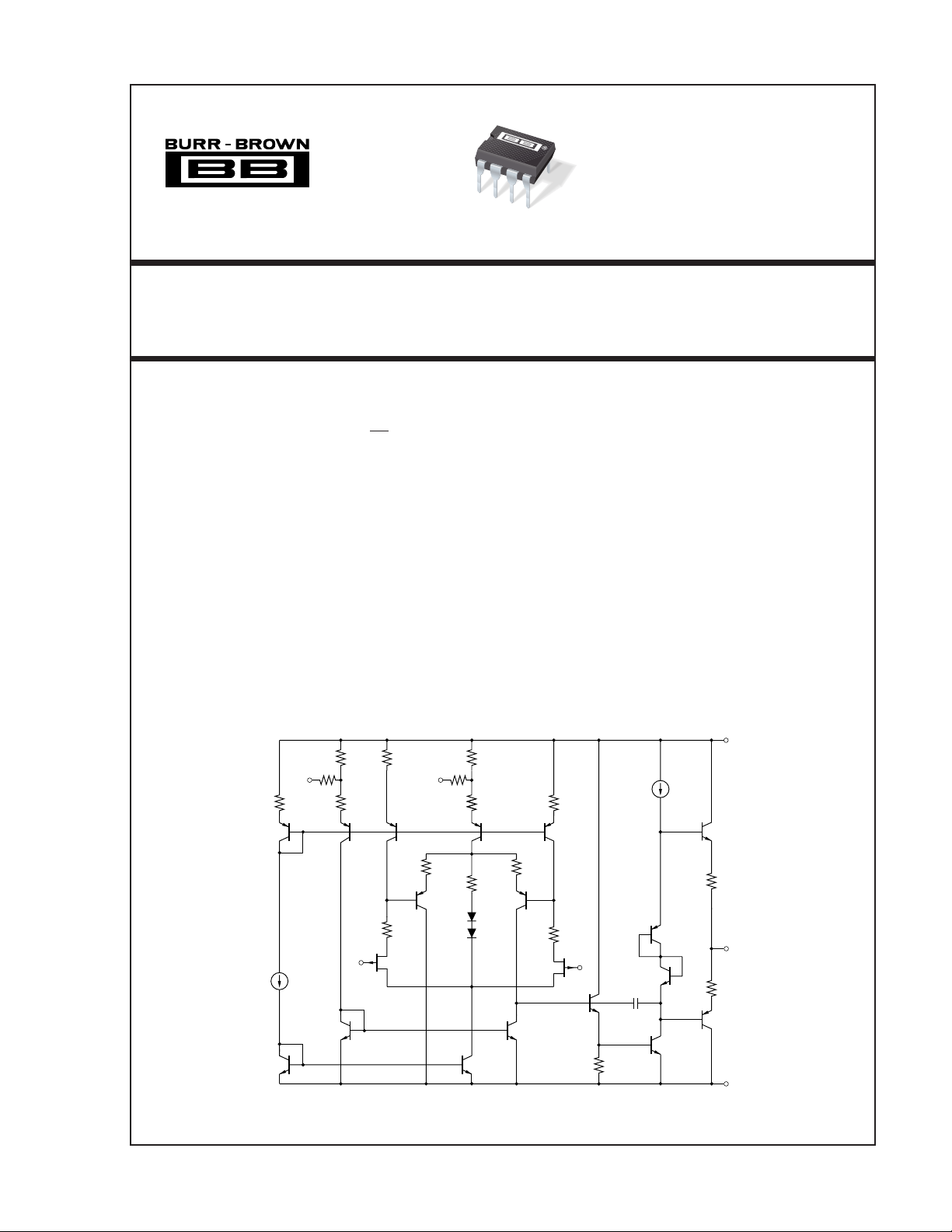
The OPA671 is a FET-input monolithic operational
amplifier featuring wide bandwidth and fast settling
time. Fabricated using Burr-Brown’s
mentary bipolar process, it provides an excellent combination of high speed, accuracy, and high output
current.
The OPA671 is versatile, operating from ±4.5V to
±18V power supplies. It can deliver ±10V signals into
a 200Ω load at slew rates of 100V/µs. OPA671’s
input provides input bias current thousands of times
lower than bipolar-input wideband op amps.
The OPA671 is internally compensated to be unity-gain
stable, allowing use in the widest range of applications.
The OPA671 is available in an 8-pin plastic DIP, rated
for the industrial temperature range.
Difet
, comple-
Difet
V+
7
V
+In
3
®
Difet
Burr-Brown Corporation
International Airport Industrial Park • Mailing Address: PO Box 11400, Tucson, AZ 85734 • Street Address: 6730 S. Tucson Blvd., Tucson, AZ 85706 • Tel: (520) 746-1111 • Twx: 910-952-1111
Internet: http://www.burr-brown.com/ • FAXLine: (800) 548-6133 (US/Canada Only) • Cable: BBRCORP • Telex: 066-6491 • FAX: (520) 889-1510 • Immediate Product Info: (800) 548-6132
© 1991 Burr-Brown Corporation PDS-1120D Printed in U.S.A. October, 1993
–In
2
O
6
4
V–
Page 2
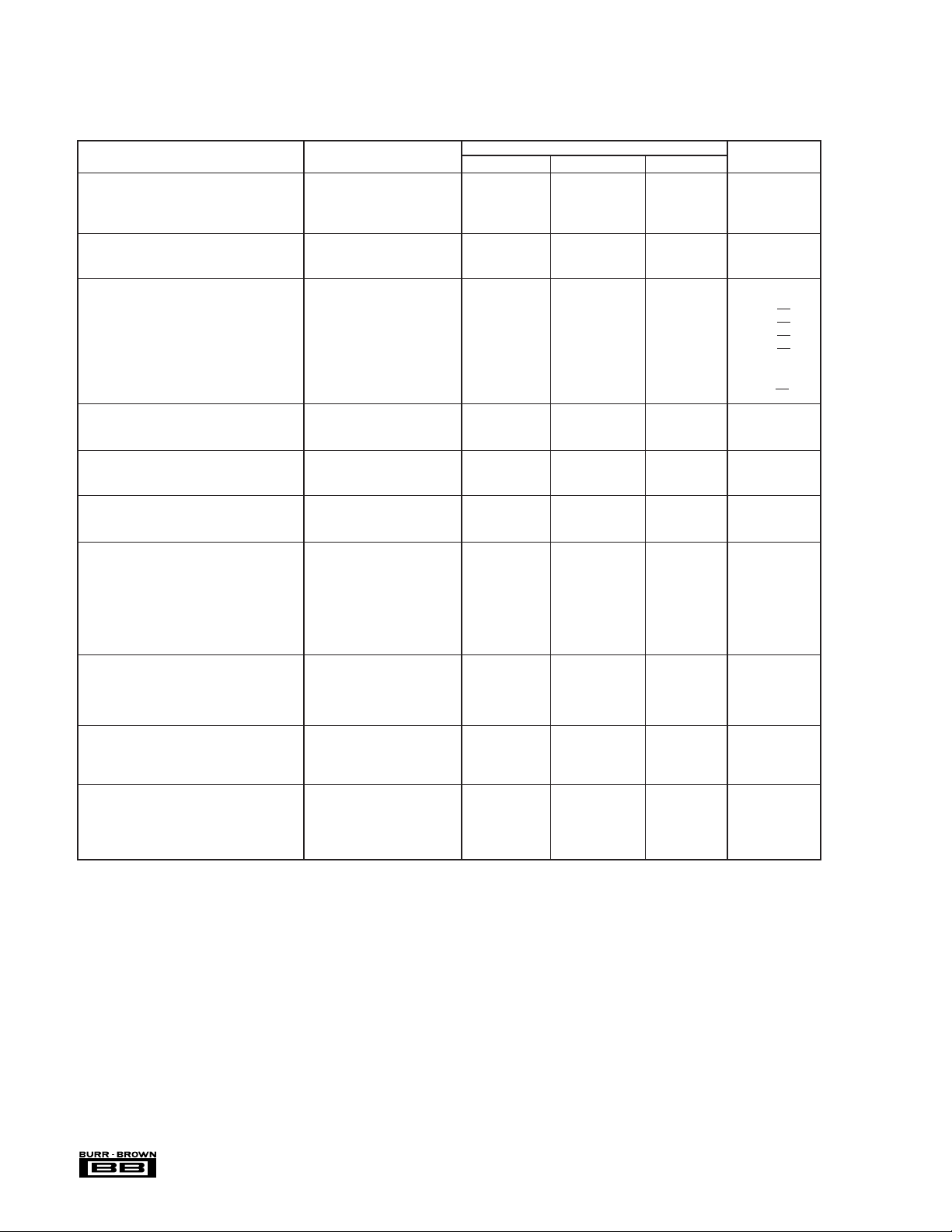
SPECIFICATIONS
At TA = +25°C, VS = ±15V, unless otherwise noted.
OPA671AP
PARAMETER CONDITION MIN TYP MAX UNITS
OFFSET VOLTAGE
Input Offset Voltage ±0.5 ±5mV
Average Drift ±10 µV/°C
Power Supply Rejection V
INPUT BIAS CURRENT
(1)
Input Bias Current V
Input Offset Current V
NOISE
Input Voltage Noise
Noise Density, f = 100Hz 24 nV/√Hz
f = 1kHz 15 nV/√Hz
f = 10kHz 12 nV/√Hz
f = 100kHz 10 nV/√Hz
Voltage Noise, BW = 10Hz to 1MHz 60 µVp-p
Input Bias Current Noise
Current Noise Density, f = 10Hz to 1MHz 2 fA/√Hz
INPUT VOLTAGE RANGE
Common-Mode Input Range ±12 ±13 V
Common-Mode Rejection V
INPUT IMPEDANCE
Differential 10
Common-Mode 10
OPEN-LOOP GAIN
Open-Loop Voltage Gain V
FREQUENCY RESPONSE
Gain-Bandwidth Product 35 MHz
Slew Rate G = –1, 10V Step 107 V/µs
Settling Time 0.01% G = –1, 10V Step 240 ns
0.1% G = –1, 10V Step 150 ns
1% G = –1, 10V Step 85 ns
Total Harmonic Distortion G = 1, f = 100kHz 0.0006 %
OUTPUT
Voltage Output R
Current Output V
Short Circuit Current –90/+105 mA
Output Resistance, Open-Loop DC 20 Ω
POWER SUPPLY
Specified Operating Voltage ±15 V
Operating Voltage Range ±4.5 ±18 V
Quiescent Current V
TEMPERATURE RANGE
Specification –25 +85 °C
Operating –40 +100 °C
Storage –40 +125 °C
Thermal Resistance,
NOTE: (1) Tested without warm-up at T
θ
JA
= TA = 25°C.
J
= ±4.5 to ±16.5V 72 94 dB
S
= 0V 5 50 pA
CM
= 0V 2 pA
CM
= ±10V 74 92 dB
CM
12
|| 4.5 Ω || pF
12
|| 6 Ω || pF
= ±10V, RL = 1kΩ 80 dB
O
V
= ±10V, RL = 200Ω 74 78 dB
O
V
= 3V, RL = 200Ω
O
= 200Ω±10.5 ±11.5 V
L
= ±10V 50 mA
O
= ±15V ±14.8 ±17 mA
S
Junction to Ambient 100 °C/W
The information provided herein is believed to be reliable; however, BURR-BROWN assumes no responsibility for inaccuracies or omissions. BURR-BROWN assumes
no responsibility for the use of this information, and all use of such information shall be entirely at the user’s own risk. Prices and specifications are subject to change
without notice. No patent rights or licenses to any of the circuits described herein are implied or granted to any third party. BURR-BROWN does not authorize or warrant
any BURR-BROWN product for use in life support devices and/or systems.
®
OPA671
2
Page 3
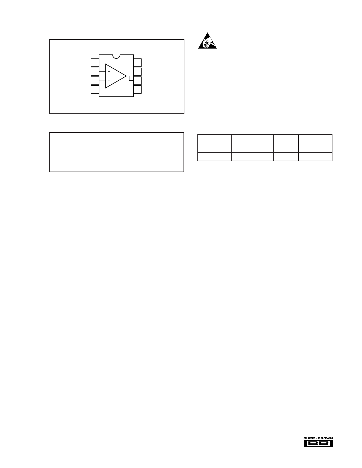
PIN CONFIGURATION
Top View DIP
ELECTROSTA TIC
DISCHARGE SENSITIVITY
VOS Trim
–In
+In
V–
1
2
3
4
NC = No Internal Connection
8
7
6
5
NC
V+
V
O
VOS Trim
ABSOLUTE MAXIMUM RATINGS
Power Supply Voltage........................................................................ ±18V
Input Voltage.............................................................(V+) +1V to (V–) –1V
Operating Temperature................................................... –40°C to +100°C
Storage Temperature ...................................................... –40°C to +125°C
Output Short-Circuit to Ground ............................................................ 15s
Junction Temperature .................................................................... +150°C
Lead Temperature (soldering, 10s)................................................ +300°C
An integrated circuit can be damaged by ESD. Burr-Brown
recommends that all integrated circuits be handled with
appropriate precautions. Failure to observe proper handling
and installation procedures can cause damage.
ESD damage can range from subtle performance degradation
to complete device failure. Precision integrated circuits may
be more susceptible to damage because very small parametric
changes could cause the device not to meet published
specifications.
PACKAGE/ORDERING INFORMATION
PACKAGE
DRAWING TEMPERATURE
PRODUCT PACKAGE NUMBER
OPA671AP 8-Pin Plastic DIP 006 –25°C to +85°C
NOTE: (1) For detailed drawing and dimension table, please see end of data
sheet, or Appendix C of Burr-Brown IC Data Book.
(1)
RANGE
®
3
OPA671
Page 4
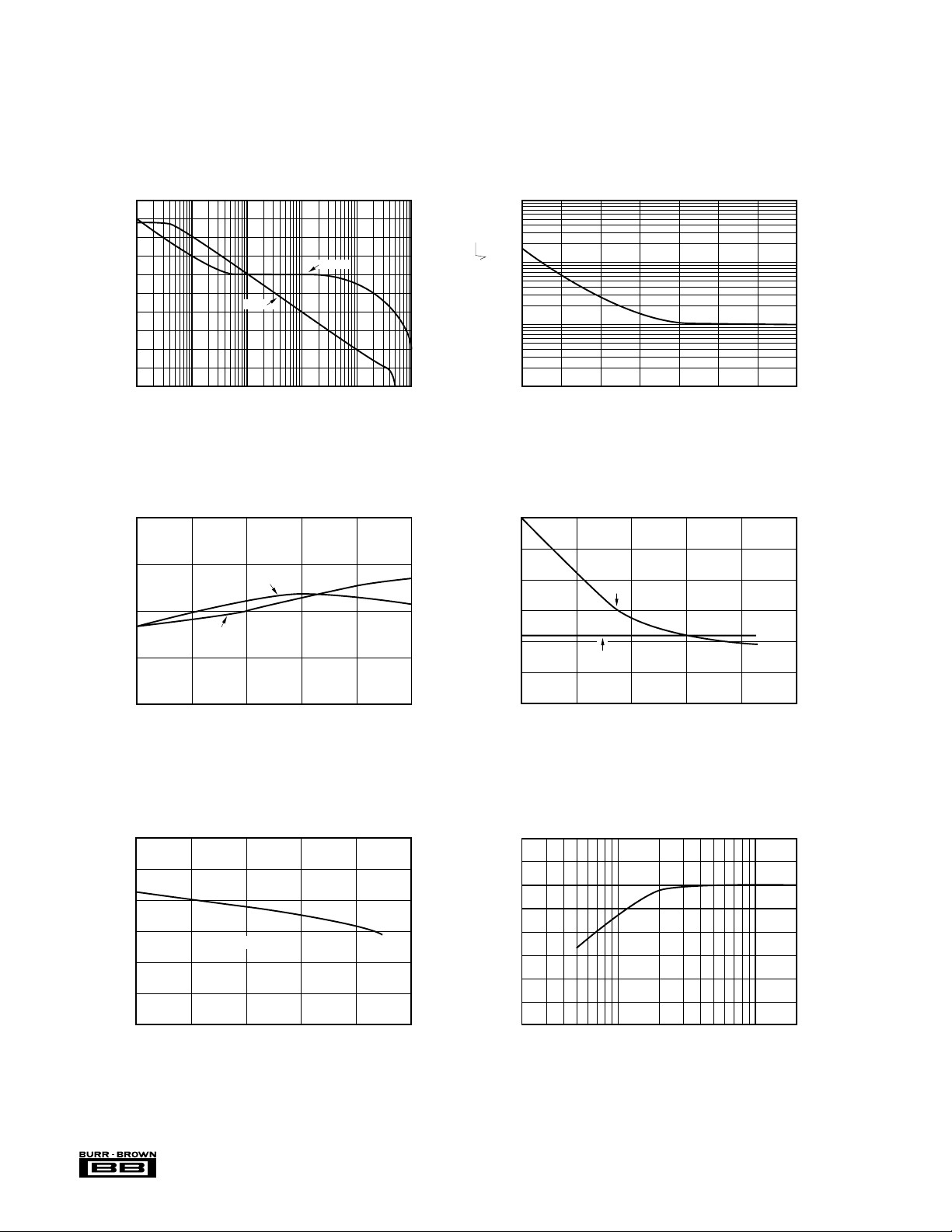
TYPICAL PERFORMANCE CURVES
TA = +25°C, VS = ±15V unless otherwise noted.
OPEN-LOOP GAIN AND PHASE
90
80
70
60
50
40
Gain (dB)
30
20
10
0
–10
1k
45
40
35
30
Gain-Bandwidth Product (MHz)
10k
GAIN-BANDWIDTH PRODUCT AND
SLEW RATE vs TEMPERATURE
GBW
vs FREQUENCY
Gain
100k
Frequency (Hz)
1M
SR
Phase
10M 100M
0
–45
–90
–135
–180
115
110
105
100
1k
100
Phase (°)
10
Voltage Noise (nV/ Hz)
0
1
110
100
Slew Rate (V/µs)
PSR & CMR (dB)
90
INPUT VOLTAGE NOISE SPECTRAL DENSITY
10k
100
10
POWER SUPPLY REJECTION AND
COMMON-MODE REJECTION vs TEMPERATURE
1k
Frequency (Hz)
PSR
CMR
100k
1M 10M
25
–25
90
80
70
Open-Loop Gain (dB)
60
–25
OPEN-LOOP GAIN vs TEMPERATURE
0
0
25
Temperature (°C)
RL = 200Ω
25
Temperature (°C)
80
50
50
75 100
75 100
–25
90
80
70
Open-Loop Gain (dB)
60
50
OPEN-LOOP GAIN vs LOAD RESISTANCE
20
0
100
Load Resistance (Ω)
25
Temperature (°C)
50
200
75 100
1k
2k
®
OPA671
4
Page 5
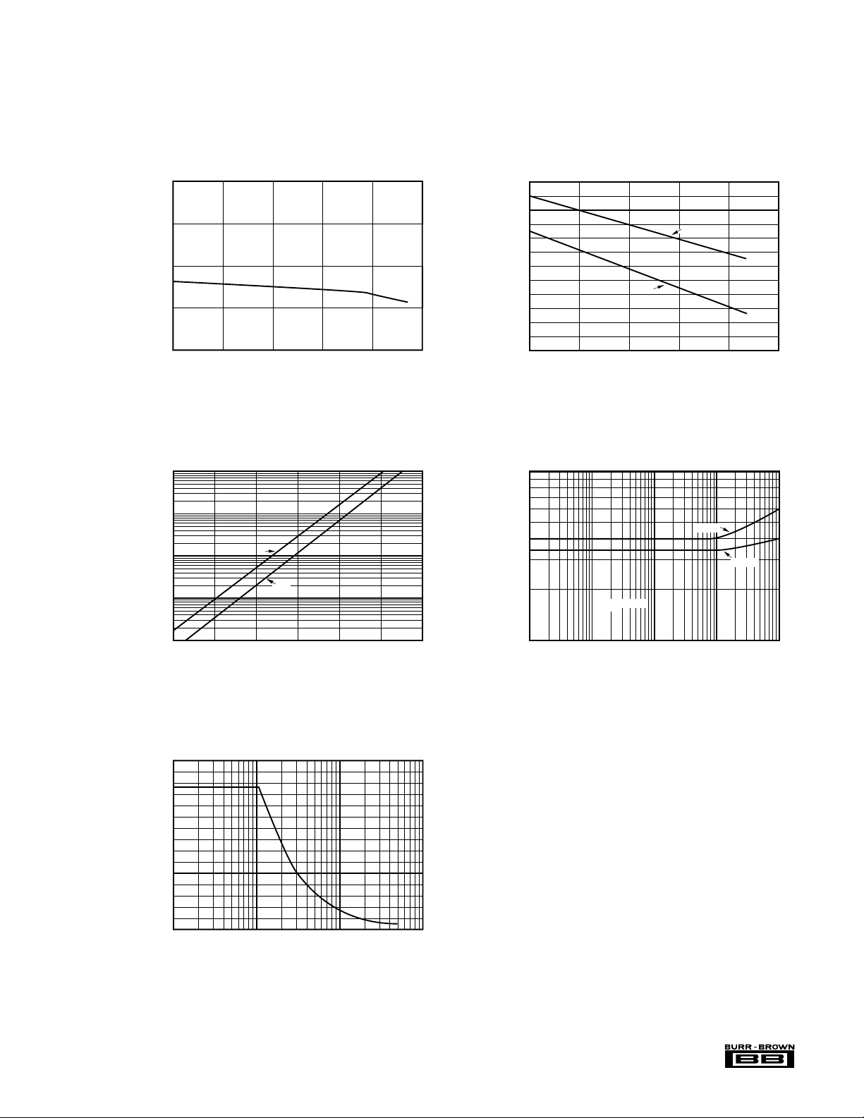
TYPICAL PERFORMANCE CURVES (CONT)
TOTAL HARMONIC DISTORTION + NOISE
vs FREQUENCY
Frequency (Hz)
10
100
1k
10k 100k
0.001
THD + N (%)
0.0001
0.0004
G = 1
G = 10
RL = 200Ω
TA = +25°C, VS = ±15V unless otherwise noted.
16.0
15.5
15.0
14.5
Power Supply Current (mA)
14.0
1000
100
POWER SUPPLY CURRENT vs TEMPERATURE
–25
INPUT BIAS CURRENT AND INPUT OFFSET CURRENT
10
0
25
Temperature (°C)
vs JUNCTION TEMPERATURE
I
B
50
75 100
SHORT-CIRCUIT CURRENT
120
110
100
90
80
Short-Circuit Current (mA)
70
60
–25
0
vs TEMPERATURE
I
–
I
SC
25
Temperature (°C)
50
+
SC
75 100
1
Input Bias And Offset Current (pA)
0
–25
MAX OUTPUT VOLTAGE SWING vs FREQUENCY
30
20
10
Max Output Voltage Swing (Vp-p)
0
100k
25
0
Junction Temperature (°C)
1M
I
OS
50
Frequency (Hz)
75
10M
100 125
100M
®
5
OPA671
Page 6
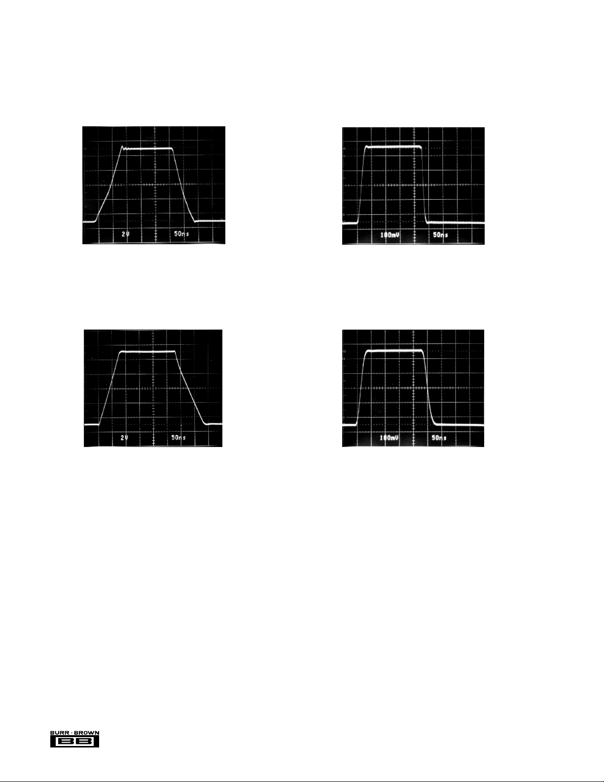
TYPICAL PERFORMANCE CURVES (CONT)
TA = +25°C, VS = ±15V unless otherwise noted.
G = +1 LARGE SIGNAL RESPONSE
G = +1 SMALL SIGNAL RESPONSE
G = –1 SMALL SIGNAL RESPONSEG = –1 LARGE SIGNAL RESPONSE
®
OPA671
6
Page 7
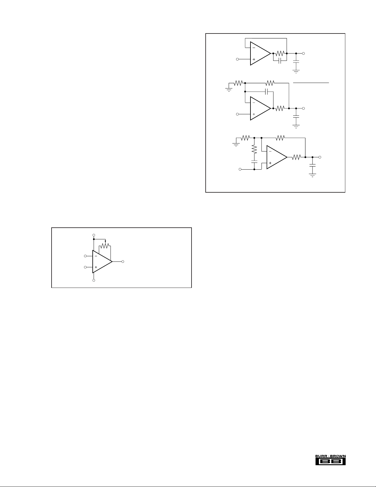
CIRCUIT LAYOUT
47kΩ
V
O
C
L
100pF
C
L
100pF
1000pF
C
C
10pF
47pF
R
C
20Ω
20Ω
250pF
G = 1
V
I
V
O
C
L
G = –1
V
I
1kΩ1kΩ
C
C
R
C
V
O
CL ≤ 100pF
V
I
1kΩ1kΩ
R
C
330Ω
100pF
(c)
(b)
(a)
G = –1
See application bulletin AB-028 for
details on circuits for driving capacitive loads.
With any high-speed, wide-bandwidth circuitry, careful circuit
layout will ensure best performance. Make short, direct circuit
interconnections and avoid stray wiring capacitance—especially at the inverting input pin. A component-side ground plane
will help ensure low ground impedance. Do not place the
ground plane under or near the inputs and feedback network.
The power supply connections should be bypassed with good
high-frequency capacitors positioned close to the op amp pins.
In most cases, both a 1µF solid tantalum capacitor and a 0.1µF
ceramic capacitor are required on each supply. The OPA671
can deliver peak load currents up to 100mA. Even if steadystate load currents are lower, signal transients may demand
large current transients from the power supplies. It is the power
supply bypass capacitors which must supply these current
transients. Larger bypass capacitors such as 4.7µF solid tantalum capacitors may improve dynamic performance in some
applications.
OFFSET ADJUSTMENT
Many applications require no external offset voltage adjustment. Figure 1 shows an optional circuit for trimming the offset
voltage. Do not use this offset voltage adjustment to correct for
offsets produced in other circuitry since this can introduce large
offset voltage temperature drift.
V+
10kΩ
7
1
2
5
OPA671
3
4
V–
FIGURE 1. Optional Offset Voltage Trim Circuit.
6
5kΩ to 50kΩ
Potentiometer
(10kΩ preferred)
FIGURE 2. Compensation Circuits for Capacitive Loads.
assure that the maximum junction temperature is not exceeded.
The OPA671 may be operated at reduced power supply voltage
to minimize power dissipation.
OUTPUT CURRENT LIMIT
Output current is limited by internal circuitry to approximately
90mA at 25°C. The short-circuit limit current decreases with
increasing junction temperature as shown in the typical curves.
The current limit will protect the device from inadvertent shortcircuits to ground. The internal power dissipation under this
condition, however, is quite high so short-circuits should be
avoided.
CAPACITIVE LOADS
The OPA671 is internally compensated to be unity-gain stable
with minimal capacitive load. The combination of low closedloop gain and capacitive load will decrease the phase margin
and may lead to gain peaking or oscillations. Load capacitance
reacts with the op amp’s open-loop output resistance to form an
additional pole in the feedback loop. With wideband op amps,
load capacitance as low as 50pF can introduce enough phase
shift to degrade dynamic performance. Figure 2 shows circuits
which preserve phase margin with capacitive load. Request
Application Bulletin AB-028 for details on various compensation circuits and analysis techniques.
POWER DISSIPATION
High output current can cause large internal power dissipation
in the OPA671. Copper leadframe construction improves heat
dissipation compared to conventional plastic packages. To
achieve best heat dissipation, solder the device directly to the
circuit board and use wide circuit board traces close to the
device pins. Limit the ambient temperature, load and signal to
INPUT BIAS CURRENT
The OPA671 is fabricated with Burr-Brown’s dielectrically
isolated
Difet
process, giving it extremely low input bias
current. As with other FET-input amplifiers, input bias current
approximately doubles with every 10°C increase in junction
temperature. Input bias current can be minimized by soldering
the device to the circuit board to provided best heat dissipation.
Reduced power supply voltage will also minimize input bias
current by reducing internal power dissipation.
DEMONSTRATION BOARD
The OPA671 may be evaluated using a high frequency PC
board developed for the OPA65x op amp family. This board
may be ordered from your local Burr-Brown distribution as part
# DEM-OPA65xP. It comes partially assembled but does not
include the amplifier. Since this board was intended for ±5V
amplifier, verify that any electrolytic capacitors loaded on the
board can support the higher supply voltages possible with the
OPA671.
7
OPA671
®
 Loading...