

Page 1
DESCRIPTION
The OPA651 is a low power, wideband voltage feedback operational amplifier. It features a bandwidth at
G = +2 of 470MHz as well as a 12-bit settling time of
only 16ns. The wide bandwidth and true differential
input stage make it suitable for use in a variety of
applications. Its low distortion gives exceptional performance for telecommunications, medical imaging
and video applications.
The OPA651 is compensated for stability in gains of
two or more, differentiating it from the unity gain
stable OPA650. Its unusual combination of speed,
accuracy and low power make it an outstanding choice
for many portable, multi-channel and other high speed
applications, where power is at a premium.
Wideband, Low Power Voltage Feedback
OPERATIONAL AMPLIFIER
© 1994 Burr-Brown Corporation PDS-1265E Printed in U.S.A. March, 1998
OPA651
®
FEATURES
● STABLE IN GAINS: ≥ 2V/V
● LOW POWER: 50mW
● BANDWIDTH: 470MHz at G = 2
● FAST SETTLING TIME: 16ns to 0.01%
● LOW HARMONICS: –78dB at 5MHz
● LOW INPUT BIAS CURRENT: 4
µA
● DIFFERENTIAL GAIN/PHASE ERROR:
0.01%/0.025
°
● LOW VOLTAGE NOISE: 4.6nV/√Hz
APPLICATIONS
● HIGH RESOLUTION VIDEO
● MONITOR PREAMPLIFIER
● CCD IMAGING AMPLIFIER
● ULTRASOUND SIGNAL PROCESSING
● ADC/DAC GAIN AMPLIFIER
● BASEBAND SIGNAL PROCESSING
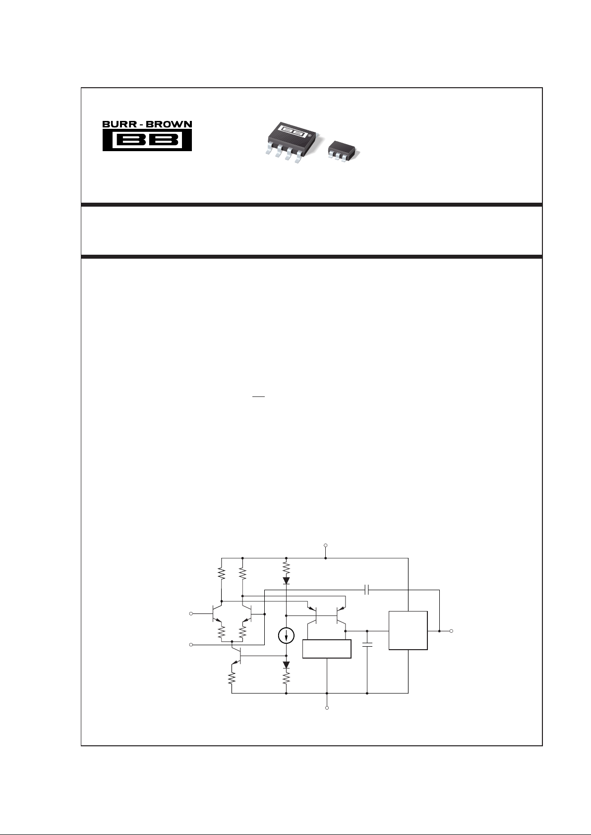
Current
Mirror
Output
Stage
C
C
Inverting
Input
Non-Inverting
Input
+V
S
Output
–V
S
1.5pF
International Airport Industrial Park • Mailing Address: PO Box 11400, Tucson, AZ 85734 • Street Address: 6730 S. Tucson Blvd., Tucson, AZ 85706 • Tel: (520) 746-1111 • Twx: 910-952-1111
Internet: http://www.burr-brown.com/ • FAXLine: (800) 548-6133 (US/Canada Only) • Cable: BBRCORP • Telex: 066-6491 • FAX: (520) 889-1510 • Immediate Product Info: (800) 548-6132
OPA651
Page 2
2OPA651
®
SPECIFICATIONS
At TA = +25°C, VS = ±5V, RL = 100Ω, RFB = 402Ω, G = +2, unless otherwise noted.
OPA651U, N OPA651UB, NB
PARAMETER CONDITIONS MIN TYP MAX MIN TYP MAX UNITS
FREQUENCY RESPONSE
Closed-Loop Bandwidth
(2)
G = +2 470 *
(1)
MHz
G = +5 70 * MHz
G = +10 34 * MHz
Gain Bandwidth Product 340 * MHz
Slew Rate G = +2, V
O
= 2V step 300 * V/µs
Over Specified Temperature 275 * V/µs
Rise Time 0.2V Step 0.8 * ns
Fall Time 0.2V Step 0.8 * ns
Settling Time 0.01% G = +2, V
O
= 2V step 16.2 * ns
0.1% G = +2, V
O
= 2V step 11.5 * ns
1% G = +2, V
O
= 2V step 7.2 * ns
Spurious Free Dynamic Range G = +2, f = 5.0 MHz, V
O
= 2Vp-p,
R
L
= 100Ω 67 * dBc
R
L
= 400Ω 78 * dBc
Differential Gain G = +2, NTSC, V
O
= 1.4Vp, RL = 150Ω 0.01 * %
Differential Phase G = +2, NTSC, V
O
= 1.4Vp, RL = 150Ω 0.025 * Degrees
Bandwidth For 0.1dB Flatness G = +2 43 * MHz
INPUT OFFSET VOLTAGE
Input Offset Voltage ±1 ±5.0 * ±2.0 mV
Average Drift ±3*µV/°C
Power Supply Rejection (+V
S
)V
S
= ±4.5V to ±5.5V 65 85 70 * dB
(–V
S
)526055*dB
INPUT BIAS CURRENT
Input Bias Current V
CM
= 0V 4 20 * 10 µA
Over Temperature 630 *20 µA
Input Offset Current V
CM
= 0V 0.4 1.5 * * µA
Over Temperature 0.9 3.0 * * µA
INPUT NOISE
Input Voltage Noise
Noise Density, f = 100Hz 13 * nV/√Hz
f = 10kHz 4.6 * nV/√Hz
f = 1MHz 4.6 * nV/√Hz
Voltage Noise, BW = 10Hz to 100MHz 46 * µVrms
Input Bias Current Noise
Current Noise Density, f = 0.1Hz to 20kHz 1.1 * pA/√Hz
Noise Figure (NF) R
S
= 10kΩ 3.2 * dB
R
S
= 50Ω 14 * dB
INPUT VOLTAGE RANGE
Common-Mode Input Range ±3.5 * V
Over Specified Temperature ±3.0 * V
Common-Mode Rejection V
CM
= ±0.5V 75 90 80 * dB
INPUT IMPEDANCE
Differential 60 || 1 * kΩ || pF
Common-Mode 2.6 || 1 * MΩ || pF
OPEN-LOOP GAIN
Open-Loop Voltage Gain V
O
= ±2V, RL = 100Ω 42 50 45 * dB
Over Specified Temperature V
O
= ±2V, RL = 100Ω 40 42 dB
OUTPUT
Voltage Output
Over Specified Temperature No Load ±2.2 ±3.0 ±2.4 * V
R
L
= 250Ω±2.2 ±2.5 ±2.4 * V
R
L
= 100Ω±2.0 ±2.3 ±2.1 * V
Current Output, Sourcing 75 110 * * mA
Over Specified Temperature 65 * mA
Current Output, Sinking 65 85 * * mA
Over Specified Temperature 35 * mA
Short Circuit Current 150 * mA
Output Resistance 0.1MHz, G = +2 0.05 * Ω
POWER SUPPLY
Specified Operating Voltage ±5*V
Operating Voltage Range ±4.5 ±5.5 * * V
Quiescent Current ±5.1 ±7.75 * ±6.5 mA
Over Specified Temperature ±8.75 ±7.5 mA
TEMPERATURE RANGE
Specification: U, N, UB, NB –40 +85 * * °C
Thermal Resistance,
θ
JA
U SO-8 125 * °C/W
N SOT23-5 150 * °C/W
NOTES: (1) An asterisk (*) specifies the same value as the grade to the left. (2) Frequency response can be strongly influenced by PC board parasitics. The OPA651
is nominally compensated assuming 2pF parasitic load. The demonstration boards show low parasitic layouts for the different package styles.
Page 3
3 OPA651
®
1
2
3
54+V
S
–Input
Output
–V
S
+Input
1
2
3
4
8
7
6
5
NC
+V
S
Output
NC
NC
–Input
+Input
–V
S
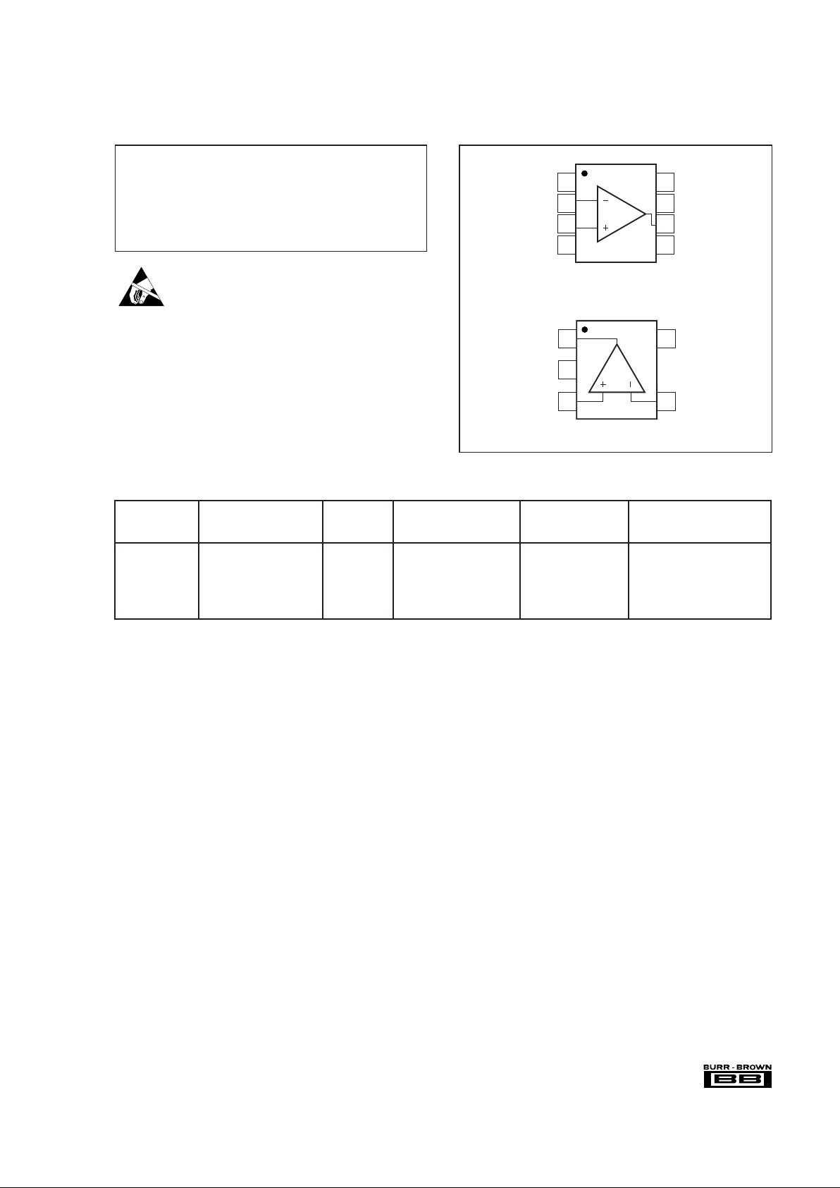
PIN CONFIGURATION
Top View SO-8
Supply ...............................................................................................±5.5V
Internal Power Dissipation
(1)
: .............................. See Thermal Conditions
Differential Input Voltage .................................................................. ±1.2V
Input Voltage Range ............................................................................ ±V
S
Storage Temperature Range: U, UB, N, NB ................ –40°C to +125°C
Lead Temperature (soldering, 10s) .............................................. +300°C
(soldering, SO-8 3s) ...................................................................... +260°C
Junction Temperature (T
J
) ............................................................ +175°C
ABSOLUTE MAXIMUM RATINGS
SOT23-5
ELECTROSTATIC
DISCHARGE SENSITIVITY
Electrostatic discharge can cause damage ranging from performance degradation to complete device failure. Burr-Brown
Corporation recommends that all integrated circuits be handled
and stored using appropriate ESD protection methods.
ESD damage can range from subtle performance degradation
to complete device failure. Precision integrated circuits may
be more susceptible to damage because very small parametric
changes could cause the device not to meet published specifications.
PACKAGE
DRAWING TEMPERATURE PACKAGE ORDERING
PRODUCT PACKAGE NUMBER
(1)
RANGE MARKING
(2)
NUMBER
(3)
OPA651U SO-8 Surface Mount 182 –40°C to +85°C OPA651U OPA651U
OPA651UB SO-8 Surface Mount 182 –40°C to +85°C OPA651UB OPA651UB
OPA651N 5-pin SOT23-5 331 –40°C to +85°C A51 OPA651N-250
OPA651N-3k
OPA651NB 5-pin SOT23-5 331 –40°C to +85°C A51B OPA651NB-250
OPA651NB-3k
NOTE: (1) For detailed drawing and dimension table, please see end of data sheet, or Appendix C of Burr-Brown IC Data Book. (2) The “B” grade of the SO-8 package
will be marked with a “B” by pin 8. The “B” grade of the SOT23-5 will be marked with a “B” near pins 3 and 4. (3) The SOT23-5 is only available on a 7" tape and reel
(e.g. ordering 250 pieces of “OPA651N-250” will get a single 250 piece tape and reel. Ordering 3000 pieces of “OPA651N-3k” will get a single 3000 piece tape and reel).
Please refer to Appendix B of Burr-Brown IC Data Book for detailed Tape and Reel Mechanical information.
PACKAGE/ORDERING INFORMATION
The information provided herein is believed to be reliable; however, BURR-BROWN assumes no responsibility for inaccuracies or omissions. BURR-BROWN assumes
no responsibility for the use of this information, and all use of such information shall be entirely at the user’s own risk. Prices and specifications are subject to change
without notice. No patent rights or licenses to any of the circuits described herein are implied or granted to any third party. BURR-BROWN does not authorize or warrant
any BURR-BROWN product for use in life support devices and/or systems.
Page 4
4OPA651
®
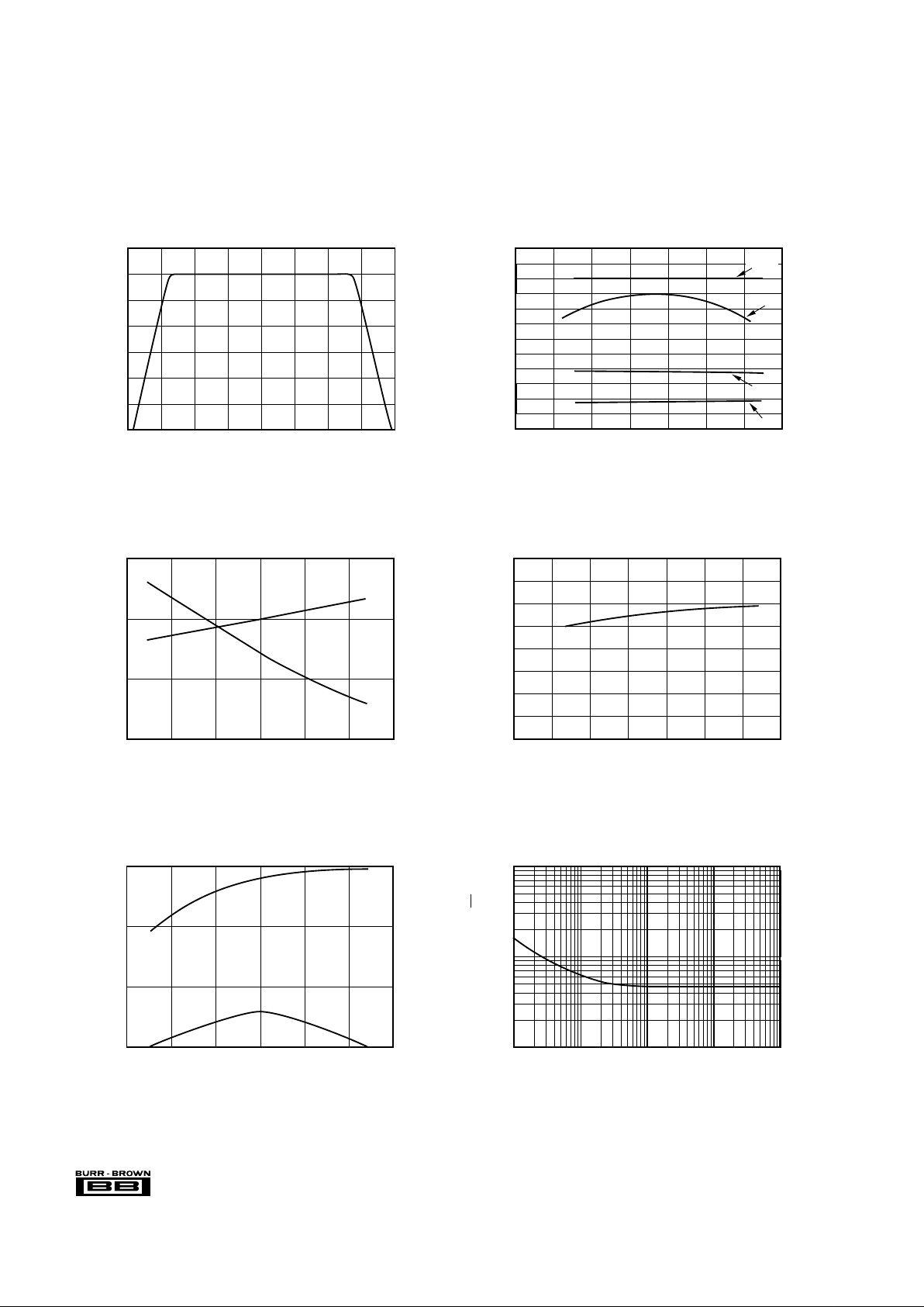
TYPICAL PERFORMANCE CURVES
At TA = +25°C, VS = ±5V, RL = 100Ω, RFB = 402Ω, and G = +2, unless otherwise noted.
OUTPUT CURRENT vs TEMPERATURE
110
100
90
80
–50 –25 0 25 50 75 100
Output Current (±mA)
Temperature (°C)
I
O
+
I
O
–
INPUT VOLTAGE NOISE DENSITY vs FREQUENCY
100 1k 10k 100k 1M
Input Voltage Noise (nV/√Hz)
Frequency (Hz)
100
10
1
SUPPLY CURRENT vs TEMPERATURE
8
7
6
5
4
3
2
1
0
–75 –50 –25 0 25 50 75 100
Supply Current (±mA)
Ambient Temperature (°C)
INPUT BIAS CURRENT AND OFFSET VOLTAGE
vs TEMPERATURE
7
6
5
4
2
1
0
–1
–50 –25 0 25 50 75 100
Input Bias Current (mA)
Offset Voltage (mV)
Temperature (°C)
V
OS
I
B
COMMON-MODE REJECTION RATIO
vs COMMON-MODE INPUT VOLTAGE
100
90
80
70
60
50
40
30
–4 –2–3 –101234
Common-Mode Rejection (dB)
Common-Mode Voltage (V)
AOL, PSR+, PSR–, AND CMRR vs TEMPERATURE
100
95
90
85
80
75
70
65
60
55
50
45
40
–75 –50 –25 0 25 50 75 100
A
OL
, PSR+, PSR–, and CMRR (dB)
Ambient Temperature (°C)
A
OL
PSR+
PSR–
CMRR
Page 5

5 OPA651
®
TYPICAL PERFORMANCE CURVES (CONT)
At TA = +25°C, VS = ±5V, RL = 100Ω, RFB = 402Ω, and G = +2, unless otherwise noted.
SMALL SIGNAL BANDWIDTH
G = +10 CLOSED-LOOP
100M
Frequency (Hz)
1M0 10M 1G
23
20
17
14
11
8
5
Gain (dB)
Bandwidth
= 34MHz
LARGE SIGNAL TRANSIENT RESPONSE
(G = +2)
Time (5ns/div)
2.0
1.6
1.2
0.8
0.4
0
–0.4
–0.8
–1.2
–1.6
–2.0
Output Voltage (V)
SMALL SIGNAL TRANSIENT RESPONSE
(G = +2)
Time (5ns/div)
160
120
80
40
0
–40
–80
–120
–160
Output Voltage (mV)
RECOMMENDED ISOLATION RESISTANCE
vs CAPACITIVE LOAD
40
30
20
10
0
0 20 40 60 80 100
Isolation Resistance, R
ISO
(Ω)
Capacitive Load, CL (pF)
R
ISO
OPA651
C
L
1kΩ
402Ω
402Ω
SMALL SIGNAL BANDWIDTH
G = +2 CLOSED-LOOP
100M
Frequency (Hz)
1M0 10M 1G
12
9
6
3
0
–3
Gain (dB)
SO-8 Bandwidth
= 472MHz
SMALL SIGNAL BANDWIDTH
G = +5 CLOSED-LOOP
100M
Frequency (Hz)
1M0 10M 1G
20
17
14
11
8
5
2
Gain (dB)
SO-8 Bandwidth
= 66MHz
Page 6

6OPA651
®
TYPICAL PERFORMANCE CURVES (CONT)
At TA = +25°C, VS = ±5V, RL = 100Ω, RFB = 402Ω, and G = +2, unless otherwise noted.
HARMONIC DISTORTION vs GAIN
(f = 5MHz, V
O
= 2V
p–p
)
Non-Inverting Gain (V/V)
12345678910
–40
–50
–60
–70
–80
Harmonic Distortion (dBc)
3fo
2fo
10MHz HARMONIC DISTORTION vs OUTPUT SWING
(G = +2)
Output Swing (V
p–p
)
01234
–50
–55
–60
–65
–70
–75
–80
–85
–90
Harmonic Distortion (dBc)
3fo
2fo
5MHz HARMONIC DISTORTION vs OUTPUT SWING
(G = +2)
Output Swing (V
p–p
)
01234
–55
–60
–65
–70
–75
–80
–85
–90
–95
Harmonic Distortion (dBc)
3fo
2fo
HARMONIC DISTORTION vs TEMPERATURE
(f = 5MHz, V
O
= 2V
p-p
, G = +2)
–55
–60
–65
–70
–75
–75 –50 –25 0 25 50 75 100
Harmonic Distortion (dBc)
Ambient Temperature (°C)
3fo
2fo
HARMONIC DISTORTION vs FREQUENCY
(G = +2, V
O
= 2V
p–p, RL
= 100Ω)
10M
Frequency (Hz)
100k 1M 100M
–40
–45
–50
–55
–60
–65
–70
–75
–80
–85
–90
Harmonic Distortion (dBc)
3fo
2fo
OPEN-LOOP GAIN AND PHASE vs FREQUENCY
60
40
20
0
–20
–40
0
–45
–90
–135
–180
–225
1k 10k 100k 1M 10M 100M 1G
Gain (dB)
Phase (°)
Frequency (Hz)
Gain
Phase
Page 7

7 OPA651
®
DISCUSSION OF
PERFORMANCE
The OPA651 is a low power, wideband voltage feedback
operational amplifier, internally compensated to provide gain
of +2 stability. The OPA651’s voltage feedback architecture
features true differential and fully symmetrical inputs. This
minimizes offset errors, making the OPA651 well suited for
implementing filter and instrumentation designs. The
OPA651’s AC performance is optimized to provide a gain
bandwidth product of 340MHz and a fast 0.1% settling time
of 11.5ns, which is an important consideration in high speed
data conversion applications. Along with its excellent settling
characteristics, the low DC input offset of ±1mV and drift of
±3µV/°C support high accuracy requirements. In applications requiring a higher slew rate and wider bandwidth, such
as video and high bit rate digital communications, consider
the current feedback OPA658.
CIRCUIT LAYOUT AND BASIC OPERATION
Achieving optimum performance with a high frequency amplifier like the OPA651 requires careful attention to layout
parasitics and selection of external components. Recommendations for PC board layout and component selection include:
a) Minimize parasitic capacitance to any ac ground for all
of the signal I/O pins. Parasitic capacitance on the output
and inverting input pins can cause instability; on the noninverting input it can react with the source impedance to
cause unintentional bandlimiting. To reduce unwanted capacitance, a window around the signal I/O pins should be
opened in all of the ground and power planes. Otherwise,
ground and power planes should be unbroken elsewhere on
the board.
b) Minimize the distance (< 0.25") from the two power pins
to high frequency 0.1µF decoupling capacitors. At the pins,
the ground and power plane layout should not be in close
proximity to the signal I/O pins. Avoid narrow power and
ground traces to minimize inductance between the pins and
the decoupling capacitors. Larger (2.2µF to 6.8µF) decoupling
capacitors, effective at lower frequencies, should also be
used. These may be placed somewhat farther from the
device and may be shared among several devices in the same
area of the PC board.
c) Careful selection and placement of external components will preserve the high frequency performance of the
OPA651. Resistors should be a very low reactance type.
Surface mount resistors work best and allow a tighter overall
layout. Metal film or carbon composition axially-leaded
resistors can also provide good high frequency performance.
Again, keep their leads as short as possible. Never use
wirewound type resistors in a high frequency application.
Since the output pin and the inverting input pin are most
sensitive to parasitic capacitance, always position the feedback and series output resistor, if any, as close as possible to
the package pins. Other network components, such as noninverting input termination resistors, should also be placed
close to the package.
Even with a low parasitic capacitance shunting external
resistors, excessively high resistor values can create significant time constants and degrade performance. This is particularly true for the OPA651 with its internal 1.5pF feedback capacitance. Good metal film or surface mount resistors have approximately 0.2pF in shunt with the resistor. For
resistor values > 1.5kΩ, this adds a pole and/or zero below
500MHz that can affect circuit operation. Keep resistor
values as low as possible consistent with output loading
considerations. The 402Ω feedback used for the Typical
Performance Plots is a good starting point for design.
d) Connections to other wideband devices on the board
may be made with short direct traces or through on-board
transmission lines. For short connections, consider the trace
and the input to the next device as a lumped capacitive load.
Relatively wide traces (50 to 100 mils) should be used,
preferably with ground and power planes opened up around
them. Estimate the total capacitive load and set R
ISO
from
the plot of recommended R
ISO
vs capacitive load. Low
parasitic loads may not need an R
ISO
since the OPA651 is
nominally compensated to operate with a 2pF parasitic load.
If a long trace is required and the 6dB signal loss intrinsic to
doubly terminated transmission lines is acceptable, implement a matched impedance transmission line using microstrip
or stripline techniques (consult an ECL design handbook for
microstrip and stripline layout techniques). A 50Ω environment is not necessary on board, and in fact a higher impedance environment will improve distortion as shown in the
distortion vs load plot. With a characteristic impedance
defined based on board material and desired trace dimensions, a matching series resistor into the trace from the
output of the amplifier is used as well as a terminating shunt
resistor at the input of the destination device. Remember
also that the terminating impedance will be the parallel
combination of the shunt resistor and the input impedance of
the destination device; the total effective impedance should
match the trace impedance. Multiple destination devices are
best handled as separate transmission lines, each with their
own series and shunt terminations.
If the 6dB attenuation loss of a doubly terminated line is
unacceptable, a long trace can be series-terminated at the
source end only. This will help isolate the line capacitance
from the op amp output, but will not preserve signal integrity
as well as a doubly terminated line. If the shunt impedance
at the destination end is finite, there will be some signal
attenuation due to the voltage divider formed by the series
and shunt impedances.
The OPA651 is nominally specified for operation using ±5V
power supplies. A 10% tolerance on the supplies, or an ECL
–5.2V for the negative supply, is within the maximum specified total supply voltage of 11V. Higher supply voltages can
break down internal junctions possibly leading to catastrophic
failure. Single supply operation is possible as long as common mode voltage constraints are observed. The common
Page 8

8OPA651
®
mode input and output voltage specifications can be interpreted as a required headroom to the supply voltage. Observing this input and output headroom requirement will allow
non-standard or single supply operation. Figure 1 shows one
approach to single-supply operation.
ESD PROTECTION
ESD damage has been well recognized for MOSFET devices, but any semiconductor device is vulnerable to this
potentially damaging source. This is particularly true for
very high speed, fine geometry processes.
ESD damage can cause subtle changes in amplifier input
characteristics without necessarily destroying the device. In
precision operational amplifiers, this may cause a noticeable
degradation of offset voltage and drift. Therefore, ESD
handling precautions are strongly recommended when handling the OPA651.
OUTPUT DRIVE CAPABILITY
The OPA651 has been optimized to drive 75Ω and 100Ω
resistive loads. The device can drive a 2Vp-p into a 75Ω load.
This high-output drive capability makes the OPA651 an ideal
choice for a wide range of RF, IF, and video applications. In
many cases, additional buffer amplifiers are unneeded.
Many demanding high-speed applications such as driving
A/D converters require op amps with low wideband output
impedance. For example, low output impedance is essential
when driving the signal-dependent capacitances at the inputs
of flash A/D converters. As shown in Figure 3, the OPA651
maintains very low-closed loop output impedance over frequency. Closed-loop output impedance increases with frequency since loop gain is decreasing.
402Ω
OPA651
V
AC
402Ω
R
L
+V
S
+V
S
V
S
2
R
OUT
V
S
2
V
OUT
= + 2•V
AC
THERMAL CONSIDERATIONS
The OPA651 will not require heatsinking under most operating conditions. Maximum desired junction temperature
will limit the maximum allowed internal power dissipation
as described below. In no case should the maximum junction
temperature be allowed to exceed +175°C.
FIGURE 3. Small-Signal Output Impedance vs Frequency.
SMALL-SIGNAL OUTPUT IMPEDANCE
vs FREQUENCY
Frequency (Hz)
1k
100
10
1
0.1
0.01
10k 100k 1M 100M10M
Output Impedance (Ω)
G = +2
OFFSET VOLTAGE ADJUSTMENT
If additional offset adjustment is needed, the circuit in
Figure 2 can be used without degrading offset drift with
temperature. Avoid external adjustment whenever possible
since extraneous noise, such as power supply noise, can be
inadvertently coupled into the amplifier’s inverting input
terminal. Remember that additional offset errors can be
created by the amplifier’s input bias currents. Whenever
possible, match the impedance seen by both inputs as is
shown with R
3
. This will reduce input bias current errors to
the amplifier’s offset current.
R
2
OPA651
(1)
R3 = R1 || R
2
R
1
R
Trim
+V
S
–V
S
20kΩ
VIN or Ground
Output Trim Range +V
S
to –V
S
≅
R
Trim
47kΩ
R
2
R
2
R
Trim
0.1µF
NOTE: (1) R3 is
optional and can
be used to cancel
offset errors due
to input bias currents.
FIGURE 2. Offset Voltage Trim.
FIGURE 1. Single Supply Operation.
Page 9

9 OPA651
®
Operating junction temperature (TJ) is given by TA +
P
DθJA
. The total internal power dissipation (PD) is a com-
bination of the total quiescent power (P
DQ
) and the power
dissipated in of the output stage (P
DL
) to deliver load
power. Quiescent power is simply the specified no-load
supply current times the total supply voltage across the
part. P
DL
will depend on the required output signal and load
but would, for a grounded resistive load, be at a maximum
when the output is a fixed DC voltage equal to 1/2 of either
supply voltage (assuming equal bipolar supplies). Under
this condition, PDL = V
S
2
/(4•RL) where RL includes feedback network loading. Note that it is the power dissipated
in the output stage and not in the load that determines
internal power dissipation. As an example, compute the
maximum TJ for an OPA651N at AV = +2, RL = 100Ω, R
FB
= 402Ω, ±VS = ±5V, with the output at |VS/2|, and the
specified maximum T
A
= +85°C. PD = 10V•8.75mA + (52)/
(4•(100Ω||804Ω)) = 158mW. Maximum T
J
= +85°C +
0.158W•150°C/W = 109°C.
DRIVING CAPACITIVE LOADS
The OPA651’s output stage has been optimized to drive low
resistive loads. Capacitive loads, however, will decrease the
amplifier’s phase margin which may cause high frequency
peaking or oscillations. Capacitive loads greater than 10pF
should be isolated by connecting a small resistance, usually
15Ω to 30Ω, in series with the output as shown in Figure 4.
This is particularly important when driving high capacitance
loads such as flash A/D converters. Increasing the gain from
+2 will improve the capacitive load drive due to increased
phase margin.
In general, capacitive loads should be minimized for optimum high frequency performance. Coax lines can be driven
if the cable is properly terminated. The capacitance of coax
cable (29pF/foot for RG-58) will not load the amplifier
when the coaxial cable or transmission line is terminated in
its characteristic impedance.
that, from a stability standpoint, an inverting gain of –1V/V
is equivalent to a noise gain of 2.) Frequency response for
other gains are shown in the Typical Performance Curves.
The high frequency response of the OPA651 in a good
layout is very flat with frequency. However, some circuit
configurations such as those where large feedback resistances are used, can produce high-frequency gain peaking.
This peaking can be minimized by connecting a small
capacitor in parallel with the feedback resistor. This capacitor compensates for the closed-loop, high-frequency, transfer function zero that results from the time constant formed
by the input capacitance of the amplifier (typically 2pF after
PC board mounting), and the input and feedback resistors.
The selected compensation capacitor may be a trimmer, a
fixed capacitor, or a planned PC board capacitance. The
capacitance value is strongly dependent on circuit layout and
closed-loop gain. Using small resistor values will preserve
the phase margin and avoid peaking by keeping the break
frequency of this zero sufficiently high. When high closedloop gains are required, a three-resistor attenuator (teenetwork) is recommended to avoid using large value resistors with large time constants. The OPA651 includes an
internal 1.5pF feedback capacitor to achieve best gain of +2
flatness (R
F
= 402Ω).
PULSE SETTLING TIME
High speed amplifiers like the OPA651 are capable of
extremely fast settling time with a pulse input. Excellent
frequency response flatness and phase linearity are required
to get the best settling times. As shown in the specifications
table, settling time for a ±1V step at a gain of +2 for the
OPA651 is extremely fast. The specification is defined as
the time required, after the input transition, for the output to
settle within a specified error band around its final value. For
a 2V step, 1% settling corresponds to an error band of
±20mV, 0.1% to an error band of ±2mV, and 0.01% to an
error band of ±0.2mV. For the best settling times, particularly into an ADC capacitive load, little or no peaking in the
frequency response can be allowed. Using the recommended
R
ISO
for capacitive loads will limit this peaking and reduce
the settling times. Fast, extremely fine scale settling (0.01%)
requires close attention to ground return currents in the
supply decoupling capacitors. For highest performance, consider the OPA642 which isolates the output stage decoupling
from the rest of the amplifier.
DIFFERENTIAL GAIN AND PHASE
Differential Gain (DG) and Differential Phase (DP) are
among the more important specifications for video applications. The percentage change in closed-loop gain over a
specified change in output voltage level is defined as DG.
DP is defined as the change in degrees of the closed-loop
phase over the same output voltage change. DG and DP are
both specified at the NTSC sub-carrier frequency of 3.58MHz.
All measurements were performed using an HP 9480.
FIGURE 4. Driving Capacitive Loads.
OPA651
C
L
R
L
R
ISO
(R
ISO
typically 15Ω to 30Ω)
402Ω402Ω
FREQUENCY RESPONSE COMPENSATION
The OPA651 is internally compensated and is stable at a
gain of 2 with a phase margin of approximately 60°. (Note
Page 10

10OPA651
®
DISTORTION
The OPA651’s harmonic distortion characteristics into a
100Ω load are shown versus frequency and power output in
the typical performance curves. Distortion can be significantly improved by increasing the load resistance as illustrated in Figure 5. Remember to include the contribution of
the feedback network when calculating the effective load
resistance seen by the amplifier.
10 100 1k
–50
–55
–60
–65
–70
–75
–80
Harmonic Distortion (dBc)
3fo
2fo
G = +2
Load Resistance (Ω)
FIGURE 5. 5MHz Harmonic Distortion vs Load Resistance.
NOISE FIGURE
The OPA651 voltage noise spectral density is specified in
the Typical Performance Curves. For RF applications, however, Noise Figure (NF) is often the preferred noise specification since it allows system noise performance to be more
easily calculated. The OPA651’s Noise Figure vs Source
Resistance is shown in Figure 6.
NOISE FIGURE vs SOURCE RESISTANCE
Source Resistance (Ω)
30
25
20
15
10
5
0
10 100 1k 100k10k
Noise Figure (dB)
NF = 10 LOG 1 +
e
n
2
+ (InRS)
2
4KTR
S
FIGURE 6. Noise Figure vs Source Resistance.
SPICE MODELS AND EVALUATION BOARD
Computer simulation of circuit performance using SPICE is
often useful when analyzing the performance of analog
circuits and systems. This is particularly true for Video and
RF amplifier circuits where parasitic capacitance and inductance can have a major effect on circuit performance. SPICE
models are available on a disk from the Burr-Brown Applications Department.
Demonstration boards are available for each OPA651 package style. These boards implement a very low parasitic
layout that will produce the excellent frequency and pulse
responses shown in the Typical Performance Curves. For
each package style, the recommended demonstration board
is:
Contact your local Burr-Brown sales office or distributor to
order demonstration boards.
BOARD LITERATURE
PART REQUEST
PRODUCT PACKAGE NUMBER NUMBER
OPA651P 8-Pin DIP DEM-OPA65xP —
OPA651U 8-Pin SO-8 DEM-OPA65xU —
OPA651N 6-Pin SOT23-6 DEM-OPA6xxN MKT-348
OPA651
V
OUT
402Ω402Ω
Video
Input
75Ω
75Ω
75Ω Transmission Line
75Ω
TYPICAL APPLICATION
FIGURE 7. Low Distortion Video Amplifier.
Page 11

11 OPA651
®
FIGURE 8. Layout Detail For DEM-OPA65xU Demonstration Board.
NOTE: Values for R1, R2, R3, R5, R6, R7 and R8 are chosen according to desired gain.
R
6
R
1
OPA651
Out
J
1
1
2
GND
–5V
P2
R
7
R
5
+In
R
3
R
4
R
2
–In
J
1
J
2
2
7
4
6
3
C
2
0.1µF
C
4
2.2µF
402Ω
C
1
2.2µF
C
3
0.1µF
1
2
GND
+5V
P1
R
8
+
+
 Loading...