

Datasheet OPA643N-250, OPA643NB-3K, OPA643U, OPA643UB, OPA643NB-250 Datasheet (Burr Brown)
...Page 1
®
OPA643
1
Wideband Low Distortion, High Gain
OPERATIONAL AMPLIFIER
®
OPA643
APPLICATIONS
● BASE STATION ADC PREAMP
● ADC/DAC BUFFER AMPLIFIER
● LOW DISTORTION IF AMPLIFIER
● LOW NOISE, BROADBAND,
TRANSIMPEDANCE AMPLIFIER
● LOW NOISE PREAMPLIFIER
● VIDEO AMPLIFICATION
● TEST INSTRUMENTATION
OPA643
OPA658
OPA643
International Airport Industrial Park • Mailing Address: PO Box 11400, Tucson, AZ 85734 • Street Address: 6730 S. Tucson Blvd., Tucson, AZ 85706 • Tel: (520) 746-1111 • Twx: 910-952-1111
Internet: http://www.burr-brown.com/ • FAXLine: (800) 548-6133 (US/Canada Only) • Cable: BBRCORP • Telex: 066-6491 • FAX: (520) 889-1510 • Immediate Product Info: (800) 548-6132
FEATURES
● LOW DISTORTION: –90dBc at 5MHz
● LOW NOISE: 2.3nV/√Hz
● GAIN-BANDWIDTH PRODUCT: 800MHz
● AVAILABLE IN SOT23-5 PACKAGE
● STABLE IN GAINS
≥ 3
● HIGH SLEW RATE: 1000V/
µs
● HIGH OPEN-LOOP GAIN: 95dB
● HIGH OUTPUT CURRENT:
±60mA
DESCRIPTION
The OPA643 provides a level of speed and dynamic
range previously unattainable in a monolithic op amp.
Using a de-compensated voltage feedback architecture with two internal gain stages, the OPA643 achieves
exceptionally low harmonic distortion over a wide
frequency range. The "classic" differential input provides all the familiar benefits of precision op amps,
such as bias current cancellation and very low inverting current noise compared with wideband current
feedback op amps. High slew rate and open-loop gain,
along with low input noise and high output current
drive make the OPA643 ideal for very high dynamic
range requirements.
The high gain bandwidth product for the gain ≥ 3
stable OPA643 makes it particularly suitable for
wideband transimpedance amplifiers and moderate gain
IF amplifier applications. External compensation
techniques may be used to apply the OPA643 at low
gains giving exceptionally low distortion and frequency
response flatness. Where unity gain stability with
comparable distortion performance is required, consider
the OPA642.
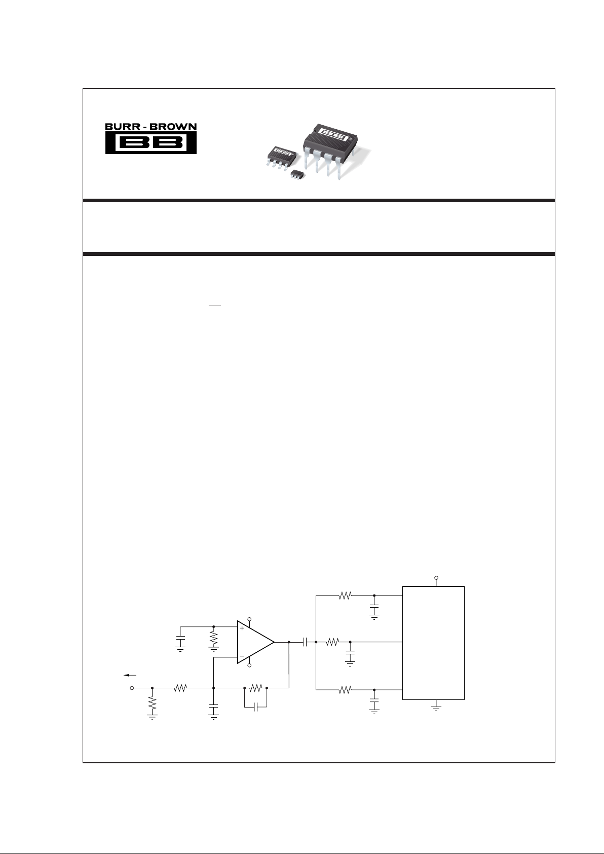
806Ω
50Ω
1Vp-p
10MHz
OPA643
47pF
REFT
+5V
REFB
ADS805
12-Bit
20MSPS
Measured
80dB SFDR
Analog
Input
56.9Ω
0.1µF
0.1µF
402Ω
5kΩ
High Dynamic Range 20MSPS Digitizer
5kΩ
0.1µF
2Vp-p
+5V
–5V
14pF
280Ω
0.1µFLow Gain
Compensation
50Ω
Source
2.7pF
©
1993 Burr-Brown Corporation PDS-1191D Printed in U.S.A. March, 1998
Page 2

®
OPA643
2
SPECIFICATIONS
ELECTRICAL
At TA = +25°C, VS = ±5V, RL = 100Ω, RF = 402Ω, unless otherwise noted.
OPA643P, U, N OPA643PB, UB, NB
PARAMETER CONDITIONS MIN TYP MAX MIN TYP MAX UNITS
OFFSET VOLTAGE
Input Offset Voltage ±2.5 ±4 ±0.5 ±1.5 mV
Average Drift 53µV/°C
Power Supply Rejection (PSR) V
S
= ±4.5 to ±5.5V 65 90 70 ✻ dB
INPUT BIAS CURRENT
Input Bias Current V
CM
= 0V 19 30 ✻✻ µA
Over Specified Temperature 40 ✻ µA
Input Offset Current V
CM
= 0V 0.1 2.0 ✻✻ µA
Over Specified Temperature 3.0 ✻ µA
NOISE
Input Voltage Noise
Noise Density: f > 1MHz 2.3 ✻ nV/√Hz
Integrated Voltage Noise, BW = 100Hz to 100MHz 23 ✻ µVrms
Input Bias Current Noise
Current Noise Density, f > 1MHz 2.5 ✻ pA/√Hz
INPUT VOLTAGE RANGE
Common-Mode Input Range ±2.75 ±3.0 ✻✻ V
Over Specified Temperature ±2.5 ✻ V
Common-Mode Rejection (CMR) V
CM
= ±0.5V 65 85 80 92 dB
INPUT IMPEDANCE
Differential 7 || 2.5 ✻ kΩ || pF
Common-Mode 630 || 1.3 ✻ kΩ || pF
OPEN-LOOP GAIN
Open-Loop Voltage Gain (A
OL
)V
O
= ±2V, RL = 100Ω 82 95 87 ✻ dB
Over Specified Temperature V
O
= ±2V, RL = 100Ω 80 80 dB
FREQUENCY RESPONSE
Closed-Loop Bandwidth Gain = +5V/V 200 ✻ MHz
Gain = +10V/V 85 ✻ MHz
Gain = +20V/V 40 ✻ MHz
Gain Bandwidth Product (GBP) 800 ✻ MHz
Slew Rate
(1)
G = +5, 2V Step 1000 ✻ V/µs
At Minimum Specified Temperature G = +5, 2V Step 920 ✻ V/µs
Settling Time: 0.01% G = +5, 2V Step 21 ✻ ns
0.1% G = +5, 2V Step 16.5 ✻ ns
1% G = +5, 2V Step 7.5 ns
Spurious Free Dynamic Range (SFDR) G = +5, f = 5MHz 90 95 dBc
V
O
= 2Vp-p, RL = 500Ω
Differential Gain Error at 3.58MHz G = +5V/V, V
O
= 0V to 1.4V, RL = 150Ω 0.005 ✻ %
Differential Phase Error at 3.58MHz G = +5V/V, V
O
= 0V to 1.4V, RL = 150Ω 0.015 ✻ degrees
OUTPUT
Voltage Output No Load ±3.25 ✻ V
Over Specified Temperature ±3.0 ✻ V
Voltage Output, +25°CR
L
= 100Ω±2.75 ✻ V
Over Specified Temperature ±2.5 ✻ V
Current Output, +25°C ±40 ±60 ±50 ±65 mA
Over Specified Temperature ±35 ±40 mA
Closed-Loop Output Resistance 0.1MHz, G = +5V/V 0.055 ✻ Ω
POWER SUPPLY
Specified Operating Voltage ±5 ✻ V
Operating Voltage Range T
MIN
to T
MAX
±4.5 ±5.5 ✻✻V
Quiescent Current ±20 ±25 ±16 ✻✻ mA
Over Specified Temperature ±26 ✻ mA
TEMPERATURE RANGE
Specification: P, U, N Ambient –40 +85 ✻✻°C
Thermal Resistance
θ
JA
, Junction to Ambient
P, PB 8-Pin DIP 100 ✻ °C/W
U, UB 8-Pin SO-8 125 ✻ °C/W
N, NB 5-Pin SOT23-5 150 ✻ °C/W
✻ Specifications same as OPA643P, U, N.
NOTE: (1) Slew rate is rate of change from 10% to 90% of output voltage step.
Page 3
®
OPA643
3
1
2
3
54+V
S
Inverting Input
Output
–V
S
Non-Inverting Input
1
2
3
4
8
7
6
5
+V
S2
(1)
+V
S1
Output
–V
S2
(1)
NC
Inverting Input
Non-Inverting Input
–V
S1
The information provided herein is believed to be reliable; however, BURR-BROWN assumes no responsibility for inaccuracies or omissions. BURR-BROWN assumes
no responsibility for the use of this information, and all use of such information shall be entirely at the user’s own risk. Prices and specifications are subject to change
without notice. No patent rights or licenses to any of the circuits described herein are implied or granted to any third party. BURR-BROWN does not authorize or warrant
any BURR-BROWN product for use in life support devices and/or systems.
PIN CONFIGURATION
Top View DIP/SO-8
ABSOLUTE MAXIMUM RATINGS
Power Supply (±VS)..................................................................... ±6.0VDC
Internal Power Dissipation
(1)
.................................. See Thermal Analysis
Differential Input Voltage .................................................................. ±1.2V
Input Voltage Range ............................................................................ ±V
S
Storage Temperature Range: P, PB, U, UB, N, NB ..... –40°C to +125°C
Lead Temperature (soldering, 10s).............................................. +300°C
(soldering, SO-8 3s) ....................................... +260°C
Junction Temperature (T
J
) ............................................................ +175°C
NOTE: (1) Packages must be derated based on specified
θ
JA. Maximum T
J
must be observed.
NOTE: (1) Making use of all four power supply pins is highly recommended,
although not required. Using these four pins, instead of just pins 4 and 7, will
lower the power supply impedance improving distortion.
SOT23-5
PACKAGE
DRAWING TEMPERATURE PACKAGE ORDERING
PRODUCT PACKAGE NUMBER
(1)
RANGE MARKING
(2)
NUMBER
(3)
OPA643U SO-8 Surface Mount 182 –40°C to +85°C OPA643U OPA643U
OPA643UB SO-8 Surface Mount 182 –40°C to +85°C OPA643UB OPA643UB
OPA643N 5-pin SOT23-5 331 –40°C to +85°C A43 OPA643N-250
OPA643N-3k
OPA643NB 5-pin SOT23-5 331 –40°C to +85°C A43B OPA643NB-250
OPA643NB-3k
OPA643P 8-Pin Plastic DIP 006 –40°C to +85°C OPA643P OPA643P
OPA643PB 8-Pin Plastic DIP 006 –40°C to +85°C OPA643PB OPA643PB
NOTES: (1) For detailed drawing and dimension table, please see end of data sheet, or Appendix C of Burr-Brown IC Data Book. (2) The “B” grade of the SO-8 and
DIP packages will be marked with a “B” by pin 8. The “B” grade of the SOT23-5 will be marked with a “B” near pins 3 and 4. (3) The SOT23-5 is only available on a 7"
tape and reel (e.g. ordering 250 pieces of “OPA643N-250” will get a single 250 piece tape and reel. Ordering 3000 pieces of “OPA643N-3k” will get a single 3000 piece
tape and reel). Please refer to Appendix B of Burr-Brown IC Data Book for detailed Tape and Reel Mechanical information.
PACKAGE/ORDERING INFORMATION
ELECTROSTATIC
DISCHARGE SENSITIVITY
Electrostatic discharge can cause damage ranging from performance degradation to complete device failure. Burr-Brown
Corporation recommends that all integrated circuits be handled
and stored using appropriate ESD protection methods.
ESD damage can range from subtle performance degradation
to complete device failure. Precision integrated circuits may
be more susceptible to damage because very small parametric
changes could cause the device not to meet published specifications.
Page 4
®
OPA643
4
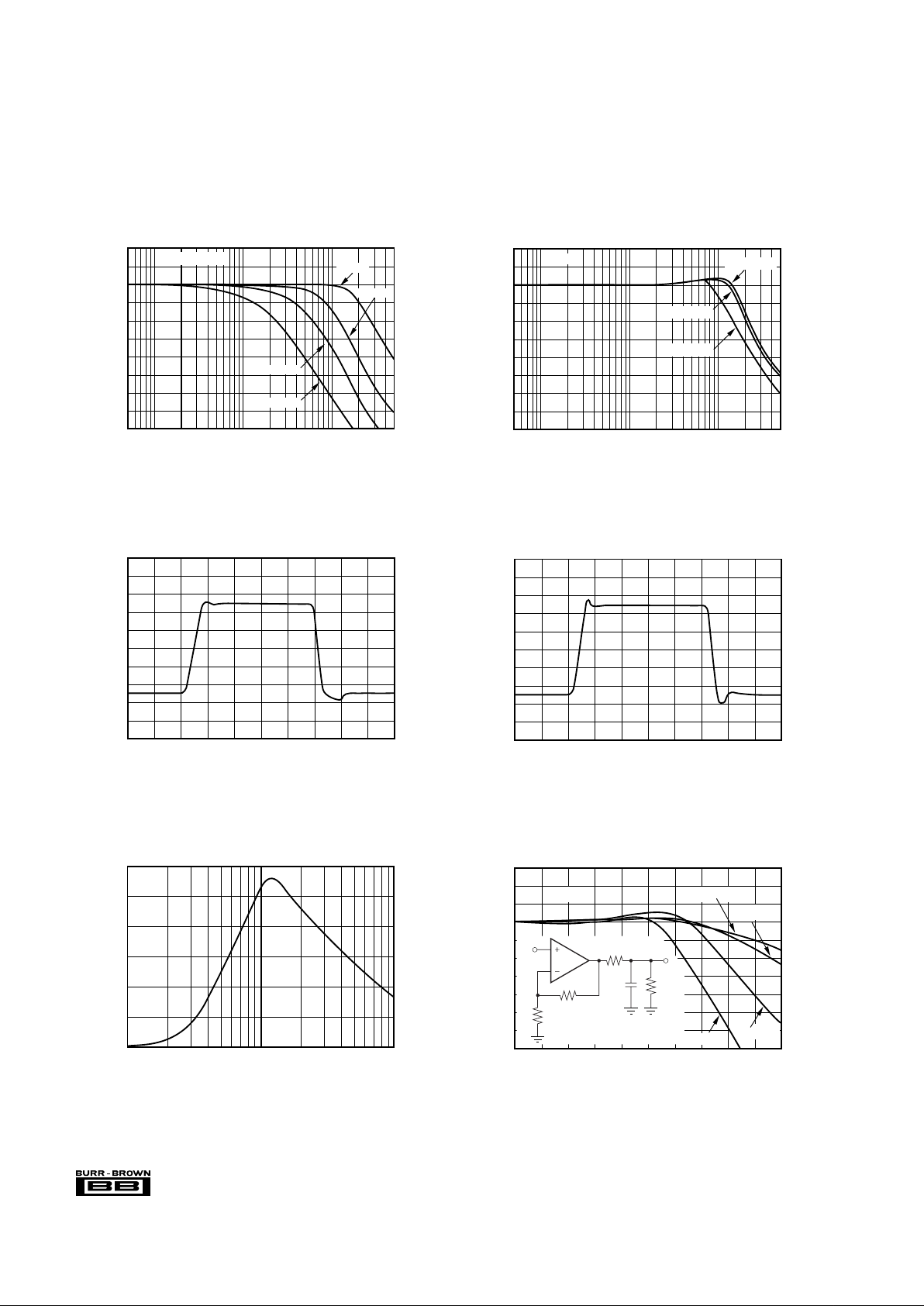
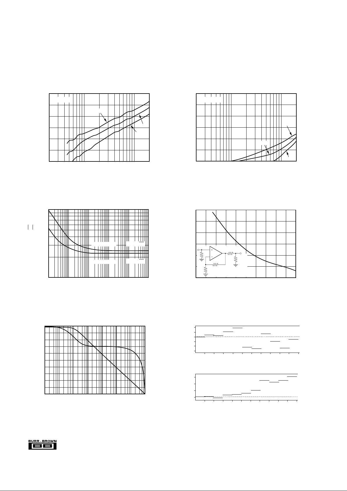
TYPICAL PERFORMANCE CURVES
At TA = +25°C, VS = ±5V, RL = 100Ω, RF = 402Ω, unless otherwise noted
LARGE SIGNAL FREQUENCY RESPONSE
Frequency
0.5MHz 10MHz 100MHz 500MHz
20
17
14
11
8
5
2
–1
–4
–7
–10
Gain (3dB/div)
G = +5
VO = 1Vp-p
VO = 2Vp-p
VO = 4Vp-p
RS vs CAPACITIVE LOAD
Capacitive Load (pF)
101 100
60
50
40
30
20
10
0
R
S
(Ω)
LARGE SIGNAL PULSE RESPONSE
Time (5ns/div)
2.0
1.6
1.2
0.8
0.4
0
–0.4
–0.8
–1.2
–1.4
–2.0
Output Voltage (400mV/div)
SMALL SIGNAL FREQUENCY RESPONSE
Frequency
0.5MHz 10MHz 100MHz 500MHz
6
3
0
–3
–6
–9
–12
–15
–18
–21
–24
Normalized Gain (3dB/div)
VO = 0.1Vp-p
G = +5
G = +10
G = +20
G = +50
FREQUENCY RESPONSE vs CAPACITIVE LOAD
Frequency (20MHz/div)
100MHz0 200MHz
23
20
17
14
11
8
5
2
–1
–4
–7
Gain to Capacitive Load (3dB/div)
CL = 10pFG = +5
CL = 22pF
1kΩ
100Ω
402Ω
(1kΩ is optional)
R
S
C
L
V
IN
V
O
CL = 100pF
CL = 47pF
OPA643
SMALL SIGNAL PULSE RESPONSE
Time (5ns/div)
200
160
120
80
40
0
–40
–80
–120
–160
–200
Output Voltage (40mV/div)
Page 5
®
OPA643
5
TYPICAL PERFORMANCE CURVES (CONT)
At TA = +25°C, VS = ±5V, RL = 100Ω, RF = 402Ω, unless otherwise noted.
5MHz 2ND HARMONIC DISTORTION
Output Voltage Swing (Vp-p)
10.1 10
G = +5
–70
–75
–80
–85
–90
–95
–100
2nd Harmonic Distortion (dBc)
RL = 500Ω
RL = 100Ω
RL = 200Ω
5MHz 3RD HARMONIC DISTORTION
Output Voltage Swing (Vp-p)
10.1 10
3rd Harmonic Distortion (dBc)
G = +5
–70
–75
–80
–85
–90
–95
–100
RL = 200Ω
RL = 100Ω
RL = 500Ω
10MHz 2ND HARMONIC DISTORTION
Output Voltage Swing (Vp-p)
10.1 10
2nd Harmonic Distortion (dBc)
G = +5
–60
–65
–70
–75
–80
–85
–90
RL = 100Ω
RL = 500Ω
RL = 200Ω
10MHz 3RD HARMONIC DISTORTION
Output Voltage Swing (Vp-p)
10.1 10
G = +5
3rd Harmonic Distortion (dBc)
–60
–65
–70
–75
–80
–85
–90
RL = 500Ω
RL = 100Ω
RL = 200Ω
20MHz 2ND HARMONIC DISTORTION
Output Voltage Swing (Vp-p)
10.1 10
G = +5
2nd Harmonic Distortion (dBc)
–60
–65
–70
–75
–80
–85
–90
RL = 100Ω
RL = 200Ω
RL = 500Ω
20MHz 3RD HARMONIC DISTORTION
Output Voltage Swing (Vp-p)
10.1 10
G = +5
3rd Harmonic Distortion (dBc)
–60
–65
–70
–75
–80
–85
–90
RL = 200Ω
RL = 500Ω
RL = 100Ω
Page 6
®
OPA643
6
TYPICAL PERFORMANCE CURVES (CONT)
At TA = +25°C, VS = ±5V, RL = 100Ω, RF = 402Ω, unless otherwise noted.
3RD HARMONIC DISTORTION vs FREQUENCY
Frequency (MHz)
1100.1 20
G = 5
–40
–50
–60
–70
–80
–90
–100
3rd Harmonic Distortion (dBc)
VO = 2Vp-p
G = 10
G = 20
0
DC Offset (V)
Differential Gain Error (%)
1.40.7
0
0.7
1.4
DC Offset (V)
Differential Phase Error (°)
0.004
0.002
0.000
–0.002
–0.004
–0.006
0.015
0.010
0.005
0.000
2ND HARMONIC DISTORTION vs FREQUENCY
Frequency (MHz)
1100.1 20
G = 10
–40
–50
–60
–70
–80
–90
–100
2nd Harmonic Distortion (dBc)
VO = 2Vp-p
G = 20
G = 5
OPEN-LOOP GAIN AND PHASE
Frequency (Hz)
10
3
10410510610710810
9
10
2
100
90
80
70
60
50
40
30
20
10
0
Open-Loop Gain (dB)
0
–30
–60
–90
–120
–150
–180
–210
–240
–270
–300
Open-Loop Phase (30°/div)
TWO-TONE, THIRD ORDER
INTERMODULATION INTERCEPT
Frequency (MHz)
50 101520253035404550
55
50
45
40
35
30
25
Intercept (dBm)
100Ω
402Ω
OPA643
50Ω
50Ω
50Ω
P
i
P
O
INPUT VOLTAGE AND CURRENT NOISE DENSITY
Frequency (Hz)
100
10
1
Current Noise pA/√Hz
Voltage Noise nV/√Hz
10
2
10
3
10
4
10
5
10
6
10
7
Current Noise
Voltage Noise
2.5pA/√Hz
2.3nV/√Hz
Page 7

®
OPA643
7
TYPICAL PERFORMANCE CURVES (CONT)
At TA = +25°C, VS = ±5V, RL = 100Ω, RF = 402Ω, unless otherwise noted.
CLOSED-LOOP OUTPUT IMPEDANCE
Frequency (MHz)
5000 0.1 1 10 100
10
1
0.10
0.01
0.001
Output Impedance (Ω)
G = +5
OUTPUT AND QUIESCENT CURRENT
vs TEMPERATURE
Ambient Temperature (°C)
–50 –25 0 25 50 75 100 125
80
70
60
50
40
30
20
10
0
Output Current (mA)
IO+
I
O
–
I
CC
CMR AND PSR vs FREQUENCY
Frequency (Hz)
100
90
80
70
60
50
40
30
20
Rejection Ratio (dB)
10
2
10
3
10
4
10
5
10
6
10
7
10
8
PSR
CMR
DIFFERENTIAL AND COMMON-MODE
INPUT IMPEDANCE
Frequency (Hz)
1000
100
10
1
Impedance (kΩ)
10
2
10
3
10
4
10
5
10
6
10
7
10
8
Differential Input
Common-Mode Input
COMMON-MODE REJECTION
vs INPUT COMMON-MODE VOLTAGE
90
80
70
60
50
–5 –4 –3 –2 –1 0 1 2
435
Common-Mode Voltage
Common-Mode Rejection (dB)
AOL, PSR AND CMR vs TEMPERATURE
Temperature (°C)
–75 –50 –25 0 25 50 75 100 125
110
100
90
80
A
OL
, PSR, CMR (dB)
+PSR
A
OL
CMR
–PSR
Page 8

®
OPA643
8
Gain, = 1 +
V
O
V
I
R
F
R
G
V
O
50Ω
–V
S
–5V
+V
S
+5V
50Ω Load
V
I
R
T
OPA643
50Ω
R
G
100Ω
R
F
402Ω
50Ω Source
0.1µF
3
2
4
7
6
8
5
2.2µF
+
2.2µF
0.1µF
+
0.1µF
0.1µF
APPLICATIONS INFORMATION
TYPICAL APPLICATION AND
CHARACTERIZATION CIRCUIT
The OPA643’s combination of speed and dynamic range is
easily achieved in a wide variety of application circuits,
providing that simple guidelines common to all high speed
amplifiers are observed. For example, good power supply
decoupling, as shown in Figure 1, is essential to achieve the
lowest possible harmonic distortion and smooth frequency
response. Careful PC board layout and component selection
will maximize the performance of the OPA643 in all
applications, as discussed in the remaining sections of this
data sheet.
Figure 1 shows the gain of +5 configuration used as the basis
for most of the Typical Performance Curves. Most of the
curves were characterized using signal sources with 50Ω
driving impedance, and with measurement equipment
presenting 50Ω load impedance. In Figure 1, the 50Ω shunt
resistor at the V
I
terminal matches the source impedance of
the test generator, while the 50Ω series resistor at the V
O
terminal provides a matching resistor for the measurement
equipment load. Generally, data sheet specifications refer to
the voltage swing at the output pin (VO in Figure 1). The
total 100Ω load from the series and shunt matching resistors,
combined with the 502Ω total feedback network load, presents
the OPA643 with an effective output load of approximately
83Ω.
BUFFERING HIGH PERFORMANCE ADC’S
To achieve full performance from a high dynamic range
A/D converter, considerable care must be exercised in the
design of the input amplifier interface circuit. The example
circuit on the front page shows a typical AC-coupled interface
to a very high dynamic range converter. This circuit uses a
new external compensation technique which stabilizes the
OPA643 for low signal gain, while maintaining the high
gain bandwidth, fast slew rate and improved distortion
performance of the decompensated architecture. Testing
shows that a high loop gain and flat response are maintained
through the Nyquist frequency on this circuit using the
ADS805 giving very high SFDR performance. Above
Nyquist, the loop gain is rolled off sharply to lower the
crossover frequency, and finally additional lead is introduced
at crossover to maintain good phase margin. In general, this
loop gain shaping technique allows the use of high gain
bandwidth, decompensated op amps to achieve better dynamic
performance in low signal gain applications. Refer to the
section on Low Gain Operation for further information.
The frequency domain digitizer application on the front page
allows the signal swing at the output of the OPA643 to be
operated at an optimum DC point. Centering the output
swing between the supplies is a good starting point, but
significant improvement in second-harmonic distortion can
be achieved by shifting the output DC point away from
ground. A typical signal swing of 2Vp-p, operating at either
an optimized or a ground-centered output DC voltage, is
then level shifted through the blocking capacitor to a DC
reference level at the converter input. This reference voltage
is created by a well decoupled resistive divider off the
converter’s internal reference voltages. To have negligible
effect on the rated spurious-free dynamic range (SFDR) of
the converter, the amplifier’s SFDR should be at least 10dB
greater. In the front page example, the insertion of the
OPA643 has an unmeasurable effect on the distortion of the
20MSPS ADS805, which achieves 80dB SFDR at a 10MHz
Nyquist input signal.
To deliver the lowest possible distortion using the 8-pin
SO-8 or DIP package, additional 0.1µF power supply
decoupling capacitors on pins 5 and 8 are required. These
are shown in Figure 1. Although pins 5 and 8 are internally
connected to pins 4 and 7 respectively (the standard supply
pins for 8-pin op amps), the additional capacitors help to
decouple the package lead inductances and decrease the
second-harmonic distortion for a 5MHz fundamental by
approximately 4dB. The much shorter bond wires and supply
leads of the SOT23-5 package give the best distortion
performance while requiring only two power supply
connections.
Successful application to ADC buffering requires a careful
selection of the series resistor at the output of the OPA643,
along with the additional shunt capacitor at the ADC input.
To some extent, selection of this RC network will be
determined empirically for each model of converter. Many
high performance CMOS ADC’s, like the ADS805, perform
better with an additional capacitor to ground on the input
FIGURE 1. Gain of +5, High Frequency Application and
Characterization Circuit (P or U Package).
Page 9

®
OPA643
9
The input signal and the gain resistor are AC coupled
through the 0.1µF blocking capacitors. This holds the DC
input and output operating point at ground independent of
source impedance and gain setting. The R
G
value shown in
Figure 2 (144Ω) sets the gain to the matched load at 12dB.
Using standard 1% tolerance resistors for RF and RG will
hold the gain to a ±0.2dB tolerance. This example will give
a –3dB bandwidth of approximately 100MHz while
maintaining gain flatness within 1dB through 50MHz. For
narrowband IF’s in the 21.4MHz region, this configuration
of the OPA643 will show a third-order intercept of 40dBm
while dissipating only 200mW (23dBm) power from ±5V
supplies.
PHOTODIODE TRANSIMPEDANCE AMPLIFIER
High Gain Bandwidth Product (GBP) and low input voltage
and current noise make the OPA643 an ideal wideband
transimpedance amplifier for low to moderate gains. Note
that unity gain stability is not required for application as a
transimpedance amplifier. Figure 3 shows an example
photodiode amplifier circuit. The key parameters of this
design are the estimated diode capacitance (C
D
) at the
applied DC reverse bias voltage (–V
B
), the desired
transimpedance gain (R
F
), and the GBP for the OPA643
(800MHz). With these three variables set (and adding the
OPA643’s parasitic input capacitance to the value of CD to
get C
S
), the feedback capacitor value (CF) may be chosen to
control the transimpedance frequency response.
pin. This capacitor provides a low source impedance for the
transient currents produced by the sampling process.
Improved SFDR is obtained by adding the capacitor, whose
value is often recommended in the converter data sheet. The
external capacitor, in combination with the built-in
capacitance of the A/D input, presents a significant capacitive
load to the OPA643. Without a series isolation resistor, the
result can be peaking and possibly oscillation in the amplifier.
Refer to the plot of “R
S
vs Capacitive Load” in the Typical
Performance Curves to obtain a good starting value for the
series resistor. The values shown in this curve will ensure a
flat frequency response at the input of the ADC. Increasing
the external capacitor value will allow either the series
resistor to be reduced, or, keeping this resistor fixed, will
bandlimit the signal and reduce high frequency noise to the
input of the converter.
WIDE DYNAMIC RANGE IF AMPLIFIER
The OPA643 offers an attractive alternative to standard
fixed gain IF amplifier stages. Narrowband systems will
benefit from the exceptionally high two tone third-order
intermodulation intercept as shown in the Typical
Performance Curves. Op amps with high open-loop gain,
like the OPA643, provide an intercept that decreases with
frequency along with the loop gain. The OPA643’s intercept
is > 25dBm up to 50MHz but improves to > 50dBm as the
operating frequency is reduced below 10MHz. Broadband
systems will also benefit from the very low even order
harmonics and intermodulation components produced by the
OPA643. Compared to standard fixed gain IF amplifiers, the
OPA643 operating at IF’s below 50MHz provides much
higher intercepts for its quiescent power dissipation (200mW),
superior gain accuracy, higher reverse isolation, and lower
I/O return loss. Noise figure for the OPA643 will be higher
than alternative fixed gain stages. If the application comes
late in the amplifier chain with significant gain in prior
stages, this higher noise figure will be acceptable. Figure 2
shows an example non-inverting configuration for the
OPA643 used as an IF amplifier.
R
F
10kΩ
Supply Decoupling
Not Shown
C
D
20pF
λ
OPA643
+5V
–5V
–V
B
I
D
VO = ID R
F
C
F
0.8pF
FIGURE 3. Wideband, Low Noise, Transimpedance
Amplifier.
To achieve a maximally flat second-order Butterworth
frequency response, the feedback pole should be set to:
1/(2πRFCF) = √(GBP/(4πRFCS))
Adding the OPA643’s common-mode and differential mode
input capacitances (1.3 + 2.5)pF to the 20pF diode source
capacitance of Figure 3, and targeting a 10kΩ transimpedance
gain using the 800MHz GBP for the OPA643, the required
feedback pole frequency is 16.4MHz. This will require a
total feedback capacitance of 1.0pF. Typical surface mount
resistors have a parasitic capacitance of 0.2pF, leaving the
R
F
1kΩ
Gain = = 20log 1/2 1+ dB
= 12dB with values shown
Supply Decoupling
Not Shown
1kΩ
R
G
144Ω
52.3Ω
50Ω
0.1µF
OPA643
+5V
–5V
P
O
50Ω Load
P
O
P
I
R
F
R
G
( )
0.1µF
P
I
50Ω Source
FIGURE 2. Wide Dynamic Range IF Amplifier.
Page 10

®
OPA643
10
A good rule of thumb is to target the parallel combination of
R
F
and RG (Figure 1) to be less than about 200Ω. The
combined impedance R
F RG
interacts with the inverting
input capacitance, placing an additional pole in the feedback
network and thus a zero in the forward response. Assuming
a 3pF total parasitic on the inverting node, holding R
F RG
< 200Ω will keep this pole above 250MHz. By itself, this
constraint implies that the feedback resistor R
F
can increase
to several kΩ at high gains. This is acceptable as long as the
pole formed by RF and any parasitic capacitance appearing
in parallel with it is kept out of the frequency range of
interest. The exception to this is in wideband transimpedance
applications as described earlier. There, a feedback pole is
used to compensate for the zero formed by the input
capacitance and the feedback resistor.
In the inverting configuration, an additional design contraint
must be considered. R
G
becomes the input resistor and
therefore the load impedance to the driving source. If
impedance matching is desired, RG may be set equal to the
required termination value. However, at low inverting gains,
the resulting feedback resistor value can present a significant
load to the amplifier output. For example, an inverting gain
of –4 (noise gain of 5) with a 50Ω input matching resistor
(= R
G
) would require a 200Ω feedback resistor, which would
increase output loading in parallel with the external load. To
decrease the added loading, it would be preferable to increase
both the R
F
and RG values, and then achieve the input
matching impedance with a third resistor to ground at the
input. The total input impedance becomes the parallel
combination of R
G
and this additional shunt input resistor.
BANDWIDTH VS GAIN
Voltage feedback op amps exhibit decreasing closed-loop
bandwidth as the signal gain is increased. In theory, this
relationship is described by the Gain Bandwidth Product
(GBP) shown in the Electrical Specifications. Ideally, dividing
GBP by the non-inverting signal gain (also called the noise
gain, or NG) will predict the closed-loop bandwidth. In
practice, this relationship only holds true when the phase
margin approaches 90°, as it does in high gain configurations.
At low signal gains, most high speed amplifiers will exhibit
a more complex response with lower phase margin. The
OPA643 is optimized to give a maximally flat frequency
response at a gain of +5. Dividing the typical 800MHz gain
bandwidth product by the noise gain of 5 would predict a
closed-loop bandwidth of 160MHz. However, the actual
bandwidth is extended to > 200MHz due to the reduced
(< 90°) phase margin at this noise gain. Increasing the gain
will increase the phase margin moving the closed-loop
bandwidth closer to that predicted by the gain bandwidth
product. The 40MHz bandwidth at a gain of +20, shown in
the Electrical Specifications, agrees with that predicted using
the 800MHz GBP.
LOW GAIN OPERATION
Decreasing the operating gain for the OPA643 from the
nominal design point of +5 will decrease the phase margin.
required 0.8pF value shown in Figure 3 to get the required
feedback pole.
This will set the –3dB bandwidth according to:
F
–3dB
≅ √(GBP/2πRFCS) Hz
The example of Figure 3 will give approximately 23MHz
flat bandwidth using the 0.8pF feedback compensation.
WIDEBAND INVERTING SUMMING AMPLIFIER
One common application for a wideband op amp like the
OPA643 is to sum a number of signal sources together.
Figure 4 shows the inverting summing configuration that is
most often used. This circuit offers the benefit that each
input sees an input impedance set only by its individual input
resistor, since the summing junction (inverting op amp
node) is a virtual ground. Each input is non-interactive with
every other. However, the bandwidth from any input to the
summed output is set by the op amp noise gain (NG), equal
to the non-inverting voltage gain. So, even though each
inverting channel may have a low gain to the output (like the
–1 shown in Figure 4), the overall noise gain will set the
frequency response and the loop stability. The non-inverting
gain for Figure 4 is equal to +5 which will give a 200MHz
bandwidth at a gain of –1 for each of the input signals.
OPERATING SUGGESTIONS
OPTIMIZING RESISTOR VALUES
Since the OPA643 is a voltage feedback op amp, a wide
range of resistor values may be used for the feedback and
gain setting resistors (R
F
and RG in Figure 1). The primary
limits to these values are set by dynamic range (noise and
distortion) and parasitic capacitive considerations. Usually,
the feedback resistor value should be between 200Ω and
1kΩ. Below 200Ω, the feedback network will present
additional output loading which can degrade the harmonic
distortion performance of the OPA643. Above 1kΩ, the
typical parasitic capacitance (approximately 0.2pF) across
the feedback resistor may cause unintentional band-limiting
in the amplifier response.
FIGURE 4. Wideband Inverting Summing Amplifier.
R
F
402Ω
Supply Decoupling
Not Shown
81.6Ω0.1µF
402Ω
OPA643
+5V
–5V
VO = – (V1 + V2 + V3 + V4)
V
1
402Ω
V
2
402Ω
V
3
402Ω
V
4
Page 11

®
OPA643
11
This will increase the Q for the closed-loop poles, peaking
up the frequency response and extending the bandwidth. A
peaked frequency response will show overshoot and ringing
in the pulse response as well as a higher integrated output
noise. Operating at a noise gain less than +3 runs the risk of
sustained oscillation (loop instability). However, operation
at low gains would be desirable to take advantage of the
much higher slew rate and lower input noise voltage available
in the OPA643, as compared to performance offered by
unity gain stable op amps. Numerous external compensation
techniques have been suggested for operating a high gain op
amp at low gains. Most of these give zero/pole pairs in the
closed-loop response that cause long term settling tails in the
pulse response and/or phase non-linearity in the frequency
response. Figure 5 shows an external compensation method
for the non-inverting configuration that does not suffer from
these drawbacks.
gain for the op amp and the noise gain pole, set by 1/R
FCF
,
is placed correctly, a very well controlled second-order low
pass frequency response will result.
R
F
402Ω
R
I
133Ω
R
G
402Ω
R
T
50Ω
50Ω
OPA643
+5V
–5V
V
O
50Ω Source
FIGURE 5. Broadband Low Gain Non-Inverting External
Compensation.
The R
I
resistor across the two inputs will increase the noise
gain (i.e. decrease the loop gain) without changing the signal
gain. This approach will retain the full slew rate to the output
but will give up some of the low noise benefit of the
OPA643. Assuming a low source impedance, set RI so that
1+R
F
/(RG || RI) is ≥ +3.
Where a low gain is desired, and inverting operation is
acceptable, a new external compensation technique may be
used to retain the full slew rate and noise benefits of the
OPA643 while maintaining the increased loop gain and the
associated improvement in distortion offered by the
decompensated architecture. This technique shapes the loop
gain for good stability while giving an easily controlled
second-order low pass frequency response. Figure 6 shows
this circuit (the same amplifier circuit as shown on the front
page). Considering only the noise gain for the circuit of
Figure 6, the low frequency noise gain, (NG
1
) will be set by
the resistor ratios while the high frequency noise gain (NG
2
)
will be set by the capacitor ratios. The capacitor values set
both the transition frequencies and the high frequency noise
gain. If this noise gain, determined by NG
2
= 1+ CS/CF, is set
to a value greater than the recommended minimum stable
R
F
806Ω
C
S
12.6pF
0.1µF
OPA643
+5V
–5V
V
O
V
I
C
F
1.9pF
R
G
402Ω
R
T
280Ω
FIGURE 6. Broadband Low Gain Inverting External
Compensation.
To choose the values for both C
S
and CF, two parameters and
only three equations need to be solved. The first parameter
is the target high frequency noise gain NG2, which should be
greater than the minimum stable gain for the OPA643. Here,
a target NG2 of 7.5 will be used. The second parameter is
the desired low frequency signal gain, which also sets the
low frequency noise gain NG1. To simplify this discussion,
we will target a maximally flat second-order low pass
Butterworth frequency response (Q = 0.707). The signal
gain of –2 shown in Figure 6 will set the low frequency noise
gain to NG1 = 1 + RF/RG (= 3 in this example). Then, using
only these two gains and the Gain Bandwidth Product (GBP)
for the OPA643 (800MHz), the key frequency in the
compensation can be determined as:
Physically, this Z
0
(13.6MHz for the values shown in Figure
6) is set by 1/(2π • R
F(CF
+ CS)) and is the frequency at
which the rising portion of the noise gain would intersect
unity gain if projected back to 0dB gain. The actual zero in
the noise gain occurs at NG
1
• Z0 and the pole in the noise
gain occurs at NG
2
• Z0. Since GBP is expressed in Hz,
multiply Z
0
by 2π and use this to get CF by solving:
Finally, since C
S
and CF set the high frequency noise gain,
determine C
S
by:
The resulting closed-loop bandwidth will be approximately
equal to:
F
–3dB
≅ ZOGBP
ZO=
GBP
NG
1
2
1–
NG
1
NG
2
–1–2
NG
1
NG
2
CF=
1
2π•R
FZONG2
CS= NG2–1
()
C
F
Page 12

®
OPA643
12
For the values shown in Figure 6, the F
–3dB
will be
approximately 105MHz. This is less than that predicted by
simply dividing the GBP product by NG1. The compensation
network controls the bandwidth to a lower value while
providing full slew rate and exceptional distortion
performance due to increased loop gain at frequencies below
NG1 • Z0. The capacitor values shown in Figure 6 are
calculated for NG
1
= 3 and NG2 = 7.5 with no adjustment for
parasitics. These differ slightly from the application circuit
on the front page, since those have been adjusted for parasitics
and to account for the capacitive load (through R
S
) at the
ADC input.
OUTPUT VOLTAGE AND CURRENT DRIVE
The OPA643 has been optimized to drive the demanding
load of a doubly terminated transmission line. When a 50Ω
line is driven, a series 50Ω source resistance into the cable
and a terminating 50Ω load at the end of the cable are used.
Under these conditions, the cable’s impedance will appear
resistive over a wide frequency range, and the total effective
load on the OPA643 is 100Ω in parallel with the resistance
of the feedback network. The specifications show a
guaranteed ±2.5V swing over the full temperature range into
this 100Ω load—which will then be reduced to a ±1.25V
swing at the termination resistor. The guaranteed ±35mA
output current over temperature provides adequate current
drive margin for this load. Higher voltage swings (and lower
distortion) are achievable when driving higher impedance
loads.
A common IF amplifier specification which describes
available output power is the –1dB compression point. This
is usually defined at a matched 50Ω load to be the sinusoidal
power where the gain has compressed by –1dB vs the gain
seen at very low power levels. This compression level is
frequency dependent for an op amp, due to both bandwidth
and slew rate limitations. For frequencies well within the
bandwidth and slew rate limit of the OPA643, the –1dB
compression at a matched 50Ω load will be > 13dBm based
on the minimum available ±1.25V swing at the load. One
common use for the –1dB compression is to predict
intermodulation intercept. This is normally 10dB greater
than the –1dB compression power for a standard RF amplifier.
This simple rule of thumb does NOT apply to the OPA643.
The high open loop gain and Class AB output stage of the
OPA643 produce a much higher intercept than the –1dB
compression would predict, as shown in the Typical
Performance Curves.
DRIVING CAPACITIVE LOADS
One of the most demanding and yet very common load
conditions for an op amp is capacitive loading. A high speed,
high open-loop gain amplifier, like the OPA643, can be very
susceptible to decreased stability and closed-loop response
peaking when a capacitive load is placed directly on the
output pin. In simple terms, the capacitive load reacts with
the open-loop output resistance of the amplifier to introduce
an additional pole into the loop and thereby decrease the
phase margin. This issue has become a popular topic of
application notes and articles, and several external solutions
to this problem have been suggested. When the primary
considerations are frequency response flatness, pulse response
fidelity and/or distortion, the simplest and most effective
solution is to isolate this capacitive load from the feedback
loop by inserting a series isolation resistor between the
output and the capacitive load. This does not eliminate the
pole from the loop response, but rather shifts it and adds a
zero at a higher frequency. The additional zero acts to cancel
the phase lag from the capacitive load pole, increasing the
phase margin and improving stability.
The Typical Performance Curves show the recommended
series R
S
vs Capacitive Load and the resulting frequency
response at the load. The criterion for setting this resistor is
a maximum bandwidth, flat frequency response at the load.
Since there is now a passive low pass filter from the output
pin to the load capacitor, the response at the output pin itself
is typically somewhat peaked, and becomes flat after the
rolloff action of the RC network. This is not a concern in
most applications, but can cause clipping if the desired
signal swing at the load is very close to the amplifier’s swing
limit. Such clipping would be most likely to occur for a large
signal pulse response where this slight peaking causes an
overshoot in the step response at the output pin.
Parasitic capacitive loads greater than 2pF can begin to
degrade the performance of the OPA643. Long PC board
traces, unmatched cables, and connections to multiple devices
can easily exceed 2pF. Always take care to consider this, and
add the recommended series resistor as close as possible to
the OPA643 output pin (see Board Layout Guidelines).
DISTORTION PERFORMANCE
The OPA643 is capable of delivering an exceptionally low
distortion signal at high frequencies over a wide range of
gains. The distortion plots in the Typical Performance Curves
show the typical distortion under a wide variety of conditions.
Most of these plots are limited to 100dB dynamic range. The
OPA643’s distortion does not rise above –90dBc until either
the signal level exceeds 0.5V and/or the fundamental
frequency exceeds 500kHz. Distortion in the audio band is
< –120dBc.
Generally, until the fundamental signal reaches very high
frequencies or powers, the second harmonic will dominate
the distortion with negligible third harmonic component.
Focusing then on the second harmonic, increasing the load
impedance improves distortion directly. Remember that the
total load includes the feedback network—in the noninverting configuration this is sum of R
F
+ RG, while in the
inverting configuration it is only R
F
(Figure 1). Larger
output voltage swings lead directly to increased harmonic
distortion. A 6dB increase in output voltage swing will
generally increase the second harmonic by 12dB and the
third harmonic by 18dB. Higher signal gain settings will also
increase the second harmonic distortion. A 6dB increase in
voltage gain will raise the second and third harmonics by
Page 13

®
OPA643
13
6dB each, even at constant output power and frequency.
This effect is due to the reduction in loop gain which
accompanies an increase in signal gain. Finally, distortion
grows as the fundamental frequency increases, due to the
rolloff in loop gain with frequency. Going the other direction,
distortion will improve at lower frequencies until the dominant
open loop pole is reached at approximately 8kHz. Starting
with the –92dBc second-harmonic for a 1MHz, 2Vp-p
fundamental into a 500Ω load at G = +5 (from the Typical
Performance Curves), the second-harmonic distortion at
20kHz will be approximately (–92dBc – 20log (1MHz/
20kHz)) ≅ –126dBc, while the third-order terms will be
much lower.
In most applications the second-harmonic will set the limit
to dynamic range. Even order nonlinearity arises from slight
asymmetries between the positive and negative halves of the
output sinusoid. This asymmetrical nonlinearity comes from
such mechanisms as voltage dependent junction capacitances,
transistor gain mismatches and imbalanced source
impedances looking out of the amplifier power pins. Once a
circuit and board layout has been determined, these
asymmetries can often be nulled out by adjusting the DC
operating point for the signal. An example of such DC
trimming is shown in Figure 7. This circuit has a DC coupled
inverting signal path to the output pin, providing gain for a
small DC offset signal applied to the non-inverting input pin.
The output is AC coupled to block off this DC operating
point and prevent it from interacting with the following
stage.
The OPA643 has extremely low third-order harmonic
distortion. This characteristic leads to the exceptionally high
2-tone third-order intermodulation intercept as shown in the
Typical Performance Curves. The intercept curve is defined
at the 50Ω load when driven through a 50Ω matching
resistor to allow direct comparisons to RF MMIC devices.
The matching network attenuates the voltage swing from the
output pin to the load by 6dB. If the OPA643 drives directly
into the input of a high impedance device such as an ADC,
the 6dB attenuation does not exist and the intercept will
increase by at least 6dBm. The intercept is used to predict
intermodulation spurs for two closely spaced input
frequencies. If the two test frequencies, f
1
and f2, are specified
in terms of average and delta frequency,
f
0
≡ (f1 + f2)/ 2 and ∆f ≡ |f2 – f1|/2
the two third-order, close-in spurious tones will appear at f
0
± (3 • ∆f). The difference in power between two equal test
tones and the intermodulation products is given by ∆dBc =
2 • (IM3 – P0) where IM3 is the intercept taken from the
Typical Performance Curves and P
0
is the power level in
dBm at the 50Ω load for one of the two closely spaced test
frequencies. For instance, at 10MHz the OPA643 at a gain
of +5 has an intercept of 52dBm at the matched 50Ω load.
If the full envelope of the two frequencies is 2Vp-p, then
each tone will be at 4dBm. The third-order intermodulation
spurs will then be 2 • (52 – 4) = 96dBc below the test tone
power level (–92dBm). If this same
2Vp-p two-tone envelope were delivered directly into the
input of an ADC without the matching loss or loading of the
50Ω/50Ω network, the intercept would increase to at least
58dBm. With the same signal and gain conditions, but now
driving directly into a light load, the spurious tones will be
at least 2 • (58 – 4) = 108dBc below the 4dBm test tone
power levels centered at 10MHz.
NOISE PERFORMANCE
The OPA643 complements its ultra-low harmonic distortion
with low input noise terms. The input voltage noise combines
with the two input current noise terms to give low output noise
under a wide variety of operating conditions. Figure 8 shows
the op amp noise analysis model with all noise terms included.
In this model, all voltage and current noise density terms are
expressed in nV/√Hz or pA/√Hz respectively.
R
F
Supply Decoupling
Not Shown
0.1µF
OPA643
+V
S
–V
S
+5V
–5V
V
O
V
I
R
G
100Ω
5kΩ
5kΩ
1kΩ
FIGURE 8. Op Amp Noise Analysis Model.
For a 1Vp-p output swing in the 10 to 20MHz region, an
output DC voltage in the ±1.5V range will null the secondharmonic distortion. Tests of this technique with a 200Ω
converter input load have shown greater than 15dB
improvement in the second-harmonic component. Once the
required DC offset voltage is found for a particular board,
circuit, and signal requirement, the voltage is very repeatable
from part to part and may be fixed permanently at the noninverting input. Minimal degradation in second harmonic
distortion over temperature has been observed.
FIGURE 7. DC Adjustment for Second-Harmonic Reduction.
4kT
R
G
R
G
R
F
R
S
OPA643
I
BI
E
O
I
BN
4kT = 1.6E –20J
at 290°K
E
RS
E
NI
4kTRS√
4kTRF√
Page 14

®
OPA643
14
The total output noise voltage density can be computed as
the square root of the sum of all squared output noise voltage
contributors. Equation 1 shows the general form for the
output noise voltage using the terms shown in Figure 8.
Dividing this expression by the noise gain (NG = (1+R
F
/
R
G
)) will give the equivalent input referred spot noise
voltage at the noninverting input as shown in Equation 2.
Evaluating these two equations for the OPA643 component
values shown in Figure 1 will give a total output spot noise
voltage of 13.3nV/√Hz and a total equivalent input spot
noise voltage of 2.7nV/√Hz.
Narrowband communications systems are more commonly
concerned with the Noise Figure (NF) for the amplifier. The
total input referred voltage noise expression (Equation 2
above), may be used to calculate the noise figure. Equation
3 shows the noise figure expression using the E
N
of Equation
2 for the non-inverting configuration where the input
termination resistor RT has been set to match the 50Ω source
impedance (as shown in Figure 1).
Evaluating Equation 3 for the circuit of Figure 1 gives a
Noise Figure = 15.9dB. Input transformer coupling can be
used to reduce this noise figure. A broadband pulse
transformer can provide both a noiseless voltage gain and a
more optimum source impedance to minimize the noise
figure. Figure 9 shows an example built from the circuit of
Figure 1, in which the transformer turns ratio has been set to
the closest integer for minimum noise figure. This optimum
turns ratio is calculated by:
DC OFFSET CONTROL
The OPA643 provides excellent DC signal accuracy due to
the combination of high open-loop gain, high commonmode rejection, high power supply rejection, low input
offset voltage and low bias current offset errors. The high
grade (B) version of any package type provides less than
1.5mV input offset voltage. To take full advantage of this
low input offset voltage, careful attention to input bias
current cancellation is also required. The high speed input
stage for the OPA643 has a relatively high input bias current
(19µA typical into each input pin) but with a very close
match between the two input currents—typically 100nA
input offset current. The total output offset voltage may be
considerably reduced by matching the source resistances
which appear at the two inputs. For example, one way to
include bias current cancellation in the circuit of Figure 1
would be to insert a 55Ω series resistor into the noninverting input after the 50Ω terminating resistor, R
T
. When
the 50Ω source resistor is DC coupled, this will increase the
source resistance for the non-inverting input bias current to
80Ω. Since this is now equal to the resistance appearing at
inverting input (RF || RG), the circuit will cancel the gains for
the bias currents to the output, leaving only the offset current
times the feedback resistor as a residual DC error term at the
output. Using a 402Ω feedback resistor, this output error
will now be less than 3uA • 402Ω = 1.2mV over the full
temperature range.
A fine scale output offset null, or DC operating point
adjustment, is often required. Numerous techniques are
available for introducing DC offset control into an op amp
circuit. Most of these techniques eventually reduce to setting
up a DC current through the feedback resistor. In selecting
an offset trim method, one key consideration is the impact
on the desired signal path frequency response. If the signal
path is intended to be non-inverting, the offset control is best
applied as an inverting summing signal to avoid interaction
with the signal source. If the signal path is intended to be
inverting, applying the offset control to the non-inverting
input may be considered—however, the DC offset voltage
on the summing junction will set up a DC current back into
the source which must be considered. Applying an offset
adjustment to the inverting op amp input can change the
noise gain and frequency response flatness. For a DC coupled
inverting amplifier, Figure 10 shows one example of an
offset adjustment technique that has minimal impact on the
signal frequency response. In this case, the DC offsetting
current is brought into the inverting input node through a
resistor which is much larger than the signal path resistors.
This will insure that the adjustment circuit has minimal
effect on the noise gain and hence the frequency response.
THERMAL ANALYSIS
The OPA643 will not require heatsinking under most
operating conditions. Maximum desired junction temperature
will set the maximum allowable internal power dissipation
as described below. In no case should the maximum junction
temperature be allowed to exceed 175°C.
Eq. 1
EO= E
NI
2
+ IBNR
S
()
2
+4kTR
S
()
NG2+ IBIR
F
()
2
+4kTRFNG
Eq. 2
EN= E
NI
2
+ IBNR
S
()
2
+4kTRS+
I
BIRF
NG
2
+
4kTR
F
NG
Eq. 3
NF =10log 2+
E
N
2
kTRs
Eq. 4
FIGURE 9. Reduced Noise Figure Circuit.
N
OPT
= Nearest Integer EN/IBN• RS/2
()
()
402Ω
50Ω
G = 15V/V [23.5dB]
Supply Decoupling
Not Shown
5.7dB
Noise Figure
R
S
= 50Ω
1:6
OPA643
100Ω
1.8kΩ
50Ω
Load
Page 15

®
OPA643
15
R
F
1kΩ
±200mV Output Adjustment
= – = –4
Supply Decoupling
Not Shown
5kΩ
5kΩ
200Ω
0.1µF
R
G
250Ω
V
I
20kΩ
10kΩ
0.1µF
–5V
+5V
OPA643
+5V
–5V
V
O
V
O
V
I
R
F
R
G
Operating junction temperature (TJ) is given by TA + PD •
θ
JA
. The total internal power dissipation (PD) is the sum of
quiescent power (P
DQ
) and additional power dissipated in
the output stage (P
DL
) to deliver load power. Quiescent
power is simply the specified no-load supply current times
the total supply voltage across the part. PDL will depend on
the required output signal and load but would, for a grounded
resistive load, be at a maximum when the output is fixed at
a voltage equal to 1/2 either supply voltage (for equal bipolar
supplies). Under this condition PDL = V
S
2
/(4 • RL) where R
L
includes feedback network loading.
Note that it is the power in the output stage and not into the
load that determines internal power dissipation.
As a worst case example, compute the maximum T
J
using an
OPA643N (SOT23-5 package) in the circuit of Figure 1
operating at the maximum specified ambient temperature of
+85°C. P
D
= 10V • 26mA + 52 /(4 • (100Ω || 502Ω)) =
335mW. Maximum T
J
= +85°C + (0.335Ω • 150°C/W) =
135°C.
BOARD LAYOUT GUIDELINES
Achieving optimum performance with a high frequency
amplifier like the OPA643 requires careful attention to
board layout parasitics and external component types.
Recommendations that will optimize performance include:
a) Minimize parasitic capacitance to any AC ground for
all of the signal I/O pins. Parasitic capacitance on the
output and inverting input pins can cause instability; on
the non-inverting input, it can react with the source
impedance to cause unintentional bandlimiting. To reduce
unwanted capacitance, a window around the signal I/O
pins should be opened in all of the ground and power
planes around those pins. Otherwise, ground and power
planes should be unbroken elsewhere on the board.
FIGURE 10. DC Coupled, Inverting Gain of –4, with
Output Offset Adjustment.
b) Minimize the distance (< 0.25") from the power supply
pins to high frequency 0.1µF decoupling capacitors. At
the device pins, the ground and power plane layout
should not be in close proximity to the signal I/O pins.
Avoid narrow power and ground traces to minimize
inductance between the pins and the decoupling capacitors.
The primary power supply connections (on pins 4 and 7)
should always be decoupled with these capacitors.
Optional output stage power supply connections on pins
5 and 8 may be used to get a slight improvement in
harmonic distortion and settling time (for the 8-pin
packaged parts). Place additional 0.1µF decoupling
capacitors very near to these pins to improve performance.
Larger (2.2µF to 6.8µF) decoupling capacitors, effective
at lower frequency, should also be used on the main
supply pins. These may be placed somewhat farther from
the device and may be shared among several devices in
the same area of the PC board.
c) Careful selection and placement of external
components will preserve the high frequency
performance of the OPA643. Resistors should be a very
low reactance type. Surface mount resistors work best
and allow tighter overall layout. Metal film and carbon
composition axially leaded resistors can also provide
good high frequency performance. Again, keep their
leads and PC board trace length as short as possible.
Never use wirewound type resistors in a high frequency
application. Since the output pin and inverting input pin
are the most sensitive to parasitic capacitance, always
position the feedback and series output resistor, if any, as
close as possible to the output pin. Other network
components, such as non-inverting input termination
resistors, should also be placed close to the package.
Where double side component mounting is allowed,
place the feedback resistor directly under the package on
the other side of the board between the output and
inverting input pins. Even with a low parasitic capacitance
shunting the external resistors, excessively high resistor
values can create significant time constants that can
degrade performance. Good axial metal film or surface
mount resistors have approximately 0.2pF in shunt with
the resistor. For resistor values > 1.5kΩ, this parasitic
capacitance can add a pole and/or zero below 500MHz
that can effect circuit operation. Keep resistor values as
low as possible consistent with load driving considerations.
The 402Ω feedback used in the typical performance
specifications is a good starting point for design.
d) Connections to other wideband devices on the board
may be made with short direct traces or through on-board
transmission lines. For short connections, consider the
trace and the input to the next device as a lumped
capacitive load. Relatively wide traces (50 to 100mils)
should be used, preferably with ground and power planes
opened up around them. Estimate the total capacitive load
and set R
S
from the plot of recommended RS vs Capacitive
Load. Low parasitic capacitive loads (< 5pF) may not
need an RS since the OPA643 is nominally compensated
to operate with a 2pF parasitic load. Higher parasitic
Page 16

®
OPA643
16
capacitive loads without an R
S
are allowed as the signal
gain increases (increasing the unloaded phase margin). If
a long trace is required, and the 6dB signal loss intrinsic
to a doubly terminated transmission line is acceptable,
implement a matched impedance transmission line using
microstrip or stripline techniques (consult an ECL design
handbook for microstrip and stripline layout techniques).
A 50Ω environment is normally not necessary on board,
and in fact a higher impedance environment will improve
distortion as shown in the distortion vs load plots. With
a characteristic board trace impedance defined based on
board material and trace dimensions, a matching series
resistor into the trace from the output of the OPA643 is
used as well as a terminating shunt resistor at the input of
the destination device. Remember also that the terminating
impedance will be the parallel combination of the shunt
resistor and the input impedance of the destination device:
this total effective impedance should be set to match the
trace impedance. Multiple destination devices are best
handled as separate transmission lines, each with their
own series and shunt terminations. If the 6dB attenuation
of a doubly terminated transmission line is unacceptable,
a long trace can be series-terminated at the source end
only. Treat the trace as a capacitive load in this case and
set the series resistor value as shown in the plot of RS vs
Capacitive Load. This will not preserve signal integrity as
well as a doubly terminated line. If the input impedance
of the destination device is low, there will be some signal
attenuation due to the voltage divider formed by the
series output into the terminating impedance.
e) Socketing a high speed part like the OPA643 is not
recommended. The additional lead length and pin-to-pin
capacitance introduced by the socket can create an
extremely troublesome parasitic network which can make
it almost impossible to achieve a smooth, stable frequency
response. Best results are obtained by soldering the
OPA643 onto the board. If socketing for the DIP package
is desired, high frequency flush mount pins (e.g.,
McKenzie Technology #710C) can give good results.
INPUT AND ESD PROTECTION
The OPA643 is built using a very high speed complementary
bipolar process. The internal junction breakdown voltages
are relatively low for these very small geometry devices.
These breakdowns are reflected in the Absolute Maximum
Ratings table. All device pins are protected with internal
ESD protection diodes to the power supplies as shown in
Figure 11
These diodes provide moderate protection to input overdrive
voltages above the supplies as well. The protection diodes
can typically support 30mA continuous current. Where higher
currents are possible (e.g. in systems with ±15V supply parts
driving into the OPA643), current limiting series resistors
should be added into the two inputs. Keep these resistor
values as low as possible since high values degrade both
noise performance and frequency response.
High input overdrive signals can also cause significant
differential voltage between the + and – inputs. Where this
voltage can exceed the maximum rated voltage of ±1.2V,
external Schottky protection diodes should be added across
the two inputs. Again, the capacitance added by these diodes
can degrade the noise and AC performance and should be
used only where necessary. Figure 12 shows a fully featured
input protection circuit for the OPA643. This is the circuit of
Figure 1 with additional limiting resistors into the inputs and
Schottky clamp diodes across the inputs. These resistor
values have been selected to limit the degradation in noise
and frequency response, achieve DC bias current cancellation,
and limit the current that will flow under overdrive conditions.
External
Pin
+V
CC
–V
CC
Internal
Circuitry
DESIGN-IN TOOLS
DEMONSTRATION BOARDS
Several PC boards are available in the initial evaluation of
circuit performance using the OPA643 in its three package
styles. Two partially assembled boards are available for sale
to support the DIP (P suffix) and SO-8 (U-suffix) packages.
These boards come partially assembled with power supply
and I/O connectors but do not have the amplifier or resistor
networks loaded. Both boards are configured for low
505Ω
50Ω
Power Supply
Decoupling Not Shown
D1, D2 → IN5911 (or equivalent)
126Ω
50Ω
50Ω
D1
D2
50Ω Source
125Ω
OPA643
+5V
–5V
FIGURE 12. OPA643 Gain of +5 with Input Protection.
FIGURE 11. Internal ESD Protection.
Page 17

®
OPA643
17
distortion, non-inverting amplifier operation. Order these
boards by the following part numbers from your local BurrBrown distributor:
DEM-OPA64XP-N for the OPA643P and OPA643PB (8-pin DIP package)
DEM-OPA64XU-N for the OPA643U and OPA643UB (8-pin SO package)
The SOT23-5 package version of the OPA643 may be
evaluated using a single unpopulated board used for numerous
SOT23-5 packaged amplifiers available from Burr-Brown.
This board is available from the Burr-Brown Literature
department as an unpopulated board attached to a descriptive
document. This board, the DEM-OPA6xxN, is available
free by requesting literature number MKT-348.
MACROMODELS AND APPLICATIONS SUPPORT
Computer simulation of circuit performance using SPICE is
often useful when analyzing the performance of analog
circuits and systems. This is particularly true for video and
RF amplifier circuits where parasitic capacitance and
inductance can have a major effect on circuit performance.
A SPICE model for the OPA643 is available through the
Burr-Brown Internet web page (http://www.burr-brown.com)
or as a disk from the Burr-Brown Applications department
(1-800-548-6132). The Application department is also
available for design assistance at this number. These models
do a good job of predicting small signal AC and transient
performance under a wide variety of operating conditions.
They do not do as well in predicting the harmonic distortion
or dG/dP characteristics. These models do not attempt to
distinguish among the various package types in their small
signal AC performance.
 Loading...