

Page 1
High-Speed Precision
Difet
®
OPERATIONAL AMPLIFIER
APPLICATIONS
● PRECISION INSTRUMENTATION
● OPTOELECTRONICS
● SONAR, ULTRASOUND
● PROFESSIONAL AUDIO EQUIPMENT
● MEDICAL EQUIPMENT
● DATA CONVERSION
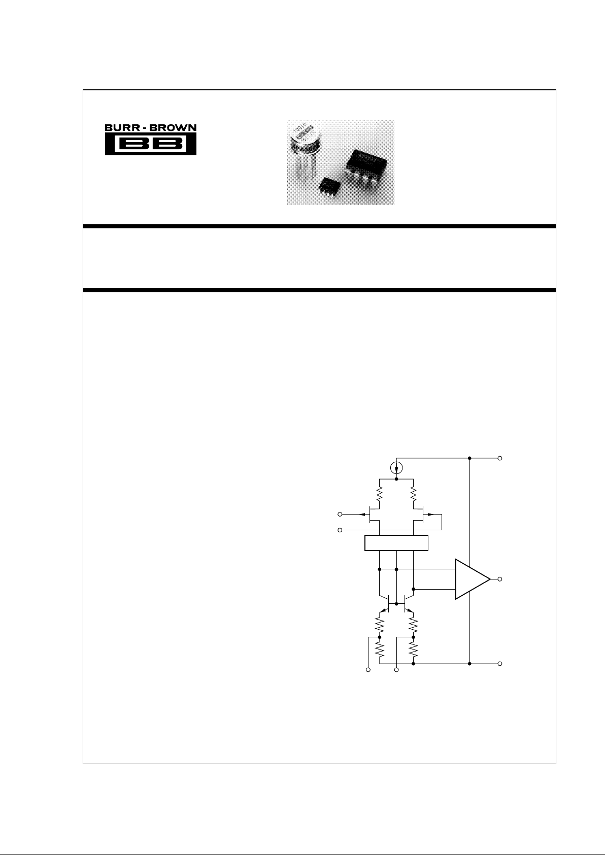
Cascode
–In
(2)
+In
(3)
+V
(7)
S
Output
(6)
–V
(4)
S
(1) (5)
OPA602
®
International Airport Industrial Park • Mailing Address: PO Box 11400 • Tucson, AZ 85734 • Street Address: 6730 S. Tucson Blvd. • Tucson, AZ 85706
Tel: (520) 746-1111 • Twx: 910-952-1111 • Cable: BBRCORP • Telex: 066-6491 • FAX: (520) 889-1510 • Immediate Product Info: (800) 548-6132
Difet
®
Burr-Brown Corp.
FEATURES
● WIDE BANDWIDTH: 6.5MHz
● HIGH SLEW RATE: 35V/
µs
● LOW OFFSET:
±250µV max
● LOW BIAS CURRENT:
±1pA max
● FAST SETTLING TIME: 1
µs to 0.01%
● UNITY-GAIN STABLE
DESCRIPTION
The OPA602 is a precision, wide bandwidth FET
operational amplifier. Monolithic
Difet
(dielectrically
isolated FET) construction provides an unusual combination of high speed and accuracy.
Its wide-bandwidth design minimizes dynamic errors.
High slew rate and fast settling time allow accurate
signal processing in pulse and data conversion applications. Wide bandwidth and low distortion minimize
AC errors. All specifications are rated with a 1kΩ
resistor in parallel with 500pF load. The OPA602 is
unity-gain stable and easily drives capacitive loads up
to 1500pF.
Laser-trimmed input circuitry provides offset voltage
and drift performance normally associated with precision bipolar op amps.
Difet
construction achieves
extremely low input bias currents (1pA max) without
compromising input voltage noise.
The OPA602’s unique input cascode circuitry maintains low input bias current and precise input characteristics over its full input common-mode voltage
range.
©
1987 Burr-Brown Corporation PDS-753E Printed in U.S.A. August, 1995
Page 2

2
®
OPA602
OPA602AM/AP/AU OPA602BM/SM/BP OPA602CM
PARAMETER CONDITIONS MIN TYP MAX MIN TYP MAX MIN TYP MAX UNITS
INPUT NOISE
Voltage: f
O
= 10Hz * 23 * nV/√ Hz
f
O
= 100Hz * 19 * nV/√Hz
f
O
= 1kHz * 13 * nV/√Hz
f
O
= 10kHz * 12 * nV/√Hz
f
B
= 10Hz to 10kHz * 1.4 * µVrms
f
B
= 0.1Hz to 10Hz * 0.95 * µVp-p
Current: f
B
= 0.1Hz to 10Hz * 12 * fAp-p
f
O
= 0.1Hz to 20kHz * 0.6 * fA/√Hz
OFFSET VOLTAGE
Input Offset Voltage:
M Package V
CM
= 0VDC ±300 ±1000 ±150 ±500 ±100 ±250 µV
P Package 1 2 0.5 1 mV
U Package 1 3 mV
Over Specified Temperature
M Package ±550 ±250 ±1000 ±200 ±500 µV
P, U Packages ±1.5 ±0.75 ±1.5 mV
Average Drift T
A
= T
MIN
to T
MAX
* ±15 ±3 ±5*±2µV/°C
Supply Rejection ±V
S
= 12V to 18V 70 * 80 100 86 * dB
BIAS CURRENT
Input Bias Current V
CM
= 0VDC ±2 ±10 ±1 ±2 ±0.5 ±1pA
Over Specified Temperature ±20 ±500 ±20 ±200 ±10 ±100 pA
SM Grade ±200 ±2000 pA
OFFSET CURRENT
Input Offset Current V
CM
= 0VDC 1 10 0.5 2 0.5 1 pA
Over Specified Temperature 20 500 20 200 10 100 pA
SM Grade 200 1000 pA
INPUT IMPEDANCE
Differential * 10
13
|| 1 * Ω || pF
Common-Mode * 10
14
|| 3 * Ω || pF
INPUT VOLTAGE RANGE
Common-Mode Input Range * * ±10.2 +13, * * V
–11
Common-Mode Rejection V
IN
= ±10VDC 75 * 88 100 92 * dB
OPEN-LOOP GAIN, DC
Open-Loop Voltage Gain R
L
≥ 1kΩ 75 * 88 100 92 * dB
FREQUENCY RESPONSE
Gain Bandwidth Gain = 100 3.5 * 4 6.5 5 * MHz
Full Power Response 20Vp-p, R
L
= 1kΩ * 570 * kHz
Slew Rate V
O
= ±10V, RL = 1kΩ 20 * 24 35 28 * V/µs
Settling Time: 0.1% Gain = –1, R
L
= 1kΩ * 0.6 * µs
0.01% C
L
= 500pF, 10V Step * 1.0 * µs
RATED OUTPUT
Voltage Output R
L
= 1kΩ±11 * ±11.5 +12.9, * * V
–13.8
Current Output V
O
= ±10VDC * * ± 15 ±20 * * mA
Output Resistance 1MHz, Open Loop * 80 * Ω
Load Capacitance Stability Gain = +1 * 1500 * pF
Short Circuit Current ±25 * ±30 ±50 * * mA
POWER SUPPLY
Rated Voltage * ±15 * VDC
Voltage Range,
Derated Performance * * ±5 ±18 * * VDC
Current, Quiescent I
O
= 0mADC * * 3 4 * * mA
Over Specified Temperature * * 3.5 4.5 * * mA
TEMPERATURE RANGE
Specification Ambient Temperature * * –25 +85 * * °C
SM Grade –55 +125 °C
Operating: M Package Ambient Temperature * * –55 +125 * * °C
P, U Packages –25 +85 –25 +85 °C
Storage: M Package Ambient Temperature * * –65 +150 * * °C
P, U Packages –40 +125 –40 +125 °C
θ
JA
* 200 * °C/W
SPECIFICATIONS
ELECTRICAL
At VS = ±15VDC and TA = +25°C unless otherwise noted.
* Same specifications as OPA602BM.
Page 3
®
OPA602
3
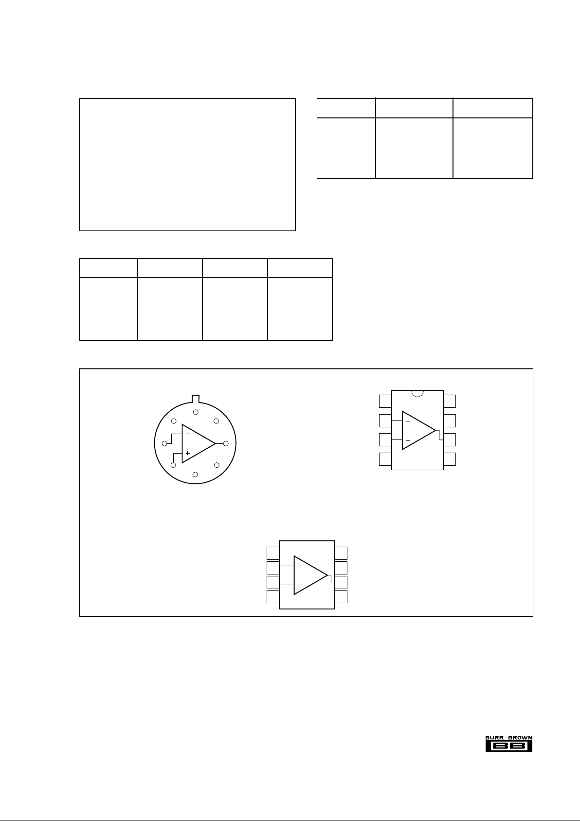
PIN CONFIGURATIONS
ABSOLUTE MAXIMUM RATINGS
Supply Voltage.............................................................................. ±18VDC
Internal Power Dissipation (T
J
≤ +175°C) .................................... 1000mW
Differential Input Voltage............................................................... Total V
S
Input Voltage Range ............................................................................ ±V
S
Storage Temperature Range
M Package .................................................................. –65°C to +150°C
P and U Packages ....................................................... –40°C to +125°C
Operating Temperature Range
M Package .................................................................. –55°C to +125°C
P and U Packages ........................................................ –25°C to + 85°C
Lead Temperature
M and P Packages (soldering, 10s) ............................................ +300°C
U Package, SOIC (3s) ................................................................+260°C
Output Short Circuit to Ground (+25°C) ................................... Continuous
Junction Temperature .................................................................... +175°C
8
7
1
4
53
2
6
–V
S
+V
S
NC
Offset Trim
Output
Offset Trim
–In
+In
Case Connected to +V
S.
Top View — TO-99
8
7
5
6
+V
S
Output
Offset Trim
NC
Top View — DIP
1
2
4
3
–In
+In
–V
S
Offset Trim
The information provided herein is believed to be reliable; however, BURR-BROWN assumes no responsibility for inaccuracies or omissions. BURR-BROWN assumes
no responsibility for the use of this information, and all use of such information shall be entirely at the user’s own risk. Prices and specifications are subject to change
without notice. No patent rights or licenses to any of the circuits described herein are implied or granted to any third party. BURR-BROWN does not authorize or warrant
any BURR-BROWN product for use in life support devices and/or systems.
1
2
3
4
8
7
6
5
NC
+V
S
Output
Offset Trim
Offset Trim
–In
+In
–V
S
Top View — SOIC
ORDERING INFORMATION
TEMPERATURE OFFSET VOLTAGE
MODEL PACKAGE RANGE MAX (
µV) AT 25°C
OPA602AM TO-99 –25 to +85°C ±1000
OPA602BM TO-99 –25 to +85°C ±500
OPA602CM TO-99 –25 to +85°C ±250
OPA602SM TO-99 –55 to +125°C ±500
OPA602AP Plastic DIP –25 to +85°C ±2000
OPA602BP Plastic DIP –25 to +85°C ±1000
OPA602AU Plastic SOIC –25 to +85°C ±3000
PACKAGE INFORMATION
PACKAGE DRAWING
MODEL PACKAGE NUMBER
(1)
OPA602AM TO-99 001
OPA602BM TO-99 001
OPA602CM TO-99 001
OPA602SM TO-99 001
OPA602AP Plastic DIP 006
OPA602BP Plastic DIP 006
OPA602AU Plastic SOIC 182
NOTE: (1) For detailed drawing and dimension table, please see end of data
sheet, or Appendix C of Burr-Brown IC Data Book.
Page 4

4
®
OPA602
E
O
R
S
TOTAL INPUT VOLTAGE NOISE SPECTRAL DENSITY
AT 1kHz vs SOURCE RESISTANCE
1k
100
10
1
100 1k 10k 100k 1M 10M 100M
Source Resistance ( )
Ω
Voltage Noise, E (nV/√Hz)
O
OPA602 + Resistor
Resistor Noise Only
POWER SUPPLY REJECTION AND COMMON-MODE
REJECTION vs TEMPERATURE
110
–75
Temperature (°C)
CMR and PSR (dB)
105
100
95
90
–50 –25 0 25 50 75 100 125
CMR
PSR
INPUT VOLTAGE NOISE SPECTRAL DENSITY
1k
100
10
1
1 10 100 1k 10k 100k 1M
Frequency (Hz)
Voltage Noise (nV/√Hz)
INPUT CURRENT NOISE SPECTRAL DENSITY
100
10
1
0.1
1 10 100 1k 10k 100k 1M
Frequency (Hz)
Current Noise (fA/√Hz)
DICE INFORMATION
TYPICAL PERFORMANCE CURVES
TA = +25°C, VS = ±15VDC unless otherwise noted.
MECHANICAL INFORMATION
MILS (0.001") MILLIMETERS
Die Size 63 x 58 ±5 1.60 x 1.47 ±0.13
Die Thickness 20 ±3 0.51 ±0.08
Min. Pad Size 4 x 4 0.10 x 0.10
Backing None
Transistor Count 36
PAD FUNCTION
1 Offset Trim
2 –In
3 +In
4–V
S
5 Offset Trim
6 Output
7+V
S
Substrate Bias: –V
S
NC: No Connection.
OPA602 DIE TOPOGRAPHY
5
4
3
2
6
7
1
Page 5

®
OPA602
5
MAXIMUM OUTPUT VOLTAGE SWING
vs FREQUENCY
30
10k 100k 1M 10M
Frequency (Hz)
Output Voltage (V p-p)
20
10
0
RL = 1kΩ
OPEN-LOOP GAIN vs TEMPERATURE
120
–75
Ambient Temperature (°C)
Voltage Gain (dB)
110
100
90
80
–50 –25 0 25 50 75 100 125
GAIN BANDWIDTH AND SLEW RATE
vs SUPPLY VOLTAGE
8
0
Supply Voltage (±V
CC
)
Gain Bandwidth (MHz)
Slew Rate (V/µs)
5
5 101520
38
32
7
6
36
34
AV = –1
GBW
Slew Rate
GAIN BANDWIDTH AND SLEW RATE
vs TEMPERATURE
10
–75
Ambient Temperature (°C)
Gain Bandwidth (MHz)
Slew Rate (V/µs)
8
6
4
2
–50 –25 0 25 50 75 100 125
37
35
33
31
29
GBW
Slew Rate
OPEN-LOOP FREQUENCY RESPONSE
140
1
Frequency (Hz)
Voltage Gain (dB)
10 100 1k 10k 100k 1M 10M
120
100
80
60
40
20
0
–45
–90
–135
–180
Phase Shift (Degrees)
R = 1kΩ
C = 100pF
L
L
A
OL
φ
COMMON-MODE REJECTION
vs INPUT COMMON-MODE VOLTAGE
120
–15 –10 –5 0 +5 +10 +15
Common-Mode Rejection (dB)
Common-Mode Voltage (V)
110
100
90
80
70
TYPICAL PERFORMANCE CURVES (CONT)
TA = +25°C, VS = ±15VDC unless otherwise noted.
Page 6

6
®
OPA602
Output Voltage (V)
50
LARGE SIGNAL TRANSIENT RESPONSE
Time (µs)
1234
10
0
–10
TOTAL HARMONIC DISTORTION
vs FREQUENCY
1
0.1
0.01
0.001
0.1
Frequency (Hz)
THD + Noise (%rms)
1 10 100 1k 10k 100k
6.5Vrms
1kΩ
402Ω
40.2kΩ
AV = +101V/V
A = +101V/V
V
A = +1V/V
V
OPEN-LOOP GAIN vs SUPPLY VOLTAGE
104
0
Supply Voltage (±V
CC
)
Voltage Gain
92
5 101520
100
96
SETTLING TIME vs CLOSED-LOOP GAIN
5
4
3
2
1
0
–1 –10 –100 –1k
Closed-Loop Gain (V/V)
Settling Time (µs)
0.1%
R = 1kΩ
C = 100pF
L
L
0.01%
SUPPLY CURRENT vs TEMPERATURE
3.5
3.25
3.0
2.75
2.5
–75
Ambient Temperature (°C)
Supply Current (mA)
–50 –25 0 25 50 75 100 125
TYPICAL PERFORMANCE CURVES (CONT)
TA = +25°C, VS = ±15VDC unless otherwise noted.
Output Voltage (mV)
120
SMALL SIGNAL TRANSIENT RESPONSE
Time (µs)
110
100
50
0
–50
–100
–150
Page 7

®
OPA602
7
COMMON-MODE REJECTION
vs FREQUENCY
140
1
Frequency (Hz)
Common-Mode Rejection (dB)
10 100 1k 10k 100k 1M 10M
120
100
80
60
40
20
0
POWER SUPPLY REJECTION
vs FREQUENCY
140
1
Frequency (Hz)
Power Supply Rejection (dB)
10 100 1k 10k 100k 1M 10M
120
100
80
60
40
20
0
+–
BIAS AND OFFSET CURRENT
vs INPUT COMMON MODE VOLTAGE
10
1
0.1
0.01
Bias Current (pA)
–15
Common-Mode Voltage (V)
10
1
0.1
0.01
Offset Current (pA)
–10 –5 0 5 10 15
Bias Current
Offset Current
BIAS AND OFFSET CURRENT
vs TEMPERATURE
10nA
Bias Current (pA)
–50
Ambient Temperature (°C)
10nA
Offset Current (pA)
–25 0 25 50 75 100 125
1nA
100
10
1
0.1
1nA
100
10
1
0.1
TYPICAL PERFORMANCE CURVES (CONT)
TA = +25°C, VS = ±15VDC unless otherwise noted.
APPLICATIONS INFORMATION
Unity-gain stability with good phase margin and excellent
output drive characteristics bring freedom from the subtle
problems associated with other high speed amplifiers. But
with any high speed, wide bandwidth circuitry, careful
circuit layout will ensure best performance. Make short,
direct interconnections and avoid stray wiring capacitance—
especially at the inverting input pin.
Power supplies should be bypassed with good high frequency capacitors positioned close to the op amp pins. In
most cases 0.1µF ceramic capacitors are adequate. Applications with heavier loads and fast transient waveforms may
benefit from use of additional 1.0µF tantalum bypass capacitors.
INPUT BIAS CURRENT GUARDING
Leakage currents across printed circuit boards can easily
exceed the input bias current of the OPA602. A circuit board
“guard” pattern (Figure 1) is an effective solution to difficult
leakage problems. This guard pattern must be repeated on all
layers of a multilayer board. By surrounding critical high
impedance input circuitry with a low impedance circuit
connection at the same potential, leakage currents will flow
harmlessly to the low impedance node.
Input bias current may also be degraded by improper handling or cleaning. Contamination from handling parts and
circuit boards may be cleaned with appropriate solvents and
deionized water. Each rinsing operation should be followed
by a 30-minute bake at +85°C.
Page 8

8
®
OPA602
Board Layout for Input Guarding:
Guard top and bottom of board.
Alternate—use Teflon
®
standoff for sensitive input pins.
Teflon
®
E.I. Du Pont de Nemours & Co.
FIGURE 1. Connection of Input Guard.
2
3
In
Noninverting
6
Out
2
3
In
Inverting
6
Out
2
3
In
Buffer
6
Out
3
2
4
5
6
7
8
1
TO-99 Bottom View
To Guard Drive
OPA602
OPA602
OPA602
V
OUT
= –V
REF
+ + + ••• +
–10V ≤ V
REF
≤ +10V
0 ≤ V
OUT
≤ – V
REF
Where: BN = 1 if the BN digital input is high
B
N
= 0 if the BN digital input is low
APPLICATION CIRCUITS
FIGURE 2. Offset Voltage Trim.
B
1
B2B
3
B
12
2 4 8 4096
FIGURE 3. Voltage Output D/A Converter.
4095
4096
3
6
2
OPA602
5
1
4
7
+V
S
–V
S
(1)
±10mV Typical
Trim Range
NOTE: (1) 10k to 1M Trim
Potentiometer (100k
Recommended)
Ω
Ω
Ω
2
OPA602
V
OUT
4 5 6 7 8 9 10 11 12 13 14 15
DAC7541A
16
17
V
REFERENCE
+15V
Out 2
R
F
Out 1
C
1
15pF
3
–V
CC
B1••••••••••B
12
MSB
1
18
Single-Point Ground
100k
Ω
()
Page 9

®
OPA602
9
FIGURE 4. Settling Time and Slew Rate Test Circuit.
Output
+15V
2kΩ
47pF
2kΩ
–15V
OPA602
High Quality
Pulse Generator
Pulse in
±5V
2kΩ
1µF Tantalum
1µF Tantalum
+
+
2kΩ
51Ω
CL
500pF
1µF
+
+
+
1µF
1µF
1µF
(2)
HP 5082-2835
+15V
1/2 2N5564
1/2 2N5564
–15V
+
510Ω
510Ω
50Ω
Error Out
±0.5mV
(0.01%)
 Loading...