

Page 1
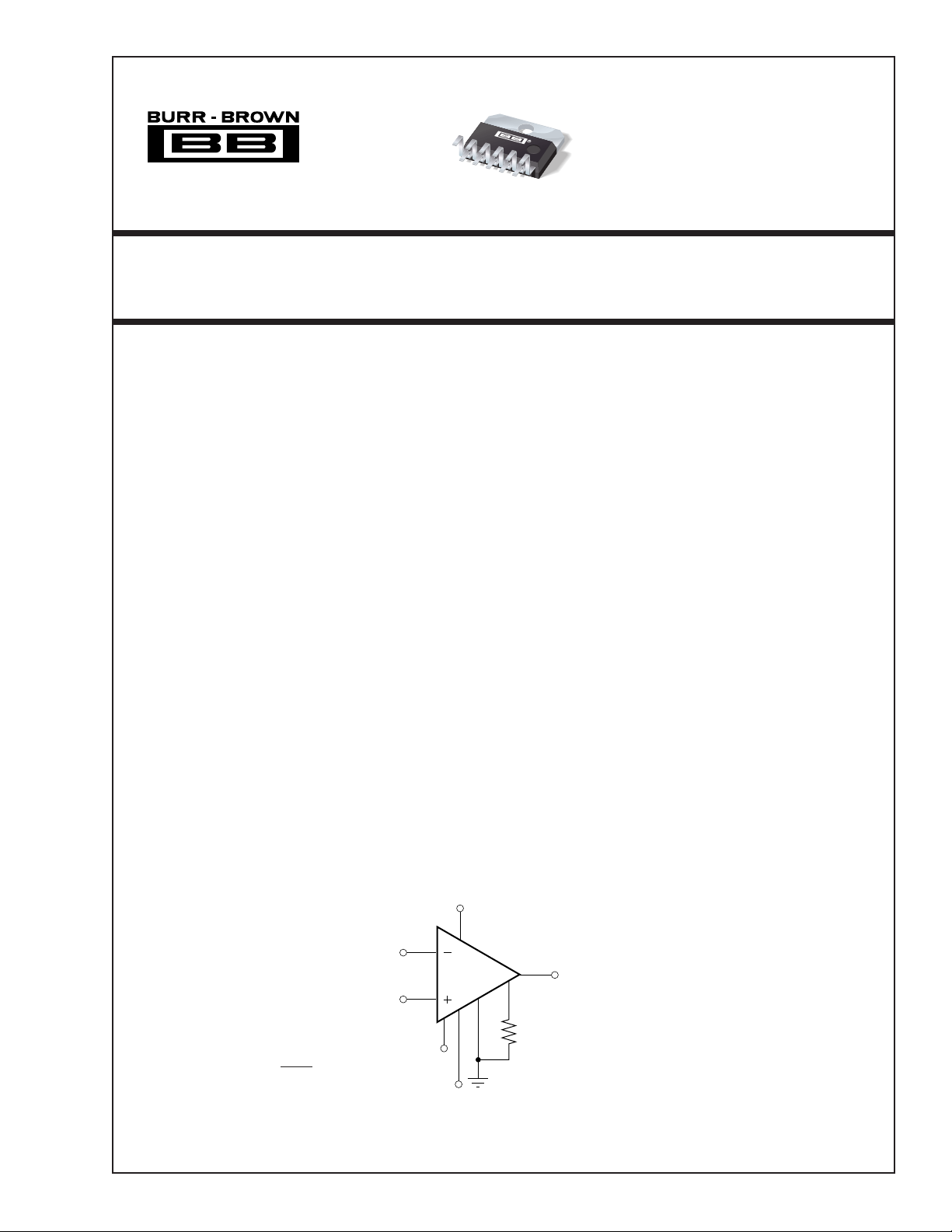
®
For most current data sheet and other product
information, visit www.burr-brown.com
High-Voltage, High-Current
OPERATIONAL AMPLIFIER
OPA549
OPA549
FEATURES
● HIGH OUTPUT CURRENT:
8A Continuous
10A Peak
● WIDE POWER SUPPLY RANGE:
Single Supply: +8V to +60V
Dual Supply: ±4V to ±30V
● WIDE OUTPUT VOLTAGE SWING
● FULLY PROTECTED:
Thermal Shutdown
Adjustable Current Limit
● OUTPUT DISABLE CONTROL
● THERMAL SHUTDOWN INDICATOR
● HIGH SLEW RATE: 9V/µs
● CONTROL REFERENCE PIN
● 11-LEAD POWER ZIP PACKAGE
APPLICATIONS
● VALVE, ACTUATOR DRIVER
● SYNCHRO, SERVO DRIVER
● POWER SUPPLIES
● TEST EQUIPMENT
● TRANSDUCER EXCITATION
● AUDIO POWER AMPLIFIER
DESCRIPTION
The OPA549 is a low-cost, high-voltage/high-current
operational amplifier ideal for driving a wide variety
of loads. This laser-trimmed monolithic integrated
circuit provides excellent low-level signal accuracy,
and high output voltage and current.
The OPA549 operates from either single or dual supplies for design flexibility. The input common-mode
range extends below the negative supply.
The OPA549 is internally protected against overtemperature conditions and current overloads. In addition, the OPA549 provides an accurate, user-selected
current limit. Unlike other designs which use a “power”
resistor in series with the output current path, the
OPA549 senses the load indirectly. This allows the
current limit to be adjusted from 0A to 10A with a
resistor/potentiometer, or controlled digitally with a
voltage-out or current-out DAC.
The Enable/Status (E/S) pin provides two functions. It
can be monitored to determine if the device is in
thermal shutdown, and it can be forced low to disable
the output stage and effectively disconnect the load.
The OPA549 is available in an 11-lead power ZIP
package. Its copper tab allows easy mounting to a heat
sink for excellent thermal performance. Operation is
specified over the extended industrial temperature
range, –40°C to +85°C.
V+
OPA549
ES Pin
Forced Low: Output disabled
Indicates Low: Thermal shutdown
International Airport Industrial Park • Mailing Address: PO Box 11400, Tucson, AZ 85734 • Street Address: 6730 S. Tucson Blvd., Tucson, AZ 85706 • Tel: (520) 746-1111
Twx: 910-952-1111 • Internet: http://www.burr-brown.com/ • Cable: BBRCORP • Telex: 066-6491 • FAX: (520) 889-1510 • Immediate Product Info: (800) 548-6132
©
1999 Burr-Brown Corporation PDS-1450A Printed in U.S.A. November, 1999
E/S
V–
I
Ref
1 OPA549
V
LIM
R
O
R
sets the current limit
CL
value from 0A to 10A.
(Very Low Power Dissipation)
CL
®
Page 2
SPECIFICATIONS: VS = ±2.25V to ±18V
Boldface limits apply over the specified temperature range, TA = –40°C to +85°C
At T
= +25°C, VS = ±30V, Ref = 0V, and E/S pin open, unless otherwise noted.
CASE
OPA549T
PARAMETER CONDITION MIN TYP MAX UNITS
OFFSET VOLTAGE V
Input Offset Voltage VCM = 0V, IO = 0 ±1 ±5mV
vs Temperature dV
vs Power Supply PSRR VS = ±4V to ±30V, Ref = V – 25 100 µV/V
INPUT BIAS CURRENT
Input Bias Current
(1)
(2)
vs Temperature T
Input Offset Current I
NOISE
Input Voltage Noise Density e
Current Noise Density i
INPUT VOLTAGE RANGE
Common-Mode Voltage Range: Positive V
Negative V
Common-Mode Rejection Ratio CMRR V
INPUT IMPEDANCE
Differential 10
Common-Mode 109 || 4 Ω || pF
OPEN-LOOP GAIN
Open-Loop Voltage Gain A
FREQUENCY RESPONSE
Gain Bandwidth Product GBW 0.9 MHz
Slew Rate SR G = 1, 50Vp-p Step, R
Full Power Bandwidth See Typical Curve
Settling Time: ±0.1% G = –10, 50V Step 20 µs
Total Harmonic Distortion + Noise
(3)
OUTPUT
Voltage Output, Positive I
Negative IO = –2A (V–) + 1.7 (V–) + 1.4 V
Positive I
Negative IO = –8A (V–) + 4.6 (V–) + 3.9 V
Negative R
Maximum Continuous Current Output: dc
Output Current Limit
Current Limit Range 0 to ±10 A
Current Limit Equation I
Current Limit Tolerance
(1)
Capacitive Load Drive (Stable Operation) C
Output Disabled
Leakage Current Output Disabled See Typical Curve
Output Capacitance Output Disabled 750 pF
OUTPUT ENABLE /STATUS (E/S) PIN
Shutdown Input Mode
High (output enabled) E/S Pin Open or Forced High (Ref) + 2.4 V
V
E/S
Low (output disabled) E/S Pin Forced Low (Ref) + 0.8 V
V
E/S
I
High (output enabled) E/S Pin Indicates High –50 µA
E/S
Low (output disabled) E/S Pin Indicates Low –55 µA
I
E/S
Output Disable Time 1 µs
Output Enable Time 3 µs
Thermal Shutdown Status Output
Normal Operation Sourcing 20µA (Ref) + 2.4 (Ref) + 3.5 V
Thermally Shutdown Sinking 5µA, T
Junction Temperature, Shutdown +160 °C
Reset from Shutdown +140 °C
Ref (Reference Pin for Control Signals)
Voltage Range V– (V+) – 8 V
(2)
Current
POWER SUPPLY
Specified Voltage V
Operating Voltage Range, (V+) – (V–) 8 60 V
Quiescent Current I
Quiescent Current in Shutdown Mode I
TEMPERATURE RANGE
Specified Range –40 +85 °C
Operating Range –40 +125 °C
Storage Range –55 +125 °C
Thermal Resistance,
Thermal Resistance,
NOTES: (1) High-speed test at T
Frequency” in the Typical Performance Curves section for additional power levels. (4) See “Safe Operating Area” (SOA) in the Typical Performance Curves section.
θ
JC
θ
JA
= +25°C. (2) Positive conventional current is defined as flowing into the terminal. (3) See “Total Harmonic Distortion + Noise vs
J
®
THD+N
(4)
(4)
ac
OS
OS
/dT T
I
B
OS
n
n
CM
CM
OL
= –40°C to +85°C ±20 µV/°C
CASE
V
= 0V –100 –500 nA
CM
= –40°C to +85°C ±0.5 nA/°C
CASE
V
= 0V ±5 ±50 nA
CM
f = 1kHz 70 nV/√Hz
f = 1kHz 1 pA/√Hz
Linear Operation (V+) – 3 (V+) – 2.3 V
Linear Operation (V–) – 0.1 (V–) – 0.2 V
= (V–) – 0.1V to (V+) – 3V 80 95 dB
CM
VO = ±25V, RL = 1kΩ 100 110 dB
VO = ±25V, RL = 4Ω 100 dB
f = 1kHz,RL = 4Ω,G = +3, Power = 25W
= 2A (V+) – 3.2 (V+) – 2.7 V
O
= 8A (V+) – 4.8 (V+) – 4.3 V
O
= 8Ω to V– (V–) + 0.3 (V–) + 0.1 V
L
Waveform Cannot Exceed 10A peak
R
LOAD
= 7.5kΩ (I
CL
S
I
Q
Connected to Ref IO = 0 ±26 ±35 mA
LIM
LIM
= ±5A), RL = 4Ω±200 ±500 mA
LIM
Connected to Ref ±6mA
No Heat Sink 30 °C/W
7
|| 6 Ω || pF
= 4Ω 9V/µs
L
0.015 %
±8A
8 Arms
= 15800 • 4.75V/(7500Ω + RCL)A
LIM
See Typical Curve
> 160°C (Ref) + 0.2 (Ref) + 0.8 V
J
–3.5 mA
±30 V
1.4 °C/W
2OPA549
Page 3
ABSOLUTE MAXIMUM RATINGS
(1)
PACKAGE/ ORDERING INFORMATION
Output Current ................................................ See SOA Curve (Figure 6)
Supply Voltage, V+ to V– ................................................................... 60V
Input Voltage Range ....................................... (V–) – 0.5V to (V+) + 0.5V
Input Shutdown Voltage ................................................... Ref – 0.5 to V+
Operating Temperature ..................................................–40 °C to +125°C
Storage Temperature ..................................................... –55°C to +125°C
Junction Temperature ...................................................................... 150°C
Lead Temperature (soldering, 10s) ................................................. 300°C
ESD Capability (Human Body Model) ............................................. 2000V
NOTE: (1) Stresses above these ratings may cause permanent damage.
Exposure to absolute maximum conditions for extended periods may degrade device reliability.
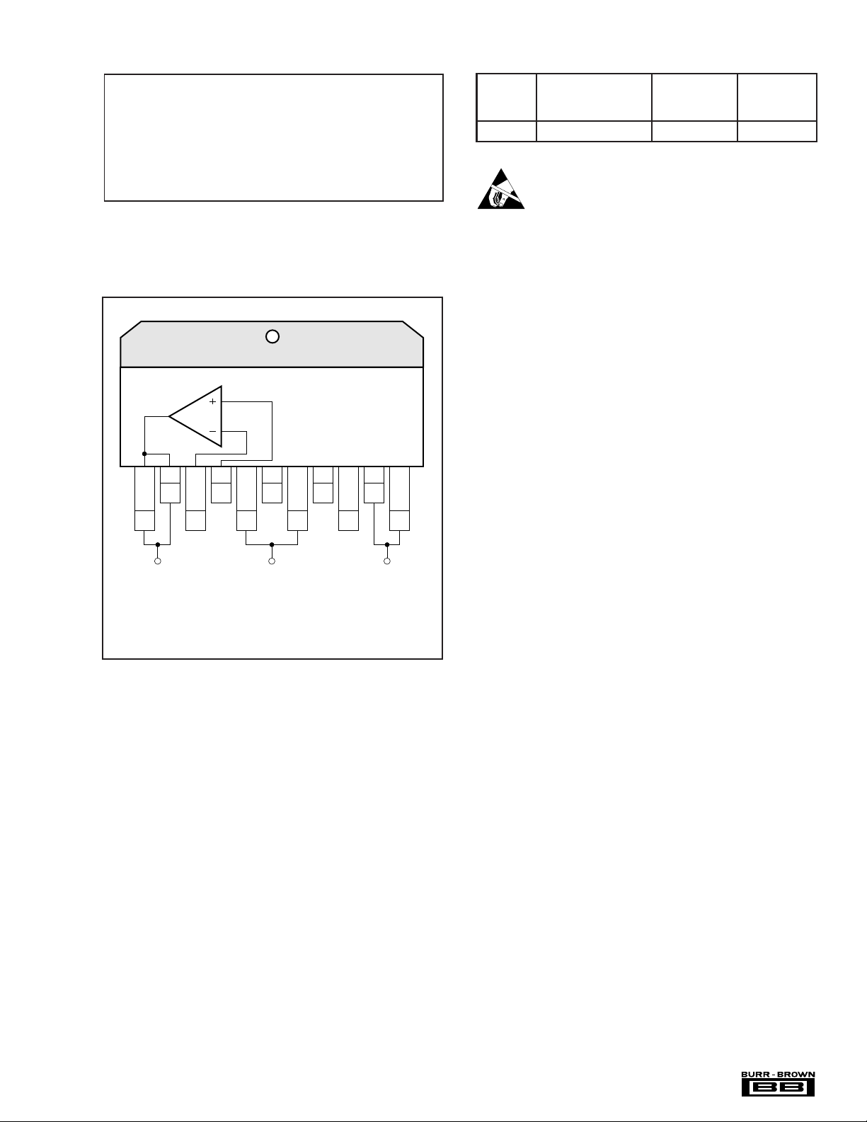
CONNECTION DIAGRAM
Tab connected to V–. Do not use to conduct current.
246810
1357911
+In
–In
Ref I
LIM
E/S
PACKAGE
DRAWING TEMPERATURE
PRODUCT PACKAGE NUMBER RANGE
OPA549T 11-Lead Power ZIP 242 –40°C to +85°C
ELECTROSTATIC
DISCHARGE SENSITIVITY
This integrated circuit can be damaged by ESD. Burr-Brown
recommends that all integrated circuits be handled with
appropriate precautions. Failure to observe proper handling
and installation procedures can cause damage.
ESD damage can range from subtle performance degradation to complete device failure. Precision integrated circuits
may be more susceptible to damage because very small
parametric changes could cause the device not to meet its
published specifications.
O
Connect both pins 1 and 2 to output.
Connect both pins 5 and 7 to V–.
Connect both pins 10 and 11 to V+.
V–
V+V
The information provided herein is believed to be reliable; however, BURR-BROWN assumes no responsibility for inaccuracies or omissions. BURR-BROWN assumes
no responsibility for the use of this information, and all use of such information shall be entirely at the user’s own risk. Prices and specifications are subject to change
without notice. No patent rights or licenses to any of the circuits described herein are implied or granted to any third party. BURR-BROWN does not authorize or warrant
any BURR-BROWN product for use in life support devices and/or systems.
3 OPA549
®
Page 4
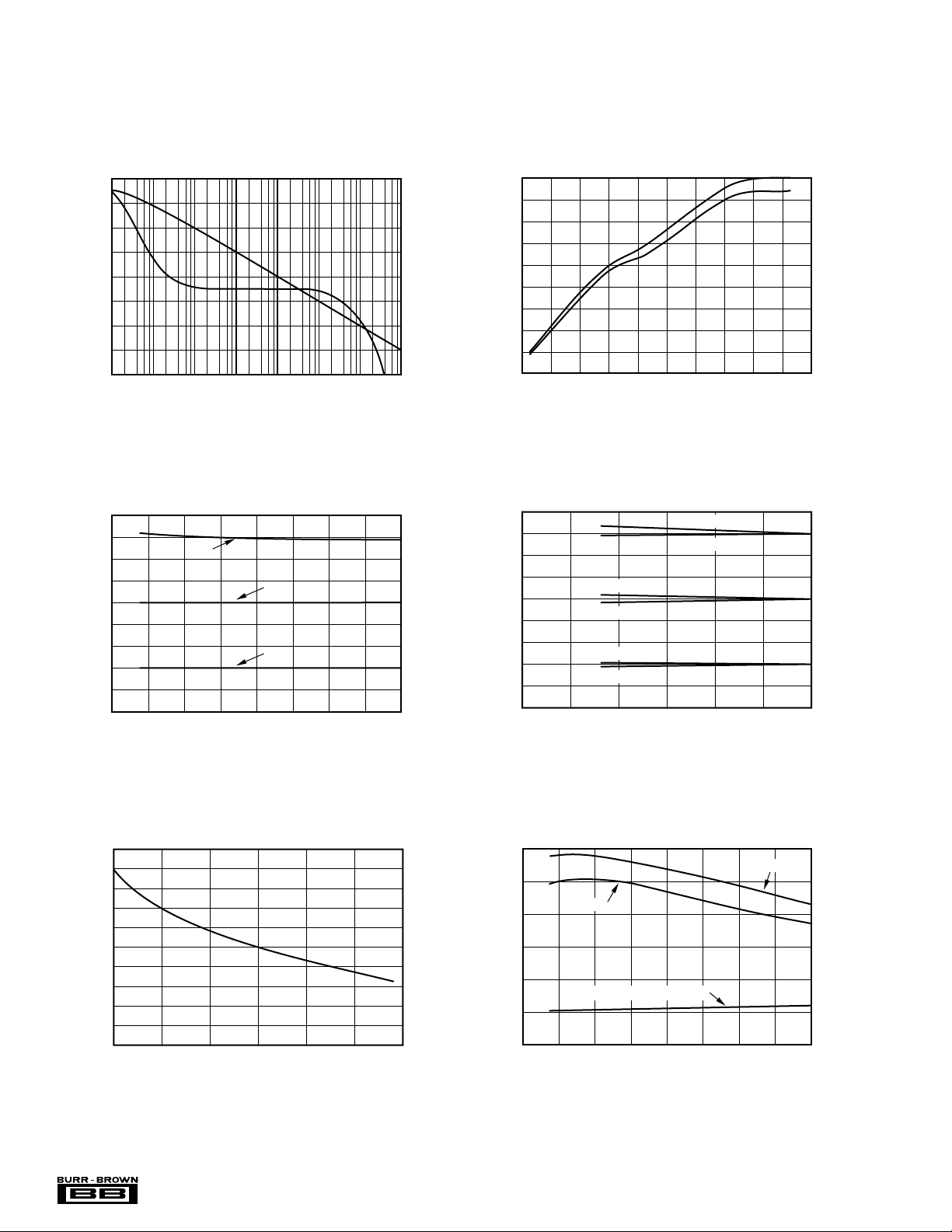
TYPICAL PERFORMANCE CURVES
At T
= +25°C, VS = ±30V and E/S pin open, unless otherwise noted.
CASE
OPEN-LOOP GAIN AND PHASE
vs FREQUENCY
120
100
80
60
40
Gain (dB)
20
0
–20
–40
1 10 100 1k 10k 100k 1M 10M
Frequency (Hz)
CURRENT LIMIT vs TEMPERATURE
9
8
7
6
8A
5A
5
4
3
Current Limit (A)
2A
2
1
0
–75 –50 –25 0 25 50 75 100 125
Temperature (°C)
0
–20
–40
–60
–80
–100
–120
–140
–160
–130
–120
–110
–100
–90
–80
Phase (°)
–70
Input Bias Current (nA)
–60
–50
–40
–60 –40 –20 0 20 40 60 80 140120100
9
8
7
6
5
4
3
Current Limit (A)
2
1
0
0 5 10 15 20 25 30
INPUT BIAS CURRENT vs TEMPERATURE
–I
B
+I
B
Temperature (°C)
CURRENT LIMIT vs SUPPLY VOLTAGE
+I
, 8A
LIM
–I
, 8A
LIM
+I
, 5A
LIM
–I
, 5A
LIM
+I
, 2A
LIM
–I
, 2A
LIM
Supply Voltage (V)
INPUT BIAS CURRENT
vs COMMON-MODE VOLTAGE
–200
–180
–160
–140
–120
–100
–80
–60
Input Bias Current (nA)
–40
–20
–0
–30 –20 –10 0 10 20 30
Common-Mode Voltage (V)
®
30
QUIESCENT CURRENT vs TEMPERATURE
VS = ±30V
25
20
VS = ±5V
15
10
Quiescent Current (mA)
5
IQ Shutdown (output disabled)
0
–75 –50 –25 0 25 50 75 100 125
Temperature (°C)
4OPA549
Page 5
TYPICAL PERFORMANCE CURVES (Cont.)
10 100 1k 10k 100k 1M
120
100
80
60
40
20
0
Power Supply Rejection Ratio (dB)
Frequency (Hz)
POWER SUPPLY REJECTION RATIO
vs FREQUENCY
–PSRR
+PSRR
At T
= +25°C, VS = ±30V and E/S pin open, unless otherwise noted.
CASE
COMMON-MODE REJECTION RATIO vs FREQUENCY
100
90
80
70
60
50
Common-Mode Rejection (dB)
40
10 100 1k 10k 100k
Frequency (Hz)
OPEN-LOOP GAIN, COMMON-MODE REJECTION RATIO
300
VOLTAGE NOISE DENSITY vs FREQUENCY
120
AND POWER SUPPLY REJECTION RATIO
vs TEMPERATURE
250
200
150
100
Voltage Noise (nV/√Hz)
50
0
1 10 100 1k 10k 100k
Frequency (Hz)
GAIN-BANDWIDTH PRODUCT AND
1
0.9
0.8
0.7
0.6
0.5
0.4
0.3
0.2
Gain-Bandwidth Product (MHz)
0.1
0
–75 –50 –25 0 25 50 75 100 125
SLEW RATE vs TEMPERATURE
GBW
SR+
Temperature (°C)
SR–
16
15
14
13
12
11
10
Slew Rate (V/µs)
9
8
7
6
110
100
, CMRR, PSRR (dB)
OL
90
A
80
–75 –50 0 50 100
TOTAL HARMONIC DISTORTION + NOISE
1
G = +3
R
= 4Ω
L
0.1
0.1W
THD+N (%)
0.01
0.001
20 100 1k 10k 20k
A
OL
PSRR
CMRR
Temperature (°C)
vs FREQUENCY
1W
Frequency (Hz)
75W
10W
125
®
5 OPA549
Page 6

TYPICAL PERFORMANCE CURVES (Cont.)
At T
= +25°C, VS = ±30V and E/S pin open, unless otherwise noted.
CASE
OUTPUT VOLTAGE SWING vs OUTPUT CURRENT
5
(V+) –V
O
4
(V)
OUT
3
– V
2
SUPPLY
V
1
(V–) –VO
0
0246810
Output Current (A)
MAXIMUM OUTPUT VOLTAGE SWING
vs FREQUENCY
30
Maximum output
25
20
voltage without
slew rate-induced
distortion.
15
10
Output Voltage (Vp)
5
0
1k 10k 100k 1M
Frequency (Hz)
OUTPUT VOLTAGE SWING vs TEMPERATURE
5
IO = +8A
(V)
OUT
– V
SUPPLY
V
4
3
2
1
IO = –8A
IO = +2A
IO = –2A
0
–75 –50 –25 0 25 50 75 100 125
Temperature (°C)
OUTPUT LEAKAGE CURRENT
vs APPLIED OUTPUT VOLTAGE
5
4
Leakage current with output disabled.
3
2
1
0
–1
–2
Leakage Current (mA)
–3
R
= ∞
CL
R
= 0
CL
–4
–5
–40 –30 –20 –10 0 10 20 4030
Output Voltage (V)
25
PRODUCTION DISTRIBUTION
20
15
10
5
Percent of Amplifiers (%)
0
–4.7
–4.23
–3.76
–3.29
–2.82
®
OFFSET VOLTAGE
–2.35
–1.88
–1.41
–0.94
–0.47
Offset Voltage (mV)
OFFSET VOLTAGE DRIFT
PRODUCTION DISTRIBUTION
25
20
15
10
5
Percent of Amplifiers (%)
0
0
0.47
0.94
1.41
1.88
2.35
2.82
3.29
3.76
4.23
4.7
048
12162024283236404448525660646872768084
Offset Voltage (µV/°C)
6OPA549
Page 7

TYPICAL PERFORMANCE CURVES (Cont.)
At T
= +25°C, VS = ±30V and E/S pin open, unless otherwise noted.
CASE
SMALL-SIGNAL OVERSHOOT
70
60
50
40
30
Overshoot (%)
20
10
0
0 5k 10k 15k 20k 25k 30k 35k
vs LOAD CAPACITANCE
G = +1
G = –1
Load Capacitance (pF)
SMALL-SIGNAL STEP RESPONSE
G = 1, C
= 1000pF
L
10V/div
LARGE-SIGNAL STEP RESPONSE
G = 3, C
= 1000pF
L
5µs/div
SMALL-SIGNAL STEP RESPONSE
G = 3, C
= 1000pF
L
50mV/div
2.5µs/div
100mV/div
2.5µs/div
7 OPA549
®
Page 8

APPLICATIONS INFORMATION
Figure 1 shows the OPA549 connected as a basic noninverting amplifier. The OPA549 can be used in virtually
any op amp configuration.
Power supply terminals should be bypassed with low series
impedance capacitors. The technique shown, using a ceramic and tantalum type in parallel, is recommended. Power
supply wiring should have low series impedance.
Be sure to connect both output pins (pins 1 and 2).
V+
10µF
+
(2)
0.1µF
R
V–
6
0.1µF
10µF
9
Ref
+
2
E/S
1, 2
8
(1)
I
LIM
(2)
V
Z
L
G = 1+
O
R
2
R
1
R
1
10, 11
3
OPA549
V
IN
NOTE: (1) I
current limit, 10A (peak). (2) Connect capacitors directly to
package power supply pins.
4
5, 7
connected to Ref gives the maximum
LIM
FIGURE 1. Basic Circuit Connections.
POWER SUPPLIES
The OPA549 operates from single (+8V to +60V) or dual
(±4V to ±30V) supplies with excellent performance. Most
behavior remains unchanged throughout the full operating
voltage range. Parameters that vary significantly with operating voltage are shown in the Typical Performance Curves.
Some applications do not require equal positive and negative
output voltage swing. Power supply voltages do not need to
be equal. The OPA549 can operate with as little as 8V
between the supplies and with up to 60V between the
supplies. For example, the positive supply could be set to
55V with the negative supply at –5V. Be sure to connect
both V– pins (pins 5 and 7) to the negative power supply
and both V+ pins (pins 10 and 11) to the positive power
supply. Package tab is internally connected to V–, however, do use the tab to conduct current.
CONTROL REFERENCE (Ref) PIN
The OPA549 features a reference (ref) pin to which the I
LIM
and the Enable/Status (E/S) pin are referred. Ref simply
provides a reference point accessible to the user that can be
set to V–, ground, or any reference of the user’s choice.
Ref cannot be set below the negative supply or above (V+) – 8V.
If the minimum VS is used, Ref must be set at V–.
ADJUSTABLE CURRENT LIMIT
The OPA549’s accurate, user-defined current limit can be
set from 0A to 10A by controlling the input to the I
LIM
pin.
Unlike other designs, which use a power resistor in series
with the output current path, the OPA549 senses the load
indirectly. This allows the current limit to be set with a 0µA
to 633µA control signal. In contrast, other designs require a
limiting resistor to handle the full output current (up to 10A
in this case).
Although the design of the OPA549 allows output currents
up to 10A, it is not recommended that the device be operated
continuously at that level. The highest rated continuous
current capability is 8A. Continuously running the OPA549
at output currents greater than 8A will degrade long-term
reliability.
Operation of the OPA549 with current limit less than 1A
results in reduced current limit accuracy. Applications requiring lower output current may be better suited to the
OPA547 or OPA548.
Resistor-Controlled Current Limit
Figure 2a shows a simplified schematic of the internal
circuitry used to set the current limit. Leaving the I
LIM
pin
open programs the output current to zero, while connecting
I
directly to Ref programs the maximum output current
LIM
limit, typically 10A.
With the OPA549, the simplest method for adjusting the
current limit uses a resistor or potentiometer connected
between the I
pin and Ref according to Equation 1:
LIM
75kV
R
=Ω
CL
– 7.5k
I
LIM
(1)
Commonly used values are shown in Figure 2.
Digitally-Controlled Current Limit
The low-level control signal (0µA to 633µA) also allows the
current limit to be digitally controlled by setting either a
current (I
adjusted by varying I
) or voltage (V
SET
). The output current I
SET
according to Equation 2:
SET
I
= I
LIM
/15800
SET
LIM
can be
(2)
Figure 2b demonstrates a circuit configuration implementing this feature.
The output current I
can be adjusted by varying V
LIM
SET
according to Equation 3:
V
= (Ref) + 4.75V – (7500Ω)(I
SET
)/15800 (3)
LIM
Figure 11 demonstrates a circuit configuration implementing this feature.
®
8OPA549
Page 9

OPA549
E/S
CMOS or TTL
Ref
Logic
Ground
(a) RESISTOR METHOD
4.75V
7500Ω
Max I
±I
= I
O
LIM
(4.75) (15800)
=
LIM
7500Ω + R
(b) DAC METHOD (Current or Voltage)
Max IO = I
±I
CL
4.75V
I
7500Ω
SET
LIM
=15800 I
LIM
SET
8
15800 (4.75V)
R
=
CL
=
6
I
LIM
75kΩ
I
LIM
Ref
– 7500Ω
– 7.5kΩ
R
0.01µF
CL
(optional, for noisy
environments)
OPA549 CURRENT LIMIT: 0A to 10A
DESIRED
CURRENT LIMIT
(2)
0A
2.5A
3A
4A
5A
6A
7A
8A
9A
10A
NOTES: (1) Resistors are nearest standard 1% values. (2) Offset in the current limit circuitry
may introduce approximately ±0.25A variation at low current limit values.
FIGURE 2. Adjustable Current Limit.
RESISTOR
(RCL)
I
Open
LIM
22.6kΩ
17.4kΩ
11.3kΩ
7.5kΩ
4.99kΩ
3.24kΩ
1.87kΩ
845Ω
I
Connected to Ref
LIM
8
Ref
6
I
= I
/15800
SET
LIM
V
= (Ref) + 4.75V – (7500Ω) (I
SET
(1)
CURRENT
)
(I
SET
0µA
158µA
190µA
253µA
316µA
380µA
443µA
506µA
570µA
633µA
(Ref) + 4.75V
(Ref) + 3.56V
(Ref) + 3.33V
(Ref) + 2.85V
(Ref) + 2.38V
(Ref) + 1.90V
(Ref) + 1.43V
(Ref) + 0.95V
(Ref) + 0.48V
VOLTAGE
(V
)
SET
(Ref)
D/A
LIM
)/15800
ENABLE/STATUS (E/S) PIN
The Enable/Status Pin provides two unique functions:
1) output disable by forcing the pin low and 2) thermal
shutdown indication by monitoring the voltage level at the
pin. Either or both of these functions can be utilized in an
application. For normal operation (output enabled), the E/S
pin can be left open or driven high (at least 2.4V above Ref).
A small value capacitor connected between the E/S pin and
C
may be required for noisy applications.
REF
Output Disable
To disable the output, the E/S pin is pulled to a logic low
(no greater than 0.8V above Ref). Typically the output is
shut down in 1µs. To return the output to an enabled state,
the E/S pin should be disconnected (open) or pulled to at
least 2.4V above Ref. It should be noted that driving the E/
S pin high (output enabled) does not defeat internal ther-
mal shutdown; however, it does prevent the user from
monitoring the thermal shutdown status. See Figure 3 for
an example implementing this function.
This function not only conserves power during idle periods
(quiescent current drops to approximately 6mA) but also
allows multiplexing in multi-channel applications. Figure 12
FIGURE 3. Output Disable.
shows two OPA549s in a switched amplifier configuration.
The on/off state of the two amplifiers is controlled by the
voltage on the E/S pin. Under these conditions, the disabled
device will behave like a 750pF load. Slewing faster than
3V/µs will cause leakage current to rapidly increase in
devices that are disabled, and will contribute additional load.
At high temperature (125°C), the slewing threshold drops to
approximately 2V/µs. Input signals must be limited to avoid
excessive slewing in multiplexed applications.
®
9 OPA549
Page 10

Thermal Shutdown Status
The OPA549 has thermal shutdown circuitry that protects
the amplifier from damage. The thermal protection circuitry
disables the output when the junction temperature reaches
approximately 160°C and allows the device to cool. When
the junction temperature cools to approximately 140°C, the
output circuitry is automatically re-enabled. Depending on
load and signal conditions, the thermal protection circuit
may cycle on and off. The E/S pin can be monitored to
determine if the device is in shutdown. During normal
operation, the voltage on the E/S pin is typically 3.5V above
Ref. Once shutdown has occurred, this voltage drops to
approximately 200mV above Ref. See Figure 4 for an
example implementing this function.
The Safe Operating Area (SOA curve, Figure 6) shows the
permissible range of voltage and current.
The safe output current decreases as VS – VO increases.
Output short circuits are a very demanding case for SOA. A
short circuit to ground forces the full power supply voltage
(V+ or V–) across the conducting transistor. Increasing the
case temperature reduces the safe output current that can be
tolerated without activating the thermal shutdown circuit of
the OPA549. For further insight on SOA, consult Application Bulletin AB-039.
20
10
OPA549
E/S
Ref
HCT
E/S pin can interface
Logic
Ground
with standard HCT logic
inputs. Logic ground is
referred to Ref.
FIGURE 4. Thermal Shutdown Status.
External logic circuitry or an LED can be used to indicate if
the output has been thermally shutdown, as demonstrated in
Figure 10.
Output Disable and Thermal Shutdown Status
As mentioned earlier, the OPA549’s output can be disabled
and the disable status can be monitored simultaneously.
Figure 5 provides an example of interfacing to the E/S pin.
Open-drain logic output can disable
amplifier's output with logic low.
HCT logic input monitors thermal
OPA549
E/S
Ref
Logic
Ground
shutdown status during normal
operation.
Open Drain
(Output Disable)
(Thermal Status
HCT
Shutdown)
FIGURE 5. Output Disable and Thermal Shutdown Status.
SAFE OPERATING AREA
Stress on the output transistors is determined both by the
output current and by the output voltage across the conducting output transistor, VS – VO. The power dissipated by the
output transistor is equal to the product of the output current
and the voltage across the conducting transistor, VS – VO.
Output current can
be limited to less
than 8A—see text.
1
Output Current (A)
Pulse Operation Only
0.1
(Limit rms current to ≤ 8A)
12 510
V
PD = 47W
PD = 18W
– VO (V)
S
PD = 90W
TC = 85°C
TC = 125°C
20 50 100
TC = 25°C
FIGURE 6. Safe Operating Area.
POWER DISSIPATION
Power dissipation depends on power supply, signal, and load
conditions. For dc signals, power dissipation is equal to the
product of output current times the voltage across the conducting output transistor. Power dissipation can be minimized by using the lowest possible power supply voltage
necessary to assure the required output voltage swing.
For resistive loads, the maximum power dissipation occurs
at a dc output voltage of one-half the power supply voltage.
Dissipation with ac signals is lower. Application Bulletin
AB-039 explains how to calculate or measure power dissipation with unusual signals and loads.
THERMAL PROTECTION
Power dissipated in the OPA549 will cause the junction
temperature to rise. Internal thermal shutdown circuitry
shuts down the output when the die temperature reaches
approximately 160°C and resets when the die has cooled
to 140°C. Depending on load and signal conditions, the
thermal protection circuit may cycle on and off. This limits
the dissipation of the amplifier but may have an undesirable
effect on the load.
Any tendency to activate the thermal protection circuit
indicates excessive power dissipation or an inadequate heat
sink. For reliable operation, junction temperature should be
limited to 125°C maximum. To estimate the margin of safety
®
10OPA549
Page 11

in a complete design (including heat sink) increase the
0 25 50 75 100 125
30
20
10
0
Power Dissipation (W)
Ambient Temperature (°C)
Thermalloy 6396B HA= 5.6°C/W
assume
CH
= 0.5°C/W
OPA549
JC
= 1.4°C/W
JA
= 7.5°C/W
Thermalloy 6396B
HA
= 3.3°C/W
assume
CH
= 0.5°C/W
OPA549
JC
= 1.4°C/W
JA
= 5.2°C/W
θ
θ
θ
θ
θ
θ
θ
θ
with Thermalloy 6396B
Heat Sink,
JA
= 7.5°C/W
θ
with Thermalloy 6399B
Heat Sink,
JA
= 5.2°C/W
θ
PD = (TJ (max) – TA)/
JA
(TJ (max) – 150°C)
θ
with No Heat Sink,
JA
= 30°C/W
θ
ambient temperature until the thermal protection is triggered. Use worst-case load and signal conditions. For good
reliability, thermal protection should trigger more than 35°C
above the maximum expected ambient condition of your
application. This produces a junction temperature of 125°C
at the maximum expected ambient condition.
The internal protection circuitry of the OPA549 was designed to protect against overload conditions. It was not
intended to replace proper heat sinking. Continuously running the OPA549 into thermal shutdown will degrade reliability.
AMPLIFIER MOUNTING AND HEAT SINKING
Most applications require a heat sink to assure that the
maximum operating junction temperature (125°C) is not
exceeded. In addition, the junction temperature should be
kept as low as possible for increased reliability. Junction
temperature can be determined according to the Equations:
TJ = TA + PD
where
θ
=
JA
TJ= Junction Temperature (°C)
TA= Ambient Temperature (°C)
PD= Power Dissipated (W)
θ
= Junction-to-Case Thermal Resistance (°C/W)
JC
θ
= Case-to-Heat Sink Thermal Resistance (°C/W)
CH
θ
= Heat Sink-to-Ambient Thermal Resistance (°C/W)
HA
θ
= Junction-to-Air Thermal Resistance (°C/W)
JA
Figure 7 shows maximum power dissipation versus ambient
temperature with and without the use of a heat sink. Using
a heat sink significantly increases the maximum power
dissipation at a given ambient temperature as shown.
The challenge in selecting the heat sink required lies in
determining the power dissipated by the OPA549. For dc
output, power dissipation is simply the load current times the
voltage developed across the conducting output transistor,
PD = IL (VS – VO). Other loads are not as simple. Consult
Application Bulletin AB-039 for further insight on calculating power dissipation. Once power dissipation for an application is known, the proper heat sink can be selected.
Heat Sink Selection Example—An 11-lead power ZIP
package is dissipating 10 Watts. The maximum expected
ambient temperature is 40°C. Find the proper heat sink to
keep the junction temperature below 125°C (150°C minus
25°C safety margin).
Combining Equations (4) and (5) gives:
TJ, TA, and PD are given.
tions Table, 1.4°C/W (dc).
sink manufacturer. Its value depends on heat sink size, area,
and material used. Semiconductor package type, mounting
TJ = TA + PD (
θ
JA
θ
+
θ
+
CH
θ
CH
+
θ
HA
θ
) (6)
HA
JC
θ
+
JC
θ
is provided in the Specifica-
JC
θ
can be obtained from the heat
CH
screw torque, insulating material used (if any), and thermal
joint compound used (if any) also affect
for a mounted 11-lead power ZIP package is 0.5°C/W. Now
we can solve for
θ
= [(TJ – TA)/ PD] –
HA
θ
= [(125°C – 40°C)/10W] – 1.4°C/W – 0.5°C/W
HA
θ
= 6.6°C/W
HA
θ
:
HA
θ
–
θ
JC
CH
To maintain junction temperature below 125°C, the heat
sink selected must have a
θ
less than 6.6°C/W. In other
HA
words, the heat sink temperature rise above ambient must be
less than 66°C (6.6°C/W • 10W). For example, at 10W
Thermalloy model number 6396B has a heat sink tempera-
ture rise of 56°C (
θ
= 56°C/10W = 5.6°C/W), which is
HA
below the required 66°C required in this example. Thermalloy
model number 6399B has a sink temperature rise of 33°C
(
θ
= 33°C/10W = 3.3°C/W), which is also below the
HA
required 66°C required in this example. Figure 7 shows
(4)
(5)
power dissipation versus ambient temperature for a 11-lead
power ZIP package with the Thermalloy 6396B and 6399B
heat sinks.
FIGURE 7. Maximum Power Dissipation vs Ambient
Temperature.
Another variable to consider is natural convection versus
forced convection air flow. Forced-air cooling by a small fan
can lower
θ
(
θ
+
θ
CA
CH
) dramatically. Some heat sink
HA
manufacturers provide thermal data for both of these cases.
Heat sink performance is generally specified under idealized
conditions that may be difficult to achieve in an actual
application. For additional information on determining heat
sink requirements, consult Application Bulletin AB-038.
11 OPA549
θ
. A typical
CH
θ
CH
®
Page 12

As mentioned earlier, once a heat sink has been selected, the
complete design should be tested under worst-case load and
signal conditions to ensure proper thermal protection. Any
tendency to activate the thermal protection circuitry may
indicate inadequate heat sinking.
The tab of the 11-lead power ZIP package is electrically
connected to the negative supply, V–. It may be desirable to
isolate the tab of 11-lead power ZIP package from its
mounting surface with a mica (or other film) insulator. For
lowest overall thermal resistance, it is best to isolate the
entire heat sink/OPA549 structure from the mounting surface rather than to use an insulator between the semiconductor and heat sink.
OUTPUT STAGE COMPENSATION
The complex load impedances common in power op amp
applications can cause output stage instability. For normal
operation, output compensation circuitry is typically not
required. However, for difficult loads or if the OPA549 is
intended to be driven into current limit, an R/C network may
be required. Figure 8 shows an output R/C compensation
(snubber) network which generally provides excellent stability.
A snubber circuit may also enhance stability when driving
large capacitive loads (>1000pF) or inductive loads (motors,
loads separated from the amplifier by long cables). Typically, 3Ω to 10Ω resistors in series with 0.01µF to 0.1µF
capacitors is adequate. Some variations in circuit values
may be required with certain loads.
OUTPUT PROTECTION
Reactive and EMF-generating loads can return load current
to the amplifier, causing the output voltage to exceed the
power supply voltage. This damaging condition can be
avoided with clamp diodes from the output terminal to the
power supplies as shown in Figure 8. Schottky rectifier
diodes with a 8A or greater continuous rating are recommended.
VOLTAGE SOURCE APPLICATION
Figure 9 illustrates how to use the OPA549 to provide an
accurate voltage source with only three external resistors.
First, the current limit resistor, RCL , is chosen according to
the desired output current. The resulting voltage at the I
LIM
pin is constant and stable over temperature. This voltage,
VCL, is connected to the non-inverting input of the op amp
and used as a voltage reference, thus eliminating the need for
an external reference. The feedback resistors are selected to
gain VCL to the desired output voltage level.
PROGRAMMABLE POWER SUPPLY
A programmable source/sink power supply can easily be
built using the OPA549. Both the output voltage and output
current are user-controlled. Figure 10 shows a circuit using
potentiometers to adjust the output voltage and current while
Figure 11 uses digital-to-analog converters. An LED connected to the E/S pin through a logic gate indicates if the
OPA549 is in thermal shutdown.
V+
OPA549
V–
R
20kΩ
2
R
1
V
5kΩ
IN
D1, D2 : Schottky Diodes
FIGURE 8. Motor Drive Circuit.
D
2
R
2
G = – = –4
R
1
D
1
10Ω
(Carbon)
0.01µF
Motor
R
1
4.75V
I
LIM
V–
R
CL
2kΩ
10
G = = 10
1
V
CL
(Optional, for noisy
0.01µF
environments)
For Example:
If I
= 7.9A, R
LIM
2kΩ • 4.75V
V
= = 1V
CL
(2kΩ + 7500Ω)
Desired V
= 10V,
O
= 1kΩ and R2 = 9kΩ
R
1
7500Ω
CL =
FIGURE 9. Voltage Source.
R
2
V+
VO = V
Ref
Uses voltage developed at I
as a moderately accurate reference
voltage.
IO =
(1 + R2/R1)
CL
15800 (4.75V)
7500Ω + R
LIM
CL
pin
®
12OPA549
Page 13

+5V
9kΩ1kΩ
9kΩ
G = 1 + = 10
1kΩ
V– = 0V
V+ = +30V
Output
Adjust
10kΩ
V–
10.5kΩ
0.12V to 2.5V
499Ω
+5V
1kΩ
I
LIM
3
4
8
OPA549
Ref
9
6
0V to 4.75V
Current
Limit
Adjust
20kΩ
0.01µF
FIGURE 10. Resistor-Controlled Programmable Power Supply.
–5V
(3)
OUTPUT ADJUST
R
FB A
10pF
I
OUT A
AGND A
+5V
1/2
OPA2336
V
REF
V
REF A
1/2 DAC7800/1/2
DAC A
+5V
E/S
74HCT04
R ≥ 250Ω
Thermal
Shutdown Status
9kΩ1kΩ
3
OPA549
4
Ref
8
I
LIM
= 1V to 25V
V
O
= 0 to 10A
I
O
(LED)
V+ = +30V
V– = 0V
G = 10
1, 2
9
E/S
74HCT04
6
V
= 7V to 25V
O
IO = 0A to 10A
R ≥ 250Ω
Thermal
Shutdown Status
(LED)
V
REF B
R
FB B
10pF
I
1/2 DAC7800/1/2
DAC B
DGND
CURRENT LIMIT ADJUST
Choose DAC780X based on digital interface: DAC7800 - 12-bit
interface, DAC7801 - 8-bit interface + 4 bits, DAC7802 - serial interface.
OUT B
AGND B
1/2
OPA2336
FIGURE 11. Digitally-Controlled Programmable Power Supply.
13 OPA549
0.01µF
®
Page 14

R
V
IN1
1
R
2
R
V
E/S
V
IN2
3
Limit output slew rates to ≤ 3V/µs (see text).
FIGURE 12. Switched Amplifier.
OPA549
Ref
R
2
4kΩ
Master
I
LIM
R
1kΩ
1
VIN
OPA549
R
OPA549
0.1Ω
E/S
4
E/S
20A Peak
V
O
G = 5
OPA549
I
LIM
Ref
V
O
R
CL1
R
CL2
Close for high current
(could be open drain
output of a logic gate).
FIGURE 13. Multiple Current Limit Values.
Slave
0.1Ω
OPA549
I
LIM
Ref
FIGURE 14. Parallel Output for Increased Output Current.
®
14OPA549
 Loading...