

Page 1
1
®
OPA4658
FEATURES
● GAIN BANDWIDTH: 900MHz at G = 2
● GAIN OF 2 STABLE
● LOW POWER: 50mW PER AMP
● LOW DIFF GAIN/PHASE ERRORS:
0.015%/0.02
°
● HIGH SLEW RATE: 1700V/µs
● PACKAGE: 14-Pin DIP and SO-14
Quad Wideband, Low Power Current Feedback
OPERATIONAL AMPLIFIER
APPLICATIONS
● MEDICAL IMAGING
● HIGH-RESOLUTION VIDEO
● HIGH-SPEED SIGNAL PROCESSING
● COMMUNICATIONS
● PULSE AMPLIFIERS
● ADC/DAC GAIN AMPLIFIER
● MONITOR PREAMPLIFIER
● CCD IMAGING AMPLIFIER
DESCRIPTION
The OPA4658 is a quad ultra-wideband, low power
current feedback video operational amplifier featuring
high slew rate and low differential gain/phase error.
The current feedback design allows for superior large
signal bandwidth, even at high gains. The low differential gain/phase errors, wide bandwidth and low
quiescent current make the OPA4658 a perfect choice
for numerous video, imaging and communications
applications.
The OPA4658 is internally compensated for stability in
gains of 2 or greater. The OPA4658 is also available in
dual (OPA2658) and single (OPA658) configurations.
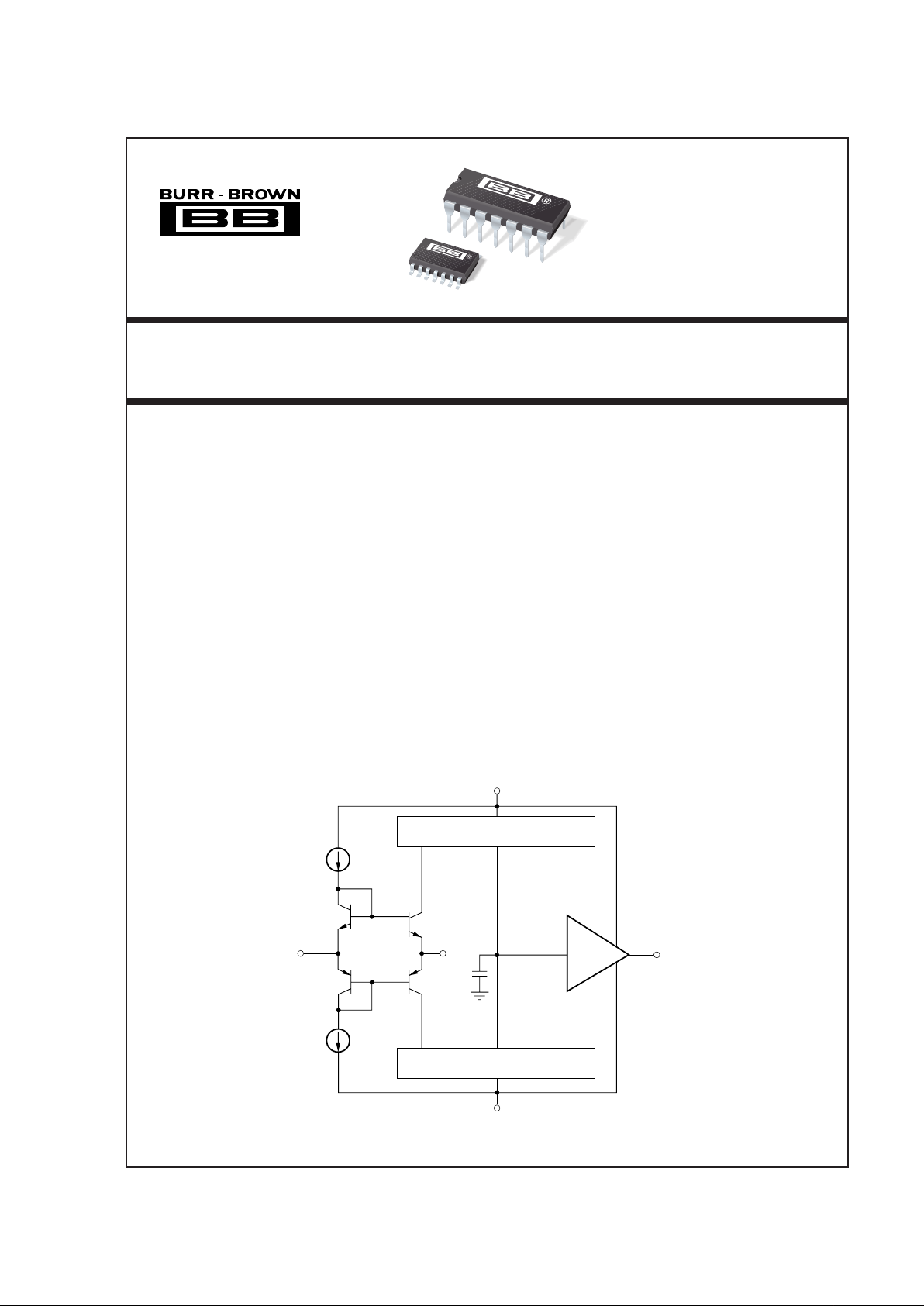
C
COMP
Current Mirror
V
–
V
+
V
OUT
I
BIAS
I
BIAS
+V
S
–V
S
Current Mirror
Buffer
OPA4658
OPA4658
OPA4658
NOTE: Diagram reflects only one-fourth of the OPA4658.
®
International Airport Industrial Park • Mailing Address: PO Box 11400, Tucson, AZ 85734 • Street Address: 6730 S. Tucson Blvd., Tucson, AZ 85706 • Tel: (520) 746-1111 • Twx: 910-952-1111
Internet: http://www.burr-brown.com/ • FAXLine: (800) 548-6133 (US/Canada Only) • Cable: BBRCORP • Telex: 066-6491 • FAX: (520) 889-1510 • Immediate Product Info: (800) 548-6132
© 1994 Burr-Brown Corporation PDS-1270C Printed in U.S.A. March, 1998
Page 2
2
®
OPA4658
FREQUENCY RESPONSE
Closed-Loop Bandwidth
(2)
G = +2 450 ✻
(1)
MHz
G = +5 195 ✻ MHz
G = +10 130 ✻ MHz
Slew Rate
(3)
G = +2, 2V Step 1700 1000 ✻ V/µs
At Minimum Specified Temperature 1500 900 ✻ V/µs
Settling Time: 0.01% G = +2, 2V Step 20 ✻ ns
0.1% G = +2, 2V Step 15.1 ✻ ns
1% G = +2, 2V Step 4.8 ✻ ns
Spurious Free Dynamic Range f = 5MHz, G = +2, V
O
= 2Vp-p 66 ✻ dBc
f = 20MHz, G = +2, V
O
= 2Vp-p 57 ✻ dBc
Third-Order Intercept Point f = 10MHz 38 ✻ dBm
Differential Gain G = +2, NTSC, V
O
= 1.4Vp-p, RL = 150Ω 0.015 ✻ %
Differential Phase G = +2, NTSC, V
O
= 1.4Vp-p, RL = 150Ω 0.02 ✻ degrees
Crosstalk Input Referred, 5MHz, Three Active Channels –74 ✻ dB
Input Referred, 5MHz, Channel-to-Channel –85 ✻ dB
OFFSET VOLTAGE
Input Offset Voltage ±1.5 ±5.5 ±2 ±5mV
Over Temperature ±5 ±8 ±4 ±8mV
Power Supply Rejection V
S
= ±4.5 to ±5.5V 55 70 58 75 dB
INPUT BIAS CURRENT
Non-Inverting V
CM
= 0V ±6.5 ±30 ✻ ±18 µA
Over Temperature ±10 ±80 ✻ ±35 µA
Inverting V
CM
= 0V ±1.1 ±35 ✻✻ µA
Over Temperature ±30 ±75 ✻✻ µA
NOISE
Input Voltage Noise Density
f = 100Hz 16 ✻ nV/√Hz
f = 10kHz 3.6 ✻ nV/√Hz
f = 1MHz 3.2 ✻ nV/√Hz
f
B
= 100Hz to 200MHz 45 ✻ µVrms
Inverting Input Bias Current
Noise Density: f = 10MHz 32 ✻ pA/√Hz
Non-Inverting Input Current
Noise Density: f = 10MHz 12 ✻ pA/√Hz
Noise Figure (NF) R
S
= 100Ω 9.5 ✻ dBm
R
S
= 50Ω 11 ✻ dBm
INPUT VOLTAGE RANGE
Common-Mode Input Range ±2.9 ✻ V
Over Temperature ±2.5 ✻ V
Common-Mode Rejection V
CM
= ±1V 45 52 ✻✻ dB
INPUT IMPEDANCE
Non-Inverting 500 || 1 ✻ kΩ ||pF
Inverting 25 ✻ Ω
OPEN-LOOP TRANSIMPEDANCE
Open-Loop Transimpedance V
O
= ±2V, RL = 100Ω 150 350 200 360 kΩ
Over Temperature V
O
= ±2V, RL = 100Ω 100 290 150 300 kΩ
OUTPUT
Voltage Output No Load ±2.7 ±3.0 ✻✻ V
Over Temperature ±2.5 ±2.75 ✻✻ V
Voltage Output R
L
= 250Ω±2.7 ±3.0 ✻✻ V
Over Temperature ±2.5 ±2.7 ✻✻ V
Voltage Output R
L
= 100Ω±2.2 ±2.7 ✻✻ V
Over Temperature ±2.0 ±2.5 ✻✻ V
Output Current, Sourcing 80 120 ✻✻ mA
Over Temperature Range 70 ✻ mA
Output Current, Sinking 60 80 ✻✻ mA
Over Temperature Range 35 ✻ mA
Short Circuit Current 150 ✻ mA
Output Resistance 1MHz, G = +2 0.1 ✻ Ω
POWER SUPPLY
Specified Operating Voltage ±5 ✻ V
Operating Voltage Range ±4.5 ±5.5 ✻✻V
Quiescent Current All Channels, V
S
= ±5V ±19 ±31 ±13 ±20 ±23 mA
Over Temperature ±20 ±34 ±21 ±26 mA
TEMPERATURE RANGE
Specification: P, U, UB –40 +85 ✻✻°C
Thermal Resistance,
θ
JA
P 75 ✻ °C/W
U 75 ✻ °C/W
SPECIFICATIONS
OPA4658P, U OPA4658UB
PARAMETER CONDITION MIN TYP MAX MIN TYP MAX UNITS
At T
A
= +25°C, VS = ±5V, RL = 100Ω, CL = 2pF, RFB = 402Ω, unless otherwise noted.
NOTES: (1) An asterisk (✻) specifies the same value as the grade to the left. (2) Bandwidth can be affected by a non-optimal PC board layout. Refer to the
demonstration board layout for details. (3) Slew rate is rate of change from 10% to 90% of output voltage step.
Page 3
3
®
OPA4658
1
2
3
4
5
6
7
14
13
12
11
10
9
8
Output 4
–Input 4
+Input 4
–V
S
+Input 3
–Input 3
Output 3
Output 1
–Input 1
+Input 1
+V
S
+Input 2
–Input 2
Output 2
ABSOLUTE MAXIMUM RATINGS
Supply ..........................................................................................±5.5VDC
Internal Power Dissipation
(1)
.......................See Applications Information
Differential Input Voltage .............................................................. Total V
S
Input Voltage Range .................................... See Applications Information
Storage Temperature Range: P, U, UB........................ –40°C to +125°C
Lead Temperature (soldering, 10s).............................................. +300°C
(soldering, SOIC 3s) ...................................................................... +260°C
Junction Temperature (T
J
) ............................................................ +175°C
NOTE: (1) Packages must be derated based on specified
θ
JA
. Maximum
T
J
must be observed.
PACKAGE INFORMATION
PACKAGE DRAWING
PRODUCT PACKAGE NUMBER
(1)
OPA4658P 14-Pin Plastic DIP 010
OPA4658U, UB SO-14 Surface Mount 235
NOTE: (1) For detailed drawing and dimension table, please see end of data
sheet, or Appendix C of Burr-Brown IC Data Book.
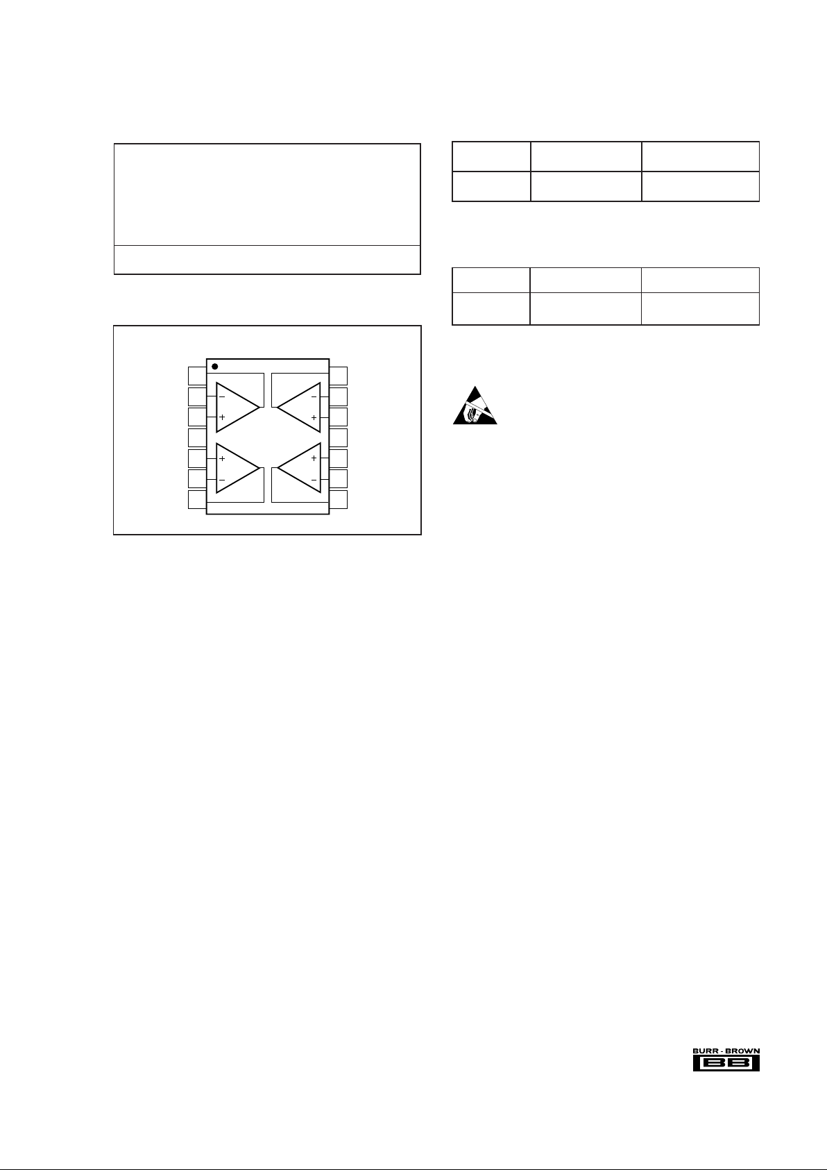
PIN CONFIGURATION
Top View DIP/SO-14
ORDERING INFORMATION
(1)
PRODUCT PACKAGE TEMPERATURE RANGE
OPA4658P 14-Pin Plastic DIP –40°C to +85°C
OPA4658U, UB SO-14 Surface Mount –40°C to +85°C
NOTE: (1) The "B" grade of the SOIC package will be marked with a "B" by pin 8.
Refer to mechanical section for the location.
ELECTROSTATIC
DISCHARGE SENSITIVITY
This integrated circuit can be damaged by ESD. Burr-Brown
recommends that all integrated circuits be handled with
appropriate precautions. Failure to observe proper handling
and installation procedures can cause damage.
ESD damage can range from subtle performance degradation
to complete device failure. Precision integrated circuits may
be more susceptible to damage because very small parametric
changes could cause the device not to meet its published
specifications.
The information provided herein is believed to be reliable; however, BURR-BROWN assumes no responsibility for inaccuracies or omissions. BURR-BROWN assumes
no responsibility for the use of this information, and all use of such information shall be entirely at the user’s own risk. Prices and specifications are subject to change
without notice. No patent rights or licenses to any of the circuits described herein are implied or granted to any third party. BURR-BROWN does not authorize or warrant
any BURR-BROWN product for use in life support devices and/or systems.
Page 4
4
®
OPA4658
TYPICAL PERFORMANCE CURVES
At TA = +25°C, VS = ±5V, RL = 100Ω, CL = 2pF, RFB = 402Ω, unless otherwise noted.
OUTPUT CURRENT vs TEMPERATURE
60
55
50
45
40
–75 –50 –25 0 25 50 75 100 125
Output Current (mA)
Temperature (°C)
IO+
I
O
–
NON-INVERTING INPUT BIAS CURRENT
vs TEMPERATURE
10
8
6
4
2
–75 –50 –25 0 25 50 75 100 125
Non-Inverting Input Bias Current I
B
+ (µA)
Temperature (°C)
OUTPUT SWING vs TEMPERATURE
4
3
2
1
0
–75 –50 –25 0 25 50 75 100 125
Output Swing (V)
Temperature (°C)
±V
O
RL = 250Ω
±V
O
RL = 100Ω
INVERTING INPUT BIAS CURRENT
vs TEMPERATURE
8
6
4
2
0
–75 –50 –25 0 25 50 75 100 125
Inverting Input Bias Current I
B
– (µA)
Temperature (°C)
PSRR AND CMRR vs TEMPERATURE
85
80
75
70
65
60
55
50
45
–75 –50 –25 0 25 50 75 100 125
PSRR , CMRR (dB)
Temperature (°C)
PSRR
PSR+
PSR–
CMRR
SUPPLY CURRENT vs TEMPERATURE
(Total of All Four Op Amps)
21
20
19
18
17
–75 –50 –25 0 25 50 75 100 125
Supply Current (±mA)
Temperature (°C)
Page 5
5
®
OPA4658
TYPICAL PERFORMANCE CURVES (CONT)
At TA = +25°C, VS = ±5V, RL = 100Ω, CL = 2pF, RFB = 402Ω, unless otherwise noted.
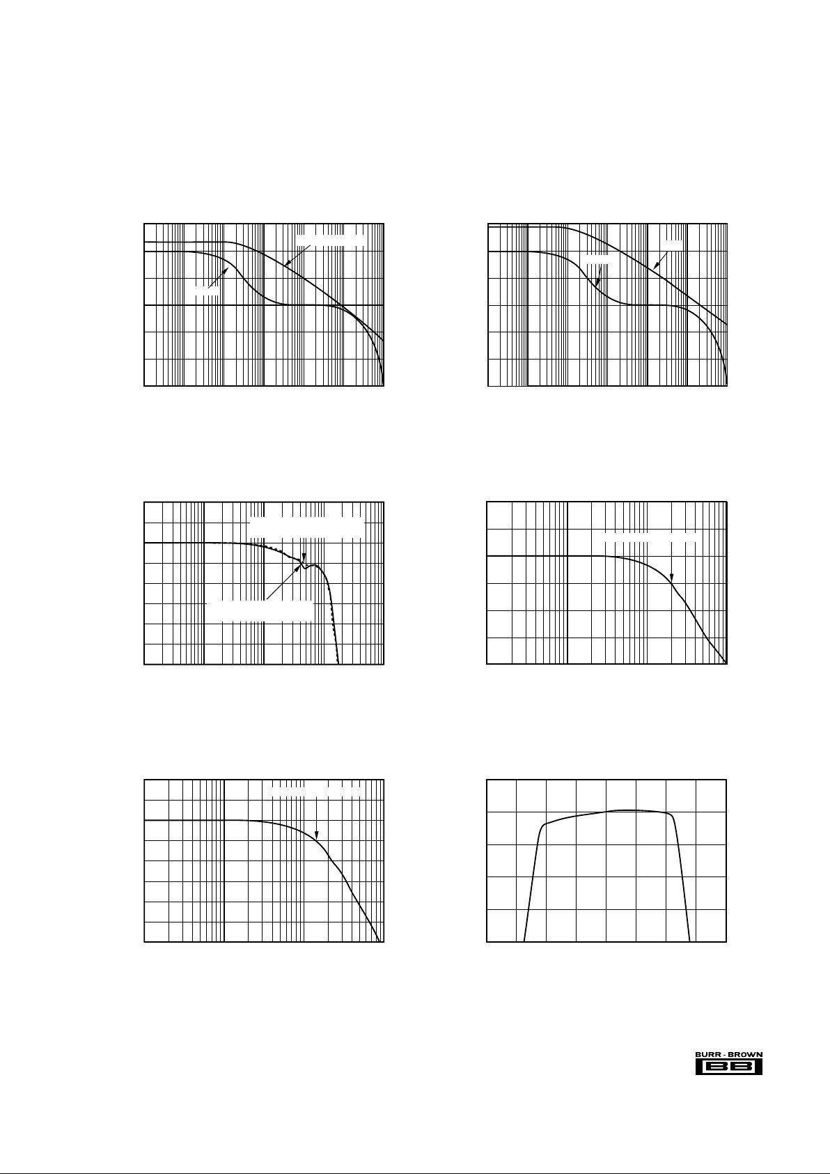
OPEN-LOOP GAIN AND PHASE vs FREQUENCY
Frequency (Hz)
60
40
20
0
–20
–40
–60
0
–45
–90
–135
–180
–225
1k 10k 100k 1M 10M 100M 1G
Open-Loop Gain (dB)
Open-Loop Phase (°)
Gain
Phase
COMMON-MODE REJECTION
vs INPUT COMMON-MODE VOLTAGE
55
50
45
40
35
30
–4–3–2–101234
Common-Mode Rejection (dB)
Common-Mode Voltage (V)
CLOSED-LOOP BANDWIDTH (G = +5)
Frequency (Hz)
20
17
14
11
8
5
2
1M 10M 100M 1G
Bandwidth = 205MHz
Gain (dB)
10
6
10
5
10
4
10
3
10
2
10
1
1
0
–45
–90
–135
–180
–225
1k 10k 100k 1M 10M 100M 1G
OPEN-LOOP TRANSIMPEDANCE AND PHASE
vs FREQUENCY
Frequency (Hz)
Transimpedance (Ω)
Open-Loop Phase (°)
Phase
Transimpedance
CLOSED-LOOP BANDWIDTH (G = +10)
Frequency (Hz)
26
23
20
17
14
11
8
5
2
1M 10M 100M 1G
Gain (dB)
Bandwidth = 134MHz
CLOSED-LOOP BANDWIDTH (G = +2)
Frequency (Hz)
12
9
6
3
0
–3
–6
–9
–12
1M 10M 100M 1G 10G
Gain (dB)
SO-14 Bandwidth = 458MHz
(Dashed Line)
DIP Bandwidth = 435M
(Solid Line)
Page 6

6
®
OPA4658
At TA = +25°C, VS = ±5V, RL = 100Ω, CL = 2pF, RFB = 402Ω, unless otherwise noted.
TYPICAL PERFORMANCE CURVES (CONT)
5MHz HARMONIC DISTORTION vs OUTPUT SWING
(G = +2)
01234
Output Swing (Vp-p)
Harmonic Distortion (dBc)
–50
–60
–70
–80
–90
–100
3f
O
2f
O
10MHz HARMONIC DISTORTION vs OUTPUT SWING
(G = +2)
01234
Output Swing (Vp-p)
Harmonic Distortion (dBc)
–50
–60
–70
–80
–90
–100
3f
O
2f
O
100k 1M 10M 100M
–40
–60
–80
–100
Harmonic Distortion (dBc)
Frequency (Hz)
HARMONIC DISTORTION vs FREQUENCY
(G = +2, V
O
= 2Vp-p)
2f
O
3f
O
SMALL SIGNAL TRANSIENT RESPONSE
(G = +2)
Time (5ns/div)
160
120
80
40
0
–40
–80
–120
–160
Output Voltage (mV)
LARGE SIGNAL TRANSIENT RESPONSE
(G = +2)
Time (5ns/div)
1.6
1.2
0.8
0.4
0
–0.4
–0.8
–1.2
–1.6
Output Voltage (V)
40
35
30
25
20
15
10
10
1009080706050403020
RECOMMENDED ISOLATION RESISTANCE
vs CAPACITIVE LOAD
Capacitive Load (pf)
Isolation Resistance
G = +2
C
L
1kΩ
R
ISO
402Ω
402Ω
Page 7

7
®
OPA4658
TYPICAL PERFORMANCE CURVES (CONT)
At TA = +25°C, VS = ±5V, RL = 100Ω, CL = 2pF, RFB = 402Ω, unless otherwise noted.
HARMONIC DISTORTION vs GAIN
(f
O
= 5MHz, VO = 2Vp-p)
Non-Inverting Gain (V/V)
Harmonic Distortion (dBc)
–50
–55
–60
–65
–70
2345
678910
2f
O
3f
O
–60
–65
–70
–40 –20 0 20 40 60 80 100
Temperature (°C)
HARMONIC DISTORTION vs TEMPERATURE
(G = +2, V
O
= 2Vp-p, fO = 5MHz)
Harmonic Distortion (dBc)
3f
O
2f
O
Page 8

8
®
OPA4658
For non-inverting operation, the input signal is applied to the
non-inverting (high impedance buffer) input. The output
(buffer) error current (IE) is generated at the low impedance
inverting input. The signal generated at the output is fed back
to the inverting input such that the overall gain is (1 + RFB/RFF).
Where a voltage-feedback amplifier has two symmetrical high
impedance inputs, a current feedback amplifier has a low
inverting (buffer output) impedance and a high non-inverting
(buffer input) impedance.
The closed-loop gain for the OPA4658 can be calculated
using the following equations:
(1)
(2)
At higher gains the small value inverting input impedance
causes an apparent loss in bandwidth. This can be seen from
the equation:
(3)
This loss in bandwidth at high gains can be corrected
without affecting stability by lowering the value of the
feedback resistor from the specified value of 402Ω.
OFFSET VOLTAGE AND NOISE
The output offset is the algebraic sum of the input offset
voltage and bias current errors. The output offset for noninverting operation is calculated by the following equation:
(4)
If all terms are divided by the gain (1 + R
FB/RFF
) it can be
observed that input referred offsets improve as gain increases.
The effective noise at the output can be determined by taking
APPLICATIONS INFORMATION
THEORY OF OPERATION
Conventional op amps depend on feedback to drive their
inputs to the same potential, however the current feedback
op amp’s inverting and non-inverting inputs are connected
by a unity gain buffer, thus enabling the inverting input to
automatically assume the same potential as the non-inverting input. This results in very low impedance at the inverting
input to sense the feedback as an error current signal.
DISCUSSION OF PERFORMANCE
The OPA4658 is a low-power, unity gain stable, current
feedback operational amplifier which operates on ±5V power
supply. The current feedback architecture offers the following important advantages over voltage feedback architectures: (1) the high slew rate allows the large signal performance to approach the small signal performance, and (2)
there is very little bandwidth degradation at higher gain
settings.
The current feedback architecture of the OPA4658 provides
the traditional strength of excellent large signal response
plus wide bandwidth, making it a good choice for use in high
resolution video, medical imaging and DAC I/V Conversion. The low power requirements make it an excellent
choice for numerous portable applications.
DC GAIN TRANSFER CHARACTERISTICS
The circuit in Figure 1 shows the equivalent circuit for
calculating the DC gain. When operating the device in the
inverting mode, the input signal error current (I
E
) is ampli-
fied by the open loop transimpedance gain (T
O
). The output
signal generated is equal to T
O
x IE. Negative feedback is
applied through R
FB
such that the device operates at a gain
equal to –R
FB/RFF
.
FIGURE 1. Equivalent Circuit.
V
O
T
O
C
C
L
SRS
(50Ω)
C
1
V
I
V
N
R
FF
R
FB
I
E
+
–
Inverting Gain =
–
R
FB
R
FF
1 +
1
Loop Gain
Non−Inverting Gain =
1 +
R
FB
R
FF
1 +
1
Loop Gain
whereLoop Gain =
T
O
RFB+ RS1 +
R
FB
R
FF
ƒ
ACTUAL
BW ≈
ƒ
AV=+2
()
BW
[]
x1.25
()
1+
R
S
R
FB
× 1 +
R
FB
R
FF
VIO1 +
R
FB
R
FF
± Ib
I
× R
FB
OutputOffsetVoltage =±IbN× RN1 +
R
F
B
R
FF
±
FIGURE 2. Output Offset Voltage Equivalent Circuit.
R
FB
R
FF
Ib
I
R
N
Ib
N
V
IO
Page 9

9
®
OPA4658
The feedback resistor value acts as the frequency response
compensation element for a current feedback type amplifier.
The 402Ω used in setting the specification achieves a nominal maximally flat butterworth response while assuming a
2pF output pin parasitic. Increasing the feedback resistor
will over compensate the amplifier, rolling off the frequency
response, while decreasing it will decrease phase margin,
peaking up the frequency response.
d) Connections to other wideband devices on the board
may be made with short direct traces or through on-board
transmission lines. For short connections, consider the trace
and the input to the next device as a lumped capacitive load.
Relatively wide traces (50 to 100 mils) should be used,
preferably with ground and power planes opened up around
them. Estimate the total capacitive load and set R
ISO
from
the plot of recommended R
ISO
vs capacitive load. Low
parasitic loads may not need an R
ISO
since the OPA4658 is
nominally compensated to operate with a 2pF parasitic load.
If a long trace is required and the 6dB signal loss intrinsic to
doubly terminated transmission lines is acceptable, implement a matched impedance transmission line using microstrip
or stripline techniques (consult an ECL design handbook for
microstrip and stripline layout techniques). A 50Ω environment is not necessary on board, and in fact a higher impedance environment will improve distortion as shown in the
distortion vs load plot. With a characteristic impedance
defined based on board material and desired trace dimensions, a matching series resistor into the trace from the
output of the amplifier is used as well as a terminating shunt
resistor at the input of the destination device. Remember
also that the terminating impedance will be the parallel
combination of the shunt resistor and the input impedance of
the destination device; the total effective impedance should
match the trace impedance. Multiple destination devices are
best handled as separate transmission lines, each with their
own series and shunt terminations.
If the 6dB attenuation loss of a doubly terminated line is
unacceptable, a long trace can be series-terminated at the
source end only. This will help isolate the line capacitance
from the op amp output, but will not preserve signal integrity
as well as a doubly terminated line. If the shunt impedance
at the destination end is finite, there will be some signal
attenuation due to the voltage divider formed by the series
and shunt impedances.
e) Socketing a high speed part like the OPA4658 is not
recommended. The additional lead length and pin-to-pin
capacitance introduced by the socket creates an extremely
troublesome parasitic network which can make it almost
impossible to achieve a smooth, stable response. Best results
are obtained by soldering the part onto the board. If socketing for the DIP package is desired, high frequency flush
mount pins (e.g., McKenzie Technology #710C) can give
good results.
the root sum of the squares of equation (4) and applying the
spectral noise values found in the Typical Performance Curve
graph section. This applies to noise from the op amp only.
Note that both the noise figure (NF) and the equivalent input
offset voltages improve as the closed loop gain increases (by
keeping R
FB
fixed and reducing RFF with RN = 0Ω).
INCREASING BANDWIDTH AT HIGH GAINS
The closed-loop bandwidth can be extended at high gains by
reducing the value of the feedback resistor R
FB
. This bandwidth reduction is caused by the feedback current being split
between RS and R
FF
(refer to Figure 1). As the gain increases
(for a fixed R
FB
), more feedback current is shunted through
R
FF
, which reduces closed-loop bandwidth.
CIRCUIT LAYOUT AND BASIC OPERATION
Achieving optimum performance with a high frequency amplifier like the OPA4658 requires careful attention to layout
parasitics and selection of external components. Recommendations for PC board layout and component selection include:
a) Minimize parasitic capacitance to any ac ground for all
of the signal I/O pins. Parasitic capacitance on the output
and inverting input pins can cause instability; on the noninverting input it can react with the source impedance to
cause unintentional bandlimiting. To reduce unwanted capacitance, a window around the signal I/O pins should be
opened in all of the ground and power planes. Otherwise,
ground and power planes should be unbroken elsewhere on
the board.
b) Minimize the distance (< 0.25") from the two power pins
to high frequency 0.1µF decoupling capacitors. At the pins,
the ground and power plane layout should not be in close
proximity to the signal I/O pins. Avoid narrow power and
ground traces to minimize inductance between the pins and
the decoupling capacitors. Larger (2.2µF to 6.8µF) decoupling
capacitors, effective at lower frequencies, should also be
used. These may be placed somewhat farther from the
device and may be shared among several devices in the same
area of the PC board.
c) Careful selection and placement of external components will preserve the high frequency performance of the
OPA4658. Resistors should be a very low reactance type.
Surface mount resistors work best and allow a tighter overall
layout. Metal film or carbon composition axially-leaded
resistors can also provide good high frequency performance.
Again, keep their leads as short as possible. Never use
wirewound type resistors in a high frequency application.
Since the output pin and the inverting input pin are most
sensitive to parasitic capacitance, always position the feedback and series output resistor, if any, as close as possible to
the package pins. Other network components, such as noninverting input termination resistors, should also be placed
close to the package.
Page 10

10
®
OPA4658
ESD PROTECTION
ESD damage has been well recognized for MOSFET devices, but any semiconductor device is vulnerable to this
potentially damaging source. This is particularly true for
very high speed, fine geometry processes.
ESD damage can cause subtle changes in amplifier input
characteristics without necessarily destroying the device. In
precision operational amplifiers, this may cause a noticeable
degradation of offset voltage and drift. Therefore, ESD
handling precautions are strongly recommended when handling the OPA4658.
OUTPUT DRIVE CAPABILITY
The OPA4658 has been optimized to drive 75Ω and 100Ω
resistive loads. The device can drive 2Vp-p into a 75Ω load.
This high-output drive capability makes the OPA4658 an
ideal choice for a wide range of RF, IF, and video applications. In many cases, additional buffer amplifiers are unneeded.
Many demanding high-speed applications such as
ADC/DAC buffers require op amps with low wideband
output impedance. For example, low output impedance is
essential when driving the signal-dependent capacitances at
the inputs of flash A/D converters. As shown in Figure 3, the
OPA4658 maintains very low closed-loop output impedance
over frequency. Closed-loop output impedance increases
with frequency since loop gain is decreasing with frequency.
max = (±VS)2 /4RL. Note that it is the voltage across the
output transistor, and not the load, that determines the power
dissipated in the output stage.
The short-circuit condition represents the maximum amount
of internal power dissipation that can be generated. The
variation of output current with temperature is shown in the
Typical Performance Curves.
CAPACITIVE LOADS
The OPA4658’s output stage has been optimized to drive
low resistive loads. Capacitive loads, however, will decrease
the amplifier’s phase margin which may cause high frequency peaking or oscillations. Capacitive loads greater than
5pF should be buffered by connecting a small resistance,
usually 5Ω to 25Ω, in series with the output as shown in
Figure 4. This is particularly important when driving high
capacitance loads such as flash A/D converters.
In general, capacitive loads should be minimized for optimum high frequency performance. Coax lines can be driven
if the cable is properly terminated. The capacitance of coax
cable (29pF/foot for RG-58) will not load the amplifier
when the coaxial cable or transmission line is terminated
with its characteristic impedance.
FIGURE 3. Closed-Loop Output Impedance vs Frequency.
100
10
1
0.1
0.01
0.001
10k 100k
1M
10M
100M
Output Impedance (Ω)
Frequency (Hz)
G = +2
THERMAL CONSIDERATIONS
The OPA4658 does not require a heat sink for operation in
most environments. At extreme temperatures and under full
load conditions a heat sink may be necessary.
The internal power dissipation is given by the equation
P
D
= P
DQ
+ PDL, where PDQ is the quiescent power dissipa-
tion and P
DL
is the power dissipation in the output stage due
to the load. (For ±V
S
= ±5V, P
DQ
= 10V x 34mA = 340mW,
max). For the case where the amplifier is driving a grounded
load (RL) with a DC voltage (±V
OUT
) the maximum value of
P
DL
occurs at ±V
OUT
= ±VS/2, and is equal to PDL,
OPA4658
C
L
R
L
50Ω
R
S
(R
S
typically 5Ω to 25Ω)
402Ω402Ω
1/4
COMPENSATION
The OPA4658 is internally compensated and is stable in
gains of two or greater, with a phase margin of approximately 66° in a gain of +2V/V. (Note that, from a stability
standpoint, an inverting gain of –1V/V is equivalent to a
noise gain of 2.) Gain and phase response for other gains are
shown in the Typical Performance Curves.
The high-frequency response of the OPA4658 in a good
layout is very flat with frequency.
DISTORTION
The OPA4658’s Harmonic Distortion characteristics into a
100Ω load are shown vs frequency and power output in the
Typical Performance Curves. Distortion can be further improved by increasing the load resistance as illustrated in
Figure 5. Remember to include the contribution of the
feedback resistance when calculating the effective load resistance seen by the amplifier.
FIGURE 4. Driving Capacitive Loads.
Page 11

11
®
OPA4658
–50
–60
–70
–80
–90
–100
Load Resistance (Ω)
Harmonic Distortion (dBc)
10 100 1k
2f
O
3f
O
G = +2
The third-order intercept is an important parameter for many
RF amplifier applications. Figure 6 shows the OPA4658’s
two tone, third-order intercept vs frequency. This curve is
particularly useful for determining the magnitude of the
third harmonic as a function of frequency, load resistance,
and gain. For example, assume that the application requires
the OPA4658 to operate in a gain of +2V/V and drive
2Vp-p into 100Ω at a frequency of 10MHz. Referring to
Figure 6 we find that the intercept point is +38dBm. The
magnitude of the third harmonic can now be easily calculated from the expression:
Third Harmonic (dBc) = 2(OPI
3
P – PO)
where OPI
3
P = third-order output intercept, dBm
P
O
= output level, dBm
For this case OPI
3
P = 38dBm, PO = 7dBm, and the third
Harmonic = 2(38 – 7) = 62dB below the fundamental. The
OPA4658’s low distortion makes the device an excellent
choice for a variety of RF signal processing applications.
CROSSTALK
Crosstalk is the undesired result of the signal of one channel
mixing with and reproducing itself in the output of another
channel or channels. Crosstalk is inclined to occur in most
multichannel integrated circuits. In quad devices, the effect of
crosstalk is measured by driving three channels and observing
the output of the undriven channel over various frequencies.
The magnitude of this effect is referenced in terms of channelto-channel isolation and expressed in decibels. Input referred
points to the fact that there is a direct correlation between gain
and crosstalk, therefore at increased gain, crosstalk also increases by a factor equal to that of the gain. Figure 7 illustrates
the measured effect of crosstalk in the OPA4658U.
FIGURE 5. 5MHz Harmonic Distortion vs Load Resistance.
FIGURE 6. Third Order Intercept Point vs Frequency.
70
60
50
40
30
20
100k 1M 10M 100M
Third Order Intercept Point (dBm)
Frequency (Hz)
G = +2
(G = +2, R
L
= 100Ω, RFB = 402Ω)
FIGURE 8. Configuration for Testing Differential Gain/Phase.
OPA4658
75Ω
75Ω
402Ω
402Ω
75Ω
75Ω
TEK TSG 130A
TEK VM700A
1/4
DIFFERENTIAL GAIN AND PHASE
Differential Gain (DG) and Differential Phase (DP) are critical specifications for video applications. DG is defined as the
percent change in closed-loop gain over a specified change in
output voltage level. DP is defined as the change in degrees of
the closed-loop phase over the same output voltage change.
Both DG and DP are specified at the NTSC sub-carrier
frequency of 3.58MHz and the PAL subcarrier of 4.43MHz.
All NTSC measurements were performed using a Tektronix
model VM700A Video Measurement Set.
DG and DP of the OPA4658 were measured with the amplifier
in a gain of +2V/V with 75Ω input impedance and the output
back-terminated in 75Ω. The input signal selected from the
generator was a 0V to 1.4V modulated ramp with sync pulse.
With these conditions the test circuit shown in Figure 8
delivered a 100IRE modulated ramp to the 75Ω input of the
video analyzer. The signal averaging feature of the analyzer
FIGURE 7. Channel-to-Channel Isolation (three active channels).
Frequency (Hz)
10
0
–10
–20
–30
–40
–50
–60
–70
–80
–90
1M 10M 100M
Isolation (dB)
G = +2
Page 12

12
®
OPA4658
FIGURE 9. Noise Figure vs Source Resistance.
10 100 1k 10k 100k
40
30
20
10
0
Noise Figure (dB)
Source Resistance (Ω)
NF = 10LOG 1 +
e
n
2
+ (InRs)
2
4KTR
S
TYPICAL APPLICATIONS
FIGURE 10. Low Distortion Video Amplifier.
OPA4658
V
OUT
402Ω402Ω
Video
Input
75Ω
75Ω
75Ω Transmission Line
75Ω
1/4
was used to establish a reference against which the performance of the amplifier was measured. Signal averaging was
also used to measure the DG and DP of the test signal in order
to eliminate the generator’s contribution to measured amplifier performance. Typical performance of the OPA4658 is
0.015% differential gain and 0.02° differential phase to both
NTSC and PAL standards.
NOISE FIGURE
The OPA4658’s voltage and current noise spectral densities
are specified in the Typical Performance Curves. For RF
applications, however, Noise Figure (NF) is often the preferred noise specification since it allows system noise performance to be more easily calculated. The OPA4658’s
Noise Figure vs Source Resistance is shown in Figure 9.
SPICE MODELS
Computer simulation using SPICE is often useful when
analyzing the performance of analog circuits and systems.
This is particularly true for Video and RF amplifier circuits
where parasitic capacitance and inductance can have a major
effect on circuit performance. SPICE models using MicroSim
Corporation’s PSpice are available for the OPA4658. Evaluation PC boards are also available. Contract Burr-Brown
applications departments to receive a SPICE Diskette.
DEMONSTRATION BOARD PACKAGE PRODUCT
DEM-OPA465xP 8-Pin DIP OPA4658P
DEM-OPA465xU SO-8 OPA4658U
OPA4658UB
Page 13

13
®
OPA4658
FIGURE 11. Circuit Detail for the PC Board Layout of Figure 12.
R
23
R
28
Out
D
J
12
1
2
GND
–5V
P2
R
24
R
22
+In
D
R
26
R
31
R
27
R
25
–In
D
J
10
J
11
13
11
14
12
C30.1µF
C42.2µF
R
20
R
15
OPA4658
OPA4658
Out
C
J
7
R
21
R
19
+In
C
R
17
R
18
R
32
R
16
–In
C
J
9
J
8
9
4
8
10
C22.2µF
C10.1µF
C
7
C
8
1/4
1/4
1
2
GND
+5V
P1
R
6
R
1
Out
A
J
1
R
7
R
5
+In
A
R
3
R
4
R
29
R
5
–In
A
J
3
J
2
213
OPA4658
C
5
1/4
R
9
R
14
Out
B
J
6
R
10
R
8
+In
B
R
12
R
13
R
30
R
11
–In
B
J
4
J
5
675
OPA4658
C
6
1/4
U1
OPA465xP
Page 14

14
®
OPA4658
DEM-OPA465xP Demonstration Board Layout
(A) (B)
FIGURE 12a. Board Silkscreen (Bottom). 12b. Board Silkscreen (Top). 12c. Board Layout (Solder Side). 12d. Board Layout
(Component Side).
(C)
(D)
 Loading...