

Datasheet OPA2353EA-250, OPA2353EA-2K5, OPA2353UA-2K5, OPA2353UA, OPA353UA Datasheet (Burr Brown)
...Page 1
®
O
OPA2353
P
A4353
OPA4353
OPA353
OPA2353
For most current data sheet and other product
information, visit www.burr-brown.com
High-Speed, Single-Supply, Rail-to-Rail
OPERA TIONAL AMPLIFIERS
Micro
FEATURES
● RAIL-TO-RAIL INPUT
● RAIL-TO-RAIL OUTPUT (within 10mV)
● WIDE BANDWIDTH: 44MHz
● HIGH SLEW RATE: 22V/µs
● LOW NOISE: 5nV/√Hz
● LOW THD+NOISE: 0.0006%
● UNITY-GAIN STABLE
●
Micro
SIZE PACKAGES
● SINGLE, DUAL, AND QUAD
DESCRIPTION
OPA353 series rail-to-rail CMOS operational amplifiers are designed for low cost, miniature applications.
They are optimized for low voltage, single-supply operation. Rail-to-rail input/output, low noise (5nV/√Hz),
and high speed operation (44MHz, 22V/µs) make them
ideal for driving sampling analog-to-digital converters.
They are also well suited for cell phone PA control
loops and video processing (75Ω drive capability) as
well as audio and general purpose applications. Single,
dual, and quad versions have identical specifications
for design flexibility.
The OPA353 series operates on a single supply as low as
2.5V with an input common-mode voltage range that
SPICE Model available at www.burr-brown.com
Amplifier
OPA4353
™
Series
APPLICATIONS
● CELL PHONE PA CONTROL LOOPS
● DRIVING A/D CONVERTERS
● VIDEO PROCESSING
● DATA ACQUISITION
● PROCESS CONTROL
● AUDIO PROCESSING
● COMMUNICATIONS
● ACTIVE FILTERS
● TEST EQUIPMENT
extends 300mV beyond the supply rails. Output voltage
swing is to within 10mV of the supply rails with a 10kΩ
load. Dual and quad designs feature completely independent circuitry for lowest crosstalk and freedom from
interaction.
The single (OPA353) packages are the tiny 5-lead SOT23-5 surface mount and SO-8 surface mount. The dual
(OPA2353) comes in the miniature MSOP-8 surface
mount and SO-8 surface mount. The quad (OPA4353)
packages are the space-saving SSOP-16 surface mount
and SO-14 surface mount. All are specified from –40°C
to +85°C and operate from –55°C to +125°C.
OPA4353
OPA353
NC
1
–In
2
+In
3
V–
OPA353
Out
1
V–
2
+In
3
SOT-23-5
International Airport Industrial Park • Mailing Address: PO Box 11400, Tucson, AZ 85734 • Street Address: 6730 S. Tucson Blvd., Tucson, AZ 85706 • Tel: (520) 746-1111
Twx: 910-952-1111 • Internet: http://www.burr-brown.com/ • Cable: BBRCORP • Telex: 066-6491 • FAX: (520) 889-1510 • Immediate Product Info: (800) 548-6132
© 1998 Burr-Brown Corporation PDS-1479B Printed in U.S.A. March, 1999
4
V+
5
–In
4
SO-8
NC
8
V+
7
Output
6
NC
5
Out A
–In A
+In A
V–
1
2
3
4
SO-8, MSOP-8
OPA2353
A
8
7
B
6
5
V+
Out B
–In B
+In B
Out A
–In A
+In A
+V
+In B
–In B
Out B
NC
1
2
AD
3
4
5
BC
6
7
8
SSOP-16
(SO-14 package not shown)
Out D
16
–In D
15
+In D
14
–V
13
+In C
12
–In C
11
Out C
10
NC
9
Page 2
SPECIFICATIONS: VS = 2.7V to 5.5V
At TA = +25°C, RL = 1kΩ connected to VS/ 2 and V
Boldface limits apply over the specified temperature range, T
PARAMETER CONDITION MIN TYP
OFFSET VOLTAGE
Input Offset Voltage V
= –40°C to +85°C ±10 mV
T
A
vs Temperature T
vs Power Supply Rejection Ratio PSRR V
= –40°C to +85°C VS = 2.7V to 5.5V, VCM = 0V 175 µV/V
T
A
Channel Separation (dual, quad) dc 0.15 µV/V
INPUT BIAS CURRENT
Input Bias Current I
T
= –40°C to +85°C See Typical Curve
A
Input Offset Current I
NOISE
Input Voltage Noise, f = 100Hz to 400kHz 4 µVrms
Input Voltage Noise Density, f = 10kHz e
f = 100kHz 5 nV/√Hz
Current Noise Density, f = 10kHz i
INPUT VOLTAGE RANGE
Common-Mode Voltage Range V
Common-Mode Rejection Ratio CMRR –0.1V < V
= –40°C to +85°C VS = 5V, –0.1V < V
T
A
INPUT IMPEDANCE
Differential 10
Common-Mode 10
OPEN-LOOP GAIN
Open-Loop Voltage Gain A
= –40°C to +85°C RL = 10kΩ, 50mV < VO < (V+) – 50mV 100 dB
T
A
= –40°C to +85°C RL = 1kΩ, 200mV < VO < (V+) – 200mV 100 dB
T
A
FREQUENCY RESPONSE C
Gain-Bandwidth Product GBW G = 1 44 MHz
Slew Rate SR G = 1 22 V/ µs
Settling Time, 0.1% G = ±1, 2V Step 0.22 µs
0.01% G = ±1, 2V Step 0.5 µs
Overload Recovery Time V
Total Harmonic Distortion + Noise THD+N
Differential Gain Error G = 2, R
Differential Phase Error G = 2, R
OUTPUT
Voltage Output Swing from Rail
= –40°C to +85°C RL = 10kΩ, AOL ≥ 100dB 50 mV
T
A
= –40°C to +85°C RL = 1kΩ, A
T
A
Output Current I
Short-Circuit Current I
Capacitive Load Drive C
(4)
V
LOAD
OUT
OUT
POWER SUPPLY
Operating Voltage Range V
Minimum Operating Voltage 2.5 V
Quiescent Current (per amplifier) I
= –40°C to +85°C IO = 0 9 mA
T
A
TEMPERATURE RANGE
Specified Range –40 +85 °C
Operating Range –55 +125 °C
Storage Range –55 +125 °C
Thermal Resistance
SOT-23-5 200 °C/W
MSOP-8 Surface Mount 150 °C/W
SO-8 Surface Mount 150 °C/W
SSOP-16 Surface Mount 100 °C/W
SO-14 Surface Mount 100 °C/W
NOTES: (1) V
the output and power supply rails. (5) See typical performance curve, “Output Voltage Swing vs Output Swing.”
= +5V. (2) V
S
= 0.25V to 2.75V. (3) NTSC signal generator used. See Figure 6 for test circuit. (4) Output voltage swings are measured between
OUT
= VS/ 2, unless otherwise noted.
OUT
= –40°C to +85°C. VS = 5V.
A
OPA353NA, UA
OPA2353EA, UA
OPA4353EA, UA
(1)
OS
B
OS
n
n
CM
V
RL = 10kΩ, 50mV < VO < (V+) – 50mV 100 122 dB
OL
= 1kΩ, 200mV < VO < (V+) – 200mV 100 120 dB
R
L
RL = 600Ω, VO = 2.5Vp-p
VS = 5V ±3 ±8mV
= –40°C to +85°C ±5 µV/°C
A
= 2.7V to 5.5V, VCM = 0V 40 150 µV/V
S
±0.5 ±10 pA
±0.5 ±10 pA
7 nV/√Hz
4 fA/√Hz
–0.1 (V+) + 0.1 V
< (V+) – 2.4V 76 86 dB
CM
= 5V, –0.1V < V
S
= 100pF
L
• G = V
IN
= 600Ω, VO = 1.4V
L
= 600Ω, VO = 1.4V
L
< 5.1V 60 74 dB
CM
< 5.1V 58 dB
CM
13
|| 2.5 Ω || pF
13
|| 6.5 Ω || pF
S
(2)
, G = 1, f = 1kHz
(3)
(3)
0.1 µs
0.0006 %
0.17 %
0.17 deg
MAX UNITS
RL = 10kΩ, AOL ≥ 100dB 10 50 mV
= 1kΩ, AOL ≥ 100dB 25 200 mV
R
L
SC
S
Q
θ
JA
TA = –40°C to +85°C 2.7 5.5 V
≥ 100dB 200 mV
OL
±40
(5)
±80 mA
See Typical Curve
IO = 0 5.2 8 mA
mA
®
OPA353, 2353, 4353
2
Page 3
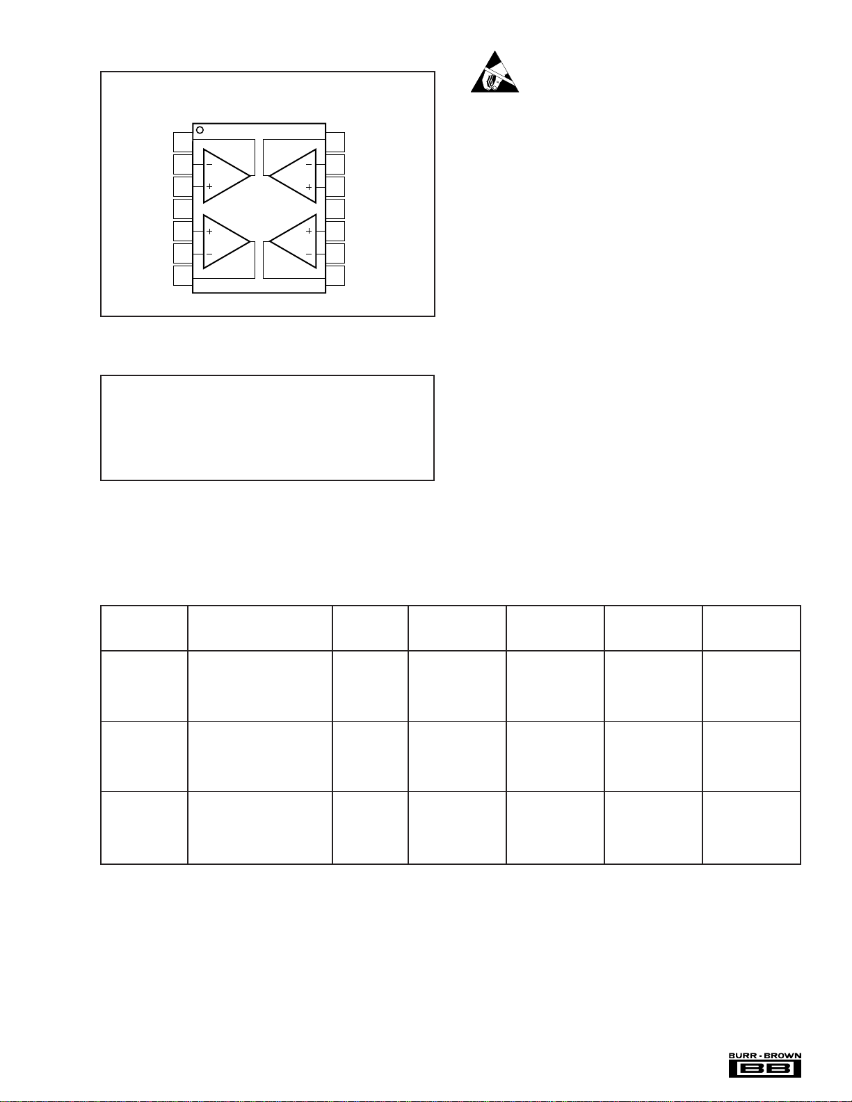
PIN CONFIGURATION
Top View SO-14
OPA4353
Out A
–In A
+In A
V+
+In B
–In B
Out B
1
2
3
4
5
6
7
AD
BC
Out D
14
–In D
13
+In D
12
V–
11
+In C
10
–In C
9
Out C
8
ELECTROSTATIC
DISCHARGE SENSITIVITY
This integrated circuit can be damaged by ESD. Burr-Brown
recommends that all integrated circuits be handled with
appropriate precautions. Failure to observe proper handling
and installation procedures can cause damage.
ESD damage can range from subtle performance degradation to complete device failure. Precision integrated circuits
may be more susceptible to damage because very small
parametric changes could cause the device not to meet its
published specifications.
ABSOLUTE MAXIMUM RATINGS
Supply Voltage ................................................................................... 5.5V
Signal Input Terminals, Voltage
Output Short-Circuit
Operating Temperature ..................................................–55 °C to +125°C
Storage Temperature ..................................................... –55°C to +125°C
Junction Temperature ...................................................................... 150°C
Lead Temperature (soldering, 10s) ................................................. 300°C
NOTES: (1) Stresses above these ratings may cause permanent damage.
Exposure to absolute maximum conditions for extended periods may degrade device reliability. (2) Input terminals are diode-clamped to the power
supply rails. Input signals that can swing more than 0.3V beyond the supply
rails should be current-limited to 10mA or less. (3) Short circuit to ground,
one amplifier per package.
(3)
(2)
.................. (V–) – 0.3V to (V+) + 0.3V
(2)
Current
.............................................................. Continuous
.................................................... 10mA
(1)
PACKAGE/ORDERING INFORMATION
PACKAGE SPECIFIED
PRODUCT PACKAGE NUMBER
DRAWING TEMPERATURE PACKAGE ORDERING TRANSPORT
Single
OPA353NA 5-Lead SOT-23-5 331 –40°C to +85°C D53 OPA353NA/250 Tape and Reel
"""""OPA353NA /3K Tape and Reel
OPA353UA SO-8 Surface Mount 182 –40°C to +85°C OPA353UA OPA353UA Rails
"""""OPA353UA /2K5 Tape and Reel
Dual
OPA2353EA MSOP-8 Surface Mount 337 –40°C to +85°C E53 OPA2353EA /250 Tape and Reel
"""""OPA2353EA/2K5 Tape and Reel
OPA2353UA SO-8 Surface Mount 182 –40 °C to +85°C OPA2353UA OPA2353UA Rails
"""""OPA2353UA/2K5 Tape and Reel
Quad
OPA4353EA SSOP-16 Surface Mount 322 –40°C to +85°C OPA4353EA OPA4353EA /250 Tape and Reel
"""""OPA4353EA /2K5 Tape and Reel
OPA4353UA SO-14 Surface Mount 235 –40°C to +85°C OPA4353UA OPA4353UA Rails
"""""OPA4353UA/2K5 Tape and Reel
NOTES: (1) For detailed drawing and dimension table, please see end of data sheet, or Appendix C of Burr-Brown IC Data Book. (2) Models with a slash (/) are
available only in Tape and Reel in the quantities indicated (e.g., /2K5 indicates 2500 devices per reel). Ordering 2500 pieces of “OPA2353EA/2K5” will get a single
2500-piece Tape and Reel. For detailed Tape and Reel mechanical information, refer to Appendix B of Burr-Brown IC Data Book.
(1)
RANGE MARKING NUMBER
(2)
MEDIA
The information provided herein is believed to be reliable; however, BURR-BROWN assumes no responsibility for inaccuracies or omissions. BURR-BROWN assumes no responsibility
for the use of this information, and all use of such information shall be entirely at the user’s own risk. Prices and specifications are subject to change without notice. No patent rights or
licenses to any of the circuits described herein are implied or granted to any third party. BURR-BROWN does not authorize or warrant any BURR-BROWN product for use in life support
devices and/or systems.
®
3
OPA353, 2353, 4353
Page 4
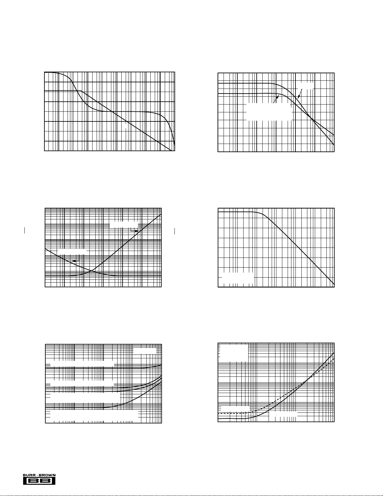
TYPICAL PERFORMANCE CURVES
At TA = +25°C, VS = +5V, and RL = 1kΩ connected to VS/2, unless otherwise noted.
160
140
120
100
80
60
Voltage Gain (dB)
40
20
0
0.1 1
100k
10k
1k
100
Voltage Noise (nV√Hz)
10
1
10 100 1k 10k 100k 1M 10M
OPEN-LOOP GAIN/PHASE vs FREQUENCY
G
10 100 1k 10k 100k 1M 10M 100M
Frequency (Hz)
INPUT VOLTAGE AND CURRENT NOISE
SPECTRAL DENSITY vs FREQUENCY
Current Noise
Voltage Noise
Frequency (Hz)
POWER SUPPLY AND COMMON-MODE
0
–45
φ
10k
1k
100
10
1
0.1
–90
–135
–180
Current Noise (fA√Hz)
100
90
80
70
60
50
Phase (°)
40
30
PSRR, CMRR (dB)
20
10
0
10 100 1k 10k 100k 1M 10M
140
130
120
110
100
90
80
Channel Separation (dB)
70
60
REJECTION RATIO vs FREQUENCY
PSRR
CMRR
(V
= +5V
S
V
= –0.1V to 5.1V)
CM
Frequency (Hz)
CHANNEL SEPARATION vs FREQUENCY
Dual and Quad
Versions
10010 1k 1M100k10k 10M
Frequency (Hz)
TOTAL HARMONIC DISTORTION + NOISE
1
G = 100, 3Vp-p (VO = 1V to 4V)
0.1
0.01
THD+N (%)
0.001
0.0001
G = 10, 3Vp-p (VO = 1V to 4V)
G = 1, 3Vp-p (VO = 1V to 4V)
Input goes through transition region
G = 1, 2.5Vp-p (VO = 0.25V to 2.75V)
Input does NOT go through transition region
10 100 1k 10k 100k
®
vs FREQUENCY
Frequency (Hz)
OPA353, 2353, 4353
RL = 600Ω
(–40dBc)
0.1
(–60dBc)
0.01
(–80dBc)
0.001
Harmonic Distortion (%)
(–100dBc)
0.0001
(–120dBc)
4
HARMONIC DISTORTION + NOISE vs FREQUENCY
1
G = 1
= 2.5Vp-p
V
O
= 600Ω
R
L
3rd Harmonic
1k 10k 100k 1M
2nd Harmonic
Frequency (Hz)
Page 5

TYPICAL PERFORMANCE CURVES (CONT)
QUIESCENT CURRENT vs SUPPLY VOLTAGE
Supply Voltage (V)
Quiescent Current (mA)
6.0
5.5
5.0
4.5
4.0
3.5
3.0
2.0 2.5 3.0 3.5 4.0 4.5 5.0 5.5
Per Amplifier
At TA = +25°C, VS = +5V, and RL = 1kΩ connected to VS/2, unless otherwise noted.
DIFFERENTIAL GAIN/PHASE vs RESISTIVE LOAD
0.5
0.4
0.3
0.2
Differential Gain (%)
Differential Phase (°)
0.1
0
0 100 200 300 500400 600 800700 900 1000
90
80
70
CMRR (dB)
60
50
–75 –50 –25 0 25 50 75 100 125
Phase
Gain
Resistive Load (Ω)
COMMON-MODE AND POWER SUPPLY
REJECTION RATIO vs TEMPERATURE
(V
PSRR
Temperature (°C)
G = 2
V
= 1.4V
O
NTSC Signal Generator
See Figure 6 for test circuit.
CMRR, VS = 5V
= –0.1V to +5.1V)
CM
110
100
90
80
70
PSRR (dB)
130
125
120
115
Open-Loop Gain (dB)
110
–75 –50 –25 0 25 50 75 100 125
40
35
30
25
20
15
Slew Rate (V/µs)
10
5
0
–75 –50 –25 0 25 50 75 100 125
OPEN-LOOP GAIN vs TEMPERATURE
RL = 10kΩ
Temperature (°C)
SLEW RATE vs TEMPERATURE
Negative Slew Rate
Temperature (°C)
RL = 1kΩ
RL = 600Ω
Positive Slew Rate
7.0
6.5
6.0
5.5
5.0
4.5
Quiescent Current (mA)
4.0
3.5
SHORT-CIRCUIT CURRENT vs TEMPERATURE
–75 –50 –25 0 25 50 75 100 125
QUIESCENT CURRENT AND
Temperature (°C)
+I
SC
–I
SC
I
Q
100
90
80
70
60
50
Short-Circuit Current (mA)
40
30
5
®
OPA353, 2353, 4353
Page 6

TYPICAL PERFORMANCE CURVES (CONT)
At TA = +25°C, VS = +5V, and RL = 1kΩ connected to VS/2, unless otherwise noted.
1k
100
10
1
Input Bias Current (pA)
0.1
100
10
1
INPUT BIAS CURRENT vs TEMPERATURE
–75 –50 –25 0 25 50 75 100 125
Temperature (°C)
CLOSED-LOOP OUTPUT IMPEDANCE vs FREQUENCY
INPUT BIAS CURRENT
1.5
1.0
0.5
0.0
Input Bias Current (pA)
–0.5
–0.5 0.0 0.5 1.0 2.01.5 2.5 3.0 3.5 4.0 5.04.5 5.5
6
5
4
vs INPUT COMMON-MODE VOLTAGE
Common-Mode Voltage (V)
MAXIMUM OUTPUT VOLTAGE vs FREQUENCY
VS = 5.5V
Maximum output
voltage without
slew rate-induced
distortion.
0.1
0.01
Output Impedance (Ω)
0.001
0.0001
V+
(V+)–1
(V+)–2
(V–)+2
Output Voltage (V)
(V–)+1
(V–)
G = 100
1 10 100 1k 10k 100k 1M 10M 100M
OUTPUT VOLTAGE SWING vs OUTPUT CURRENT
0 ±10 ±20 ±30 ±40
G = 10
G = 1
Frequency (Hz)
+125°C
Depending on circuit configuration
(including closed-loop gain) performance
may be degraded in shaded region.
+125°C
Output Current (mA)
–55°C
+25°C
+25°C
–55°C
VS = 2.7V
3
2
Output Voltage (Vp-p)
1
0
100k
Frequency (Hz)
OPEN-LOOP GAIN vs OUTPUT VOLTAGE SWING
140
I
= 250µA
OUT
130
120
110
100
90
80
Open-Loop Gain (dB)
70
60
0 20 40 60 10080 120 160140 180 200
Output Voltage Swing from Supply Rails (mV)
I
OUT
I
= 2.5mA
OUT
= 4.2mA
100M1M 10M
®
OPA353, 2353, 4353
6
Page 7

TYPICAL PERFORMANCE CURVES (CONT)
Offset Voltage Drift (µV/°C)
OFFSET VOLTAGE DRIFT
PRODUCTION DISTRIBUTION
35
30
25
20
15
10
5
0
0123456789101112131415
Percent of Amplifiers (%)
Typical production
distribution of
packaged units.
SETTLING TIME vs CLOSED-LOOP GAIN
10
1
0.1
Settling Time (µs)
Closed-Loop Gain (V/V)
±1 ±10 ±100
0.1%
0.01%
At TA = +25°C, VS = +5V, and RL = 1kΩ connected to VS/2, unless otherwise noted.
OFFSET VOLTAGE PRODUCTION DISTRIBUTION
25
Typical production
distribution of
packaged units.
20
15
10
Percent of Units (%)
5
0
–8 –7 –6 –5 4 –3 –2 –1 0 1 2 3 4 5 6 7 8
Offset Voltage (mV)
SMALL-SIGNAL OVERSHOOT vs LOAD CAPACITANCE
80
70
60
50
40
30
Overshoot (%)
20
10
0
10
G = 1
G = –1
G = ±10
1M100 1k 10k 100k
Load Capacitance (pF)
SMALL-SIGNAL STEP RESPONSE
50mV/div
C
100ns/div
= 100pF
L
LARGE-SIGNAL STEP RESPONSE
1V/div
7
OPA353, 2353, 4353
= 100pF
C
L
200ns/div
®
Page 8

APPLICATIONS INFORMATION
OPA353 series op amps are fabricated on a state-of-the-art
0.6 micron CMOS process. They are unity-gain stable and
suitable for a wide range of general purpose applications.
Rail-to-rail input/output make them ideal for driving sampling A/D converters. They are well suited for controlling
the output power in cell phones. These applications often
require high speed and low noise. In addition, the OPA353
series offers a low cost solution for general purpose and
consumer video applications (75Ω drive capability).
Excellent ac performance makes the OPA353 series well
suited for audio applications. Their bandwidth, slew rate,
low noise (5nV/√Hz), low THD (0.0006%), and small package options are ideal for these applications. The class AB
output stage is capable of driving 600Ω loads connected to
any point between V+ and ground.
Rail-to-rail input and output swing significantly increases
dynamic range, especially in low voltage supply applications. Figure 1 shows the input and output waveforms for
VS = +5, G = +1, RL = 1kΩ
5V
V
IN
0
5V
V
OUT
0
FIGURE 1. Rail-to-Rail Input and Output.
1.25V/div
the OPA353 in unity-gain configuration. Operation is
from a single +5V supply with a 1kΩ load connected to
VS/2. The input is a 5Vp-p sinusoid. Output voltage is
approximately 4.95Vp-p.
Power supply pins should be bypassed with 0.01µF ceramic
capacitors.
OPERATING VOLTAGE
OPA353 series op amps are fully specified from +2.7V to
+5.5V. However, supply voltage may range from +2.5V to
+5.5V. Parameters are guaranteed over the specified supply
range—a unique feature of the OPA353 series. In addition,
many specifications apply from –40°C to +85°C. Most
behavior remains virtually unchanged throughout the full
operating voltage range. Parameters which vary significantly with operating voltages or temperature are shown in
the typical performance curves.
RAIL-TO-RAIL INPUT
The guaranteed input common-mode voltage range of the
OPA353 series extends 100mV beyond the supply rails. This
is achieved with a complementary input stage—an
N-channel input differential pair in parallel with a P-channel
differential pair (see Figure 2). The N-channel pair is active
for input voltages close to the positive rail, typically
(V+) – 1.8V to 100mV above the positive supply, while the
P-channel pair is on for inputs from 100mV below the
negative supply to approximately (V+) – 1.8V. There is a
small transition region, typically (V+) – 2V to (V+) – 1.6V, in
which both pairs are on. This 400mV transition region can
vary ±400mV with process variation. Thus, the transition
region (both input stages on) can range from (V+) – 2.4V to
(V+) – 2.0V on the low end, up to (V+) – 1.6V to (V+) – 1.2V
on the high end.
V+
VIN+
V–
(Ground)
FIGURE 2. Simplified Schematic.
®
OPA353, 2353, 4353
Reference
Current
VIN–
V
V
BIAS1
BIAS2
Class AB
Control
Circuitry
V
O
8
Page 9

A double-folded cascode adds the signal from the two input
pairs and presents a differential signal to the class AB output
stage. Normally, input bias current is approximately 500fA.
However, large inputs (greater than 300mV beyond the
supply rails) can turn on the OPA353’s input protection
diodes, causing excessive current to flow in or out of the
input pins. Momentary voltages greater than 300mV beyond
the power supply can be tolerated if the current on the input
pins is limited to 10mA. This is easily accomplished with an
input resistor as shown in Figure 3. Many input signals are
inherently current-limited to less than 10mA, therefore, a
limiting resistor is not required.
FEEDBACK CAPACITOR IMPROVES RESPONSE
For optimum settling time and stability with high-impedance feedback networks, it may be necessary to add a
feedback capacitor across the feedback resistor, RF, as
shown in Figure 4. This capacitor compensates for the zero
created by the feedback network impedance and the
OPA353’s input capacitance (and any parasitic layout
capacitance). The effect becomes more significant with
higher impedance networks.
C
F
V+
I
OVERLOAD
V
IN
10mA max
5kΩ
OPAx353
V
OUT
FIGURE 3. Input Current Protection for Voltages Exceeding
the Supply Voltage.
RAIL-TO-RAIL OUTPUT
A class AB output stage with common-source transistors is
used to achieve rail-to-rail output. For light resistive loads
(>10kΩ), the output voltage swing is typically ten millivolts
from the supply rails. With heavier resistive loads (600Ω to
10kΩ), the output can swing to within a few tens of millivolts from the supply rails and maintain high open-loop
gain. See the typical performance curves “Output Voltage
Swing vs Output Current” and “Open-Loop Gain vs Output
Voltage.”
CAPACITIVE LOAD AND STABILITY
OPA353 series op amps can drive a wide range of capacitive
loads. However, all op amps under certain conditions may
become unstable. Op amp configuration, gain, and load
value are just a few of the factors to consider when determining stability. An op amp in unity gain configuration is the
most susceptible to the effects of capacitive load. The
capacitive load reacts with the op amp’s output impedance,
along with any additional load resistance, to create a pole in
the small-signal response which degrades the phase margin.
In unity gain, OPA353 series op amps perform well with
large capacitive loads. Increasing gain enhances the
amplifier’s ability to drive more capacitance. The typical
performance curve “Small-Signal Overshoot vs Capacitive
Load” shows performance with a 1kΩ resistive load. Increasing load resistance improves capacitive load drive capability.
R
V
IN
R
IN
Where C
capacitance (approximately 9pF) plus any
parastic layout capacitance.
IN
• C
= RF • C
IN
F
is equal to the OPA353’s input
IN
R
V+
C
IN
OPA353
C
IN
F
V
OUT
C
L
FIGURE 4. Feedback Capacitor Improves Dynamic Perfor-
mance.
It is suggested that a variable capacitor be used for the
feedback capacitor since input capacitance may vary between op amps and layout capacitance is difficult to
determine. For the circuit shown in Figure 4, the value of
the variable feedback capacitor should be chosen so that
the input resistance times the input capacitance of the
OPA353 (typically 9pF) plus the estimated parasitic layout
capacitance equals the feedback capacitor times the feedback resistor:
RIN • CIN = RF • C
F
where CIN is equal to the OPA353’s input capacitance
(sum of differential and common-mode) plus the layout
capacitance. The capacitor can be varied until optimum
performance is obtained.
DRIVING A/D CONVERTERS
OPA353 series op amps are optimized for driving medium
speed (up to 500kHz) sampling A/D converters. However,
they also offer excellent performance for higher speed
converters. The OPA353 series provides an effective means
of buffering the A/D’s input capacitance and resulting
charge injection while providing signal gain. For applications requiring high accuracy, the OPA350 series is recommended.
®
9
OPA353, 2353, 4353
Page 10

Figure 5 shows the OPA353 driving an ADS7861. The
ADS7861 is a dual, 12-bit, 500kHz sampling converter in
the small SSOP-24 package. When used with the miniature
package options of the OPA353 series, the combination is
ideal for space-limited and low power applications. For
further information consult the ADS7861 data sheet.
OUTPUT IMPEDANCE
The low frequency open-loop output impedance of the
OPA353’s common-source output stage is approximately
1kΩ. When the op amp is connected with feedback, this
value is reduced significantly by the loop gain of the op
amp. For example, with 122dB of open-loop gain, the
output impedance is reduced in unity-gain to less than
0.001Ω. For each decade rise in the closed-loop gain, the
loop gain is reduced by the same amount which results in
a ten-fold increase in output impedance (see the typical
performance curve, “Output Impedance vs Frequency”).
At higher frequencies, the output impedance will rise as
the open-loop gain of the op amp drops. However, at these
frequencies the output also becomes capacitive due to
parasitic capacitance. This prevents the output impedance
from becoming too high, which can cause stability problems when driving capacitive loads. As mentioned previously, the OPA353 has excellent capacitive load drive
capability for an op amp with its bandwidth.
VIDEO LINE DRIVER
Figure 6 shows a circuit for a single supply, G = 2 composite video line driver. The synchronized outputs of a
composite video line driver extend below ground. As
shown, the input to the op amp should be ac-coupled and
shifted positively to provide adequate signal swing to
account for these negative signals in a single-supply configuration.
The input is terminated with a 75Ω resistor and ac-coupled
with a 47µF capacitor to a voltage divider that provides the
dc bias point to the input. In Figure 6, this point is
approximately (V–) + 1.7V. Setting the optimal bias point
requires some understanding of the nature of composite
video signals. For best performance, one should be careful
to avoid the distortion caused by the transition region of
the OPA353’s complementary input stage. Refer to the
discussion of rail-to-rail input.
C
B1
+5V
24 13
+V
+V
ADS7861
IN
OUT
DGND AGND
112
D
A
Serial Data A
Serial Data B
BUSY
CLOCK
CS
RD
CONVST
A0
M0
M1
23
22
21
20
19
18
17
16
15
14
Serial
Interface
2
3
6
5
9
10
2kΩ
4
1/4
OPA4353
C
B0
2kΩ
1/4
OPA4353
C
A1
2kΩ
1/4
OPA4353
C
A0
2kΩ
0.1µF 0.1µF
2
CH B1+
3
7
8
CH B1–
4
CH B0+
5
CH B0–
6
CH A1+
7
CH A1–
8
CH A0+
9
CH A0–
10
REF
11
REF
2kΩ
V
B1
IN
2kΩ
V
B0
IN
2kΩ
V
A1
IN
2kΩ
V
A0
IN
VIN = 0V to 2.45V for 0V to 4.9V output.
Choose C
OPA4353
11
, CB0, CA1, CA0 to filter high frequency noise.
B1
14
1/4
FIGURE 5. OPA4353 Driving Sampling A/D Converter.
®
OPA353, 2353, 4353
10
Page 11

R
G
1kΩ
C
1
220µF
+5V
R
F
1kΩ
+
0.1µF 10µF
C
0.1µF
4
C
2
R
75Ω
47µF
1
R
5kΩ
2
Video
In
FIGURE 6. Single-Supply Video Line Driver.
+5V
50kΩ
(2.5V)
8
REF1004-2.5
4
+5V
R
5kΩ
3
7
OPA353
4
C
10µF
R
1
100kΩ
3
R
5kΩ
6
4
25kΩ
1/2
OPA2353
+5V (pin 7)
R
G
R
2
C
5
1000µF
25kΩ
R
OUT
R
3
R
100kΩ
Cable
V
OUT
R
L
4
G = 5 +
200kΩ
R
G
1/2
OPA2353
R
10kΩ
V
OUT
L
FIGURE 7. Two Op-Amp Instrumentation Amplifier With Improved High Frequency Common-Mode Rejection.
<1pF (prevents gain peaking)
R
10MΩ
+V
λ
OPA353
FIGURE 8. Transimpedance Amplifier.
C
1
4.7µF
V
O
V
C
1
1830pF
IN
10.5kΩ
C
2
270pF
R
49.9kΩ
1
+2.5V
OPA353
2
–2.5V
+2.5V
FIGURE 10. 10kHz High-Pass Filter.
R
1
2.74kΩ
V
IN
R
2
19.6kΩ
C
1nF
OPA353
2
–2.5V
R
20kΩ
V
OUT
L
R
20kΩ
V
OUT
L
FIGURE 9. 10kHz Low-Pass Filter.
11
®
OPA353, 2353, 4353
 Loading...