

Page 1

INTEGRATED CIRCUITS
DATA SH EET
OM5193H
Disk drive spindle and VCM with
servo controller
Product specification
File under Integrated Circuits, IC11
1998 Nov 02
Page 2

Philips Semiconductors Product specification
Disk drive spindle and VCM with
servo controller
CONTENTS
1 FEATURES
1.1 Servo control
1.2 Motor control
1.2.1 Spindle motor driver
1.2.2 Voice coil motor driver
1.3 Miscellaneous items
2 APPLICATIONS
3 GENERAL DESCRIPTION
3.1 Overview
3.2 Servo controller
3.3 Spindle and voice coil motor
3.4 Safety functions
4 QUICK REFERENCE DATA
5 ORDERING INFORMATION
6 BLOCK DIAGRAMS
7 PINNING
8 FUNCTIONAL DESCRIPTION
8.1 Serial interface
8.2 Commutation and sleep mode
8.3 Commutation control
8.3.1 Blanks, Watchdog and Start-up delays
8.3.2 Comdelim delay
8.4 10-bit ADC with 7 analog inputs
8.4.1 Input channels
8.4.2 Input ranges
8.4.3 Conversion modes
8.4.4 Programming register#0
8.4.5 Converter clock frequency values
8.5 10-bit VCM DAC
8.6 Reference voltage
8.7 Stand-alone op-amps
8.8 Analog switch
8.9 Charge pump voltage
8.10 Spindle driver
8.11 VCM driver
8.12 Park the VCM
8.13 Precharge the VCM
8.14 Brake the motor
8.15 Power-on reset
8.16 Thermal monitor and shutdown
8.17 Power supply isolation
8.17.1 External isolation diode
8.17.2 External power FET
8.18 Thermal behaviour
OM5193H
9 LIMITING VALUES
10 HANDLING
11 THERMAL CHARACTERISTICS
12 CHARACTERISTICS
13 APPLICATION INFORMATION
14 PACKAGE OUTLINE
15 SOLDERING
15.1 Introduction
15.2 Reflow soldering
15.3 Wave soldering
15.4 Repairing soldered joints
16 DEFINITIONS
17 LIFE SUPPORT APPLICATIONS
1998 Nov 02 2
Page 3

Philips Semiconductors Product specification
Disk drive spindle and VCM with
servo controller
1 FEATURES
1.1 Servo control
• 10-bit VCM Digital-to-Analog Converter (DAC)
• 7-channel 10-bit Analog-to-Digital Converter (ADC)
• Programmable spindle commutation control logic
• 3-wire serial interface
• Two stand-alone operational amplifiers (op-amps) with
outputs connected to the ADC
• Analog multiplexer with two inputs used to select VCM
seek mode or track-following mode.
1.2 Motor control
1.2.1 S
• 3-phase output motor driver
• 1.9 A maximum available start-up current
• Total R
• Back ElectroMotive Force (BEMF) processing for
sensorless motor commutation
• Linear current control
• External current sense resistor
• External current control loop compensation
• Adjustable slew rate control
• Short-circuit brake
• Adjustable brake-after-park delay time.
1.2.2 V
• 1.5 A maximum current capability
• Total R
• Linear class AB output with low cross-over distortion
delay
• Precision current control loop with external current
sense resistor
• Programmable seek and track-following mode with
adjustable current loop gain
• External current control loop compensation
• Precharge during brake mode
• 20 kHz current control loop bandwidth
• Parking function
• Adjustable park voltage with limiter.
PINDLE MOTOR DRIVER
= 0.6 Ω (typical) at 25 °C
ds(on)
OICE COIL MOTOR DRIVER
= 0.8 Ω (typical) at 25 °C
ds(on)
OM5193H
1.3 Miscellaneous items
• Precision low voltage 5 and 12 V power monitor with
hysteresis
• Precision internal voltage reference for servo and power
control circuits
• Thermal sense circuit with over-temperature shutdown
sensor
• Internal charge pump voltage generator
• Automatic brake-after-park at power-down, thermal
shutdown or sleep mode
• Sleep mode: low power consumption mode.
2 APPLICATIONS
• 12 V hard disk drive products.
3 GENERAL DESCRIPTION
3.1 Overview
The OM5193H is a combination of a voice coil motor and
a spindle motor driver with embedded servo controller
designed for use in disk drives. Configuration and control
registers are set via a 3-wire serial port running up to
30 MHz to interface commonly to a microcontroller or a
digital signal processor.
The device operates at 5 and 12 V power supplies and
integrates safety functions such as power stages
overvoltage protection, power and temperature monitor,
over-temperature shutdown and dynamic
brake-after-park.
The device is contained in a QFP80 package with 18 pins
connected to the leadframe thus providing low thermal
resistance.
3.2 Servo controller
The servo controller includes the following circuits:
• 3-wire serial interface
• Spindle commutation logic
• A 10-bit ADC with 7 inputs selected by an internal
multiplexer
• A 10-bit VCM DAC with 1.5, 2.5 and 3.5 V voltage
references
• Two low-offset stand-alone op-amps
• Analog multiplexer with 2 inputs.
1998 Nov 02 3
Page 4

Philips Semiconductors Product specification
Disk drive spindle and VCM with
servo controller
The serial interface is used:
• To adjust the timing parameters for proper spindle
commutation sequence
• To accurately adjust head positioning via the 10-bit VCM
DAC
• To set VCM seek or track-following mode via the
low-impedance switch
• To select and process analog signals via a 7-channel
multiplexer connected to the 10-bit ADC.
The spindle commutation logic circuit ensures proper
spindle start-up (no reverse rotation) and commutation
sequence for the spindle driver by processing BEMF
sensing circuit output signals.
The two stand-alone op-amps, with the inputs connected
to the read channel IC, provide servo track signals
processed by the microcontroller to perform accurate
track-following mode.
3.3 Spindle and voice coil motor
OM5193H
3.4 Safety functions
The OM5193H is protected against transient voltage
spikes that are generated by the inductive loads of spindle
and VCM.
Power supplies and temperature are monitored in order to
guarantee data reliability and self-protection of the device
in case of power loss or temperatures beyond maximum
rating.
Park and brake functions secure heads and disk media in
case of power-down or high temperature failure. This
function is also activated by the sleep mode.
An internal temperature monitor is available to monitor the
chip temperature and thus prevents over-temperature
shutdown. Internally connected to the ADC channel 4, it
can be used by the microcontroller as an early
‘temperature-too-high’ warning during a long VCM seek
sequence.
The OM5193H drives a 3-phase brushless, sensorless DC
spindle motor and a voice coil motor.
Spindle and voice coil motor power stages with low R
and high current capability are suitable for mid-end and
low-end 12 V disk drives. Power stages are designed in
such a way that external Schottky diodes are not needed.
Spindle current is sensed by an external resistor and
monitored by the external signal SPCC (SPindle Current
Control). Spindle speed is regulated by the microcontroller
via the ZCROSS signal (Zero CROSSing detection
frequency output). BEMF comparators provide the digital
zero crossing signals. These are processed by the
commutation logic circuit to properly switch-on and
switch-off spindle power drivers thus ensuring the rotation
of the motor.
The control of the heads positioning is accomplished by
the internal 10-bit VCM DAC. Seek and track-following
VCM current loop gain is set by external resistors. VCM
zero current is referenced to the 2.5 V internal voltage
reference.
An internal precharge of the actuator (magnetic latch)
during brake mode guarantees total control of the current
when VCM starts running without current spikes.
ds(on)
1998 Nov 02 4
Page 5

Philips Semiconductors Product specification
Disk drive spindle and VCM with
OM5193H
servo controller
4 QUICK REFERENCE DATA
SYMBOL PARAMETER MIN. TYP. MAX. UNIT
Supply voltage
V
DDA1
V
DDD
V
DDA2
Drivers
I
SPOUT
I
VCMRUN
5 ORDERING INFORMATION
TYPE
NUMBER
OM5193H QFP80 plastic quad flat package; 80 leads (lead length 1.95 mm);
5 V analog supply voltage 4.5 5.0 5.5 V
5 V digital supply voltage 4.5 5.0 5.5 V
12 V analog supply voltage 10.8 12.0 13.2 V
spindle start-up current −−1.9 A
VCM current −−1.5 A
PACKAGE
NAME DESCRIPTION VERSION
SOT318-2
body 14 × 20 × 2.8 mm
1998 Nov 02 5
Page 6
Philips Semiconductors Product specification
Disk drive spindle and VCM with
OM5193H
servo controller
6 BLOCK DIAGRAMS
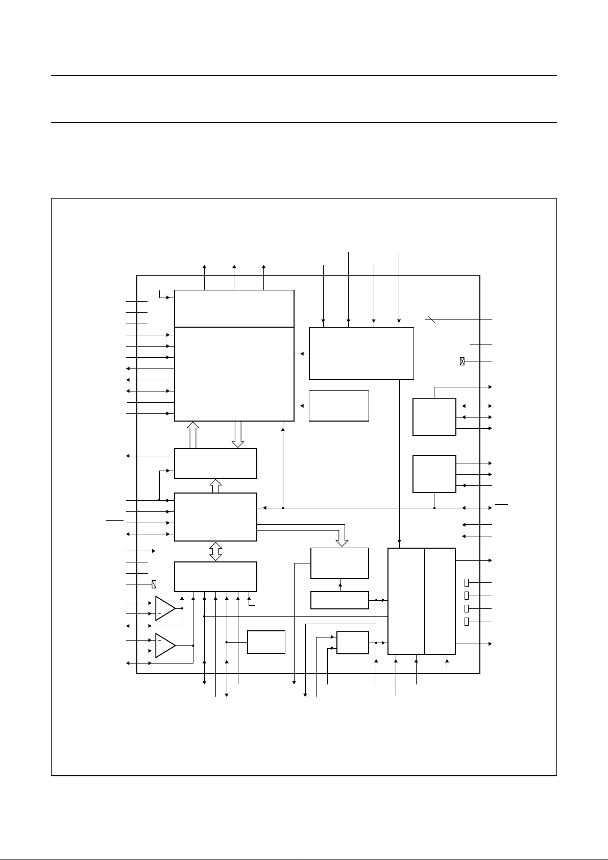
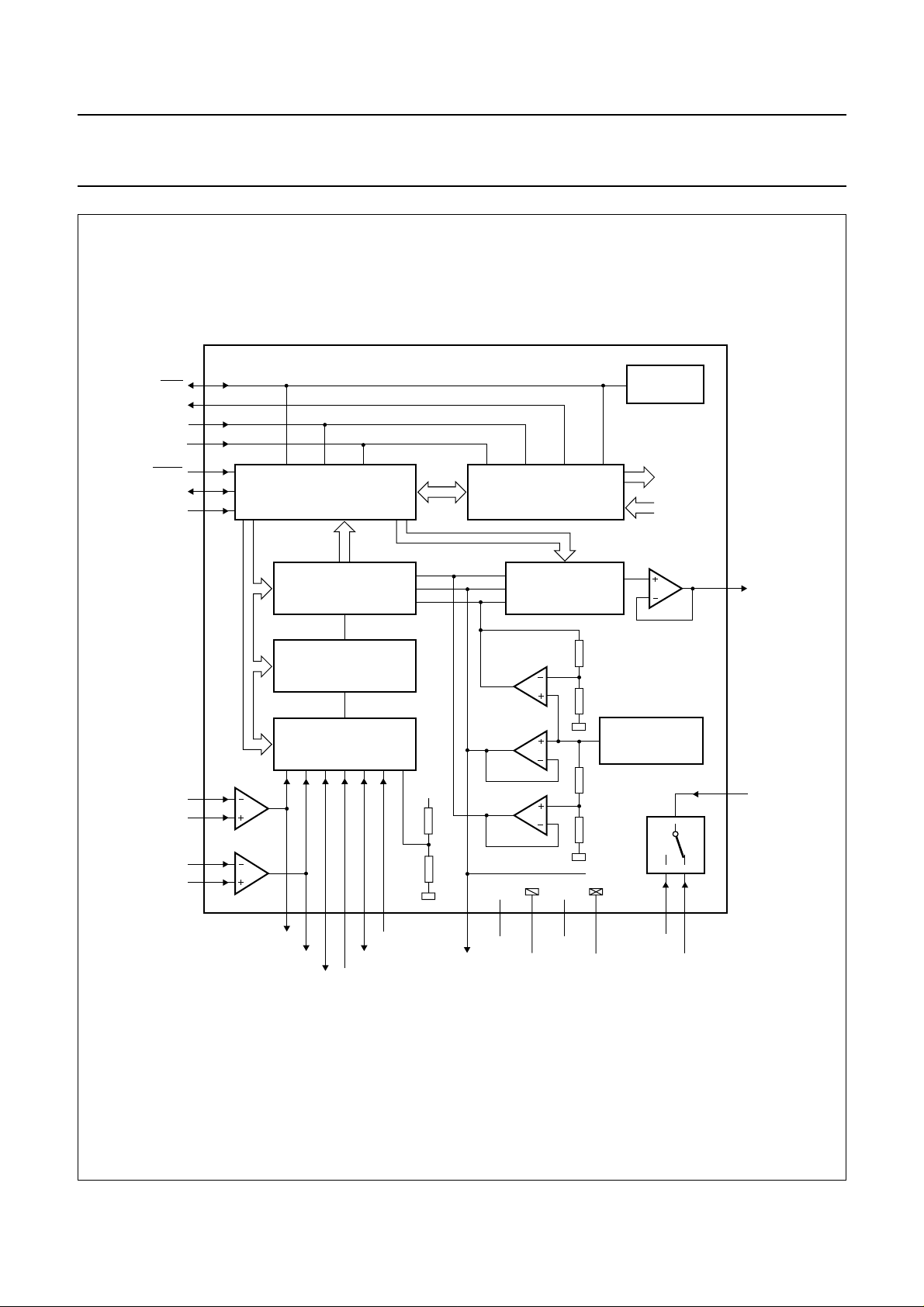
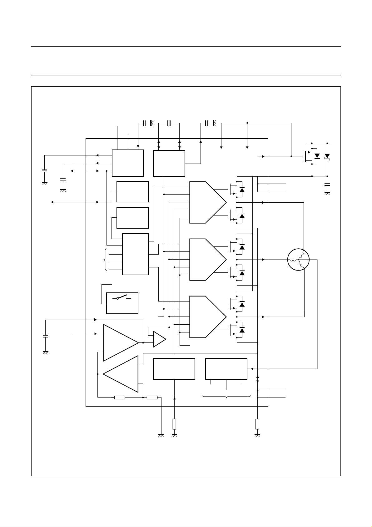
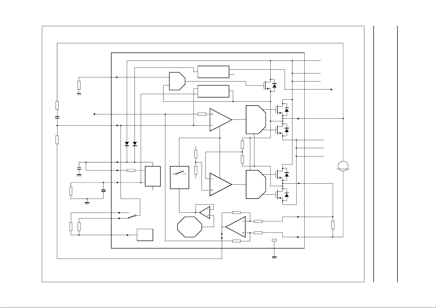
Figures 1, 2, 3 and 4 provide block diagrams of the OM5193H servo and motor control (top level diagram, servo
controller, spindle motor driver and voice coil motor driver).
handbook, full pagewidth
CLAMP1
CLAMP2
CLAMP3
SLEW
SPCCOUT
SPCC
MOTSENSE3
MOTSENSE2
MOTSENSE1/
SPSENSEH
GNDS/SPSENSEL
ZCROSS
CLOCK
SCLOCK
SDEN
SDATA
SCANTEST
V
DDA1
V
DDA2
AGND
INTINN
INTIN
ADC[0]/INTOUT
PESAMPN
PESAMP
ADC[1]/DIFOUT
CT
10
55
56
12
14
13
73
76
2
11
9
25
24
23
21
22
26
44
15
39
37
38
28
35
36
29
CLAMP
A2
A1
MOTA
72
SPINDLE
CONTROL
COMA
COMB
COMC
COMMUTATION
LOGIC
SERIAL
INTERFACE
7-CHANNEL
10-BIT ADC
0 1 2 3 4 5 6
30 31 32 33 34 40 42 41 43 53 52
ADC[2]/SOUT
ADC[3]
MOTB
74
POWER
STAGE
ACROSS
BCROSS
CCROSS
THERMAL
MONITOR
ADC[5]
ADC[4]/TEMP
BRAKEDELAY
MOTC
BRAKEPOWER
3 48 50 49 51
PARK AND BRAKE
THERMAL
SHUTDOWN
OM5193H
10-BIT
VCM DAC
0.5V
DDA1
DACOUT
REF2V5
BANDGAP
VCM
SWITCH
SEEKSELECT
TRACKFWSELECT
PARKVOLT
BRAKEADJH
VCMIN
VCMSENSEL
VCM
CONTROL
VCMSENSEH
1, 4 to 7,
58 to 61, 64 to 67,
70, 75, 78 to 80
18
CHARGE
PUMP
POWER-ON
RESET
POWER
STAGE
CLAMP
20
27
16
17
18
46
47
45
19
57
77
69
71
68
63
54
62
MGM972
8
HEATSINK
V
DDD
DGND
SWITCHGATE
BSTCP1
BSTCP2
CAPY
CHK5
CHK12
CPOR
POR
PWRBIAS1
PWRBIAS2
NIVCM
GNDVCM1
GNDVCM2
GNDVCM3
GNDV
IVCM
Fig.1 Block diagram, top level.
1998 Nov 02 6
Page 7
Philips Semiconductors Product specification
Disk drive spindle and VCM with
servo controller
handbook, full pagewidth
POR
ZCROSS
CLOCK
SCANTEST
SDEN
SDATA
SCLOCK
19
25
24
26
21
22
23
SERIAL INTERFACE COMMUTATION LOGIC
10-BIT ADC
10-BIT VCM DAC
POWER-ON
RESET
COMA
COMB
COMC
ACROSS
BCROSS
CCROSS
OM5193H
34
DACOUT
INTINN
INTIN
PESAMPN
PESAMP
37
A2
38
35
A1
36
ADC[0]/INTOUT
ADC[1]/DIFOUT
ADC[2]/SOUT
RANGE
ADAPTER
INPUT
MULTIPLEXER
30 31 32 33
29
28
ADC[5]
ADC[4]/TEMP
ADC[3]
V
DDA1
V
ref3V5
V
ref2V5
V
ref1V5
V
ref2V5
40 39
V
REF2V5
44
DDA1
AGND DGND
V
20
DDD
OM5193H
2.5 V BANDGAP
VCM switch
for VCM
27
SEEKSELECT
TRACKFWSELECT
VCMIN
414342
MGM973
Fig.2 Block diagram, servo controller.
1998 Nov 02 7
Page 8
Philips Semiconductors Product specification
Disk drive spindle and VCM with
servo controller
handbook, full pagewidth
C
CHK5
C
CHK12
POR
V
DDA1
46CHK5
47CHK12
19
32ADC[4]/TEMP
POWER-ON
C
CPOR
V
DDA2
CPOR BSTCP1 BSTCP2 CAPY PWRBIAS1 PWRBIAS2
44 15 45 16
RESET
THERMAL
MONITOR
THERMAL
SHUTDOWN
C
CAPX
CHARGE
PUMP
C
CAPY
17 18 7757
OM5193H
PREDRIVER
8
SWITCH GATE
10
CLAMP1
55
CLAMP2
56
CLAMP3
72
MOTA
OM5193H
V
DDA2POWER
C
SPCCOUT
SPCCOUT
SPCC
from
commu-
tation
logic
14
13
COMA
COMB
COMC
V
(from VCM)
ref
SPINDLE
SWITCH
CONTROL
AMPLIFIER
SENSE
AMPLIFIER
GNDS/SPSENSEL
DECODER
V
CAPY
SLOPE
CURRENT
CONTROL
1211
SLEW
R
SLEW
PREDRIVER
PREDRIVER
I
(from VCM)
brake
COMPARATOR
ACROSS
to commutation logic
BEMF
BCROSS
MOTSENSE1/
CCROSS
SPSENSEH
74
MOTB
3
MOTC
9
CT
MOTSENSE2
76
MOTSENSE3
73
2
R
SPSENSE
MGM974
Fig.3 Block diagram, spindle motor driver.
1998 Nov 02 8
Page 9
This text is here in white to force landscape pages to be rotated correctly when browsing through the pdf in the Acrobat reader.This text is here in
a
_white to force landscape pages to be rotated correctly when browsing through the pdf in the Acrobat reader.This text is here inThis text is here in
white to force landscape pages to be rotated correctly when browsing through the pdf in the Acrobat reader. white to force landscape pages to be ...
1998 Nov 02 9
VCMIN
51
PARK
40
43
48
49
BRAKE
50
AFTER
PARK
I
brake
(to spindle)
SWITCH
V
(to spindle)
ref
R
VCMCOMPRC
C
VCMCOMPRC
R
FEEDBACK
C
BRAKEP
R
R
PARKVOLT
BRAKEPOWER
BRAKEDELAY
BRAKED
C
BRAKED
PARKVOLT
REF2V5
BRAKEADJH
ndbook, full pagewidth
POWER-DOWN
PRECHARGE
12 V
GND
ERROR
ERROR
ERROR
master
slave
V
CAPY
PRE
DRIVER
PRE
DRIVER
OM5193H
10
CLAMP1
55
CLAMP2
56
CLAMP3
8
SWITCHGATE
62
IVCM
71
GNDVCM1
68
GNDVCM2
63
GNDVCM3
69
NIVCM
Philips Semiconductors Product specification
Disk drive spindle and VCM with
servo controller
M
TRACKFWSELECT
R
VCMTRACKFW
SEEKSELECT
R
VCMSEEK
DACOUT
42
41
34
VCM switch
BANDGAP
VCM
DAC
Fig.4 Block diagram, voice coil motor driver.
SENSE
30
ADC[2]/SOUT GNDV
54
53
VCMSENSEL
R
52
VCMSENSEH
VCMSENSE
MGM975
OM5193H
Page 10

Philips Semiconductors Product specification
Disk drive spindle and VCM with
OM5193H
servo controller
7 PINNING
SYMBOL PIN I/O DESCRIPTION
HEATSINK 1 − dissipation pin; internally connected to the leadframe
MOTSENSE1/SPSENSEH 2 analog I/O sense line of the spindle/spindle sense amplifier input
MOTC 3 analog output spindle motor power output
HEATSINK 4 − dissipation pin; internally connected to the leadframe
HEATSINK 5 − dissipation pin; internally connected to the leadframe
HEATSINK 6 − dissipation pin; internally connected to the leadframe
HEATSINK 7 − dissipation pin; internally connected to the leadframe
SWITCHGATE 8 analog output isolation FET driver
CT 9 analog input centre tap of the spindle
CLAMP1 10 supply power stage supply voltage
GNDS/SPSENSEL 11 ground spindle ground connection/spindle sense amplifier ground
SLEW 12 analog input spindle motor slope control
SPCC 13 analog input spindle current control
SPCCOUT 14 analog input compensation point of the spindle current control loop
V
DDA2
BSTCP1 16 analog I/O booster capacitor 1
BSTCP2 17 analog I/O booster capacitor 2
CAPY 18 analog output DC-to-DC converter output (19 V)
POR 19 digital I/O power-on reset signal; active LOW
V
DDD
SDEN 21 digital input serial interface data enable; active LOW
SDATA 22 digital I/O serial interface data line
SCLOCK 23 digital input serial interface clock line
CLOCK 24 digital input clock input
ZCROSS 25 digital output zero crossing detection signal
SCANTEST 26 digital input scantest mode control; at LOW-level in normal conditions
DGND 27 ground servo digital ground
ADC[0]/INTOUT 28 analog I/O ADC channel 0 input/output of the A2 amplifier
ADC[1]/DIFOUT 29 analog I/O ADC channel 1 input/output of the A1 amplifier
ADC[2]/SOUT 30 analog I/O ADC channel 2 input/VCM sense amplifier output
ADC[3] 31 analog input ADC channel 3 input
ADC[4]/TEMP 32 analog I/O ADC channel 4 input/temperature monitor, thermal shutdown
ADC[5] 33 analog input ADC channel 5 input
DACOUT 34 analog output 10-bit VCM DAC output
PESAMPN 35 analog input inverting input of the A1 amplifier.
PESAMP 36 analog input non-inverting input of the A1 amplifier
INTINN 37 analog input inverting input of the A2 amplifier
INTIN 38 analog input non-inverting input of the A2 amplifier
AGND 39 ground servo analog ground
REF2V5 40 analog output 2.5 V bandgap reference voltage
15 supply 12 V analog supply voltage
20 supply 5 V digital supply voltage
1998 Nov 02 10
Page 11

Philips Semiconductors Product specification
Disk drive spindle and VCM with
OM5193H
servo controller
SYMBOL PIN I/O DESCRIPTION
SEEKSELECT 41 analog input input for the seek mode
TRACKFWSELECT 42 analog input input for the track-following mode
VCMIN 43 analog input VCM control input
V
DDA1
CPOR 45 analog input set the
CHK5 46 analog output set the V
CHK12 47 analog output set the V
BRAKEPOWER 48 analog input brake power capacitor
BRAKEADJH 49 analog input adjust current consumption during park mode
BRAKEDELAY 50 analog input set the brake-after-park delay time
PARKVOLT 51 analog input set the park voltage
VCMSENSEH 52 analog input positive input of the VCM sense amplifier
VCMSENSEL 53 analog input negative input of the VCM sense amplifier
GNDV 54 ground VCM ground connection
CLAMP2 55 supply power stage supply voltage
CLAMP3 56 supply power stage supply voltage
PWRBIAS1 57 analog input power stages isolation bias; externally connected to the clamp
HEATSINK 58 − dissipation pin; internally connected to the leadframe
HEATSINK 59 − dissipation pin; internally connected to the leadframe
HEATSINK 60 − dissipation pin; internally connected to the leadframe
HEATSINK 61 − dissipation pin; internally connected to the leadframe
IVCM 62 analog output inverted output of the VCM (master stage)
GNDVCM3 63 ground VCM power stage ground
HEATSINK 64 − dissipation pin; internally connected to the leadframe
HEATSINK 65 − dissipation pin; internally connected to the leadframe
HEATSINK 66 − dissipation pin; internally connected to the leadframe
HEATSINK 67 − dissipation pin; internally connected to the leadframe
GNDVCM2 68 ground VCM power stage ground
NIVCM 69 analog output non-inverted VCM output (slave stage)
HEATSINK 70 − dissipation pin; internally connected to the leadframe
GNDVCM1 71 ground VCM power stage ground
MOTA 72 analog output spindle motor power output
MOTSENSE3 73 analog output sense line of the spindle
MOTB 74 analog output spindle motor power output
HEATSINK 75 − dissipation pin; internally connected to the leadframe
MOTSENSE2 76 analog output sense line of the spindle
PWRBIAS2 77 analog input power stages isolation bias; externally connected to the clamp
HEATSINK 78 − dissipation pin; internally connected to the leadframe
HEATSINK 79 − dissipation pin; internally connected to the leadframe
HEATSINK 80 − dissipation pin; internally connected to the leadframe
44 supply 5 V analog supply voltage
POR delay time
POR threshold
DDA1
POR threshold
DDA2
1998 Nov 02 11
Page 12
Philips Semiconductors Product specification
Disk drive spindle and VCM with
servo controller
handbook, full pagewidth
PWRBIAS2
HEATSINK
78
77
HEATSINK
MOTSENSE1/
SPSENSEH
MOTC
HEATSINK
HEATSINK
HEATSINK
HEATSINK
SWITCHGATE
CT
CLAMP1
GNDS/SPSENSEL
SLEW
SPCC
SPCCOUT
V
DDA2
BSTCP1
BSTCP2
CAPY
POR
V
DDD
SDEN
SDATA
SCLOCK
CLOCK
10
11
12
13
14
15
16
17
18
19
20
21
22
23
24
1
2
3
4
5
6
7
8
9
HEATSINK
HEATSINK
80
79
MOTSENSE2
HEATSINK
MOTB
76
75
74
MOTSENSE3
73
OM5193H
MOTA
72
GNDVCM1
HEATSINK
71
70
NIVCM
69
GNDVCM2
HEATSINK
68
67
HEATSINK
HEATSINK
66
65
OM5193H
HEATSINK
64
GNDVCM3
63
IVCM
62
HEATSINK
61
HEATSINK
60
HEATSINK
59
HEATSINK
58
PWRBIAS1
57
CLAMP3
56
CLAMP2
55
GNDV
54
VCMSENSEL
53
VCMSENSEH
52
PARKVOLT
51
BRAKEDELAY
50
BRAKEADJH
49
BRAKEPOWER
48
CHK12
47
CHK5
46
CPOR
45
V
44
DDA1
VCMIN
43
TRACKFWSELECT
42
SEEKSELECT
41
25
26
27
28
29
30
31
32
ZCROSS
SCANTEST
DGND
ADC[0]/INTOUT
ADC[1]/DIFOUT
ADC[3]
ADC[2]/SOUT
ADC[4]/TEMP
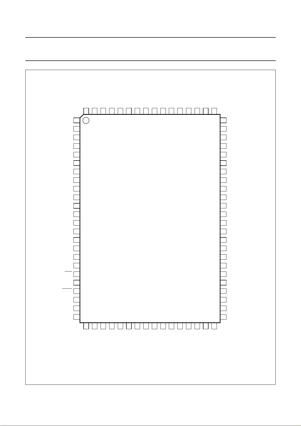
Fig.5 Pin configuration.
1998 Nov 02 12
33
ADC[5]
34
35
DACOUT
PESAMPN
36
37
INTINN
PESAMP
38
INTIN
39
AGND
40
MGM976
REF2V5
Page 13
Philips Semiconductors Product specification
Disk drive spindle and VCM with
servo controller
8 FUNCTIONAL DESCRIPTION
8.1 Serial interface
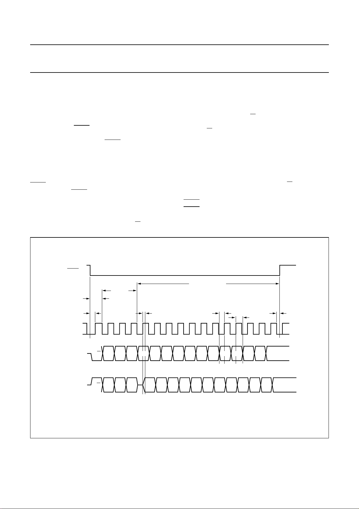
The serial interface is a 3-wire bidirectional port for writing
and reading data to and from the internal registers of the
OM5193H. Each read or write will be composed of 16 bits.
For data transfer
presented at the SDATA pin, and a serial clock is applied
to the SCLOCK pin. After the SDEN pin goes LOW, the
first 16 pulses applied to the SCLOCK pin shift the data
presented at the SDATA pin into an internal shift register
on the rising edge of each clock pulse. An internal counter
prevents more than 16 bits from being shifted into the
register. The data in the shift register is latched when
SDEN goes HIGH. If less than 16 clock pulses are
provided before SDEN goes HIGH, the data transfer is
aborted.
All transfers are shifted into the serial port with the MSB
first. The first 4 bits of the transfer contain address and
instruction information. The MSB is the R/W bit which
SDEN is brought LOW, serial data is
OM5193H
determines if the transfer is a read (logic 1) or a
write (logic 0).
The remaining 3 bits determine the internal register to be
accessed. The other 12 bits contain the programming
data. In the read mode (R/
the register contents of the selected address. In the write
mode (R/W = 0), the OM5193H loads the selected register
with the data presented on the SDATA pin. During sleep
mode, the serial port remains active and register
programmed data is retained.
SCLOCK is driven by the microcontroller. When the
microcontroller drives the SDATA line, the data is valid on
the rising edge of SCLOCK. When the OM5193H is driving
the SDATA line (in read mode after the R/W bit and 3 bits)
the data is valid on the falling edge of SCLOCK.
SDEN marks the end of the serial transfer. When the
SDEN pin goes HIGH, the shift register data is latched into
the addressed register of the OM5193H.
W = 1), the OM5193H outputs
handbook, full pagewidth
SDEN
SCLOCK
SDATA
Write to the OM5193H
SDATA
Write to, then read from the OM5193H
send/receive data
address
direction
325476981110 1312 14 1615 1
t
st
R/W
R/W
A1A2 D11A0 D9D10 D7D8 D5D6 D3D4 D2 D0D1
write registers read back data
A1A2 D11A0 D9D10 D7D8 D5D6 D3D4 D2 D0D1
t
ren
t
su
t
hd
t
ex
MGM977
Fig.6 Serial port timing information.
1998 Nov 02 13
Page 14
Philips Semiconductors Product specification
Disk drive spindle and VCM with
OM5193H
servo controller
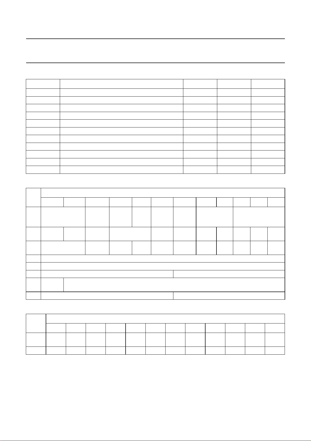
Table 1 Timing information for the serial interface
SYMBOL PARAMETER MIN. MAX. UNIT
f
clk
t
st
t
su
t
hd
t
rd
t
ren
t
rhd
t
rsu
t
exW
t
exR
T
bpa
Table 2 Writeable registers of the serial interface
REG
0 not used
1 reverse
break
2 not used
3 not used
4 not used
5 Watchdog Blank 1
6 high
Clock_N
7 Start-up Blank 2
clock frequency − 30 MHz
chip select to first active clock edge
1
⁄2T
clk
− ns
data to clock set-up time 12 − ns
clock to data hold time 12 − ns
time data line is driven after 5th negative clock − 5ns
time from positive clock for data line to be driven 0 − ns
receive data hold time 0 − ns
receive data set-up time 12 − ns
last active clock to chip select; inactive on write 0 − ns
last active clock to chip select; inactive on read 10 − ns
time between successive serial port accesses 5 − clock cycles
BITS
11 10 9 8 7 6 5 4 3210
auto
Conv.
select
range
Select
test
Mode_N
not used ADC MUX address
not used sleep_N spindiv manual
DAC
(7)
DAC
(6)
DAC
(5)
DAC
(4)
run/
comC comB comA
stop
DAC
(3)
DAC
(2)
DAC
(1)
not
used
opamp
Select_N
seek/
trackfw
DAC
(9)
increm.
Channel
DAC
(8)
Comdelim
DAC
(0)
Table 3 Readable registers of the serial interface
BITS
REG
11109876543210
0 ADC
status
ADC
(9)
ADC
(8)
ADC
(7)
ADC
(6)
ADC
(5)
ADC
(4)
ADC
(3)
ADC
(2)
ADC
(1)
1 Ccross Bcross Across
1998 Nov 02 14
ADC
(0)
Page 15
Philips Semiconductors Product specification
Disk drive spindle and VCM with
OM5193H
servo controller
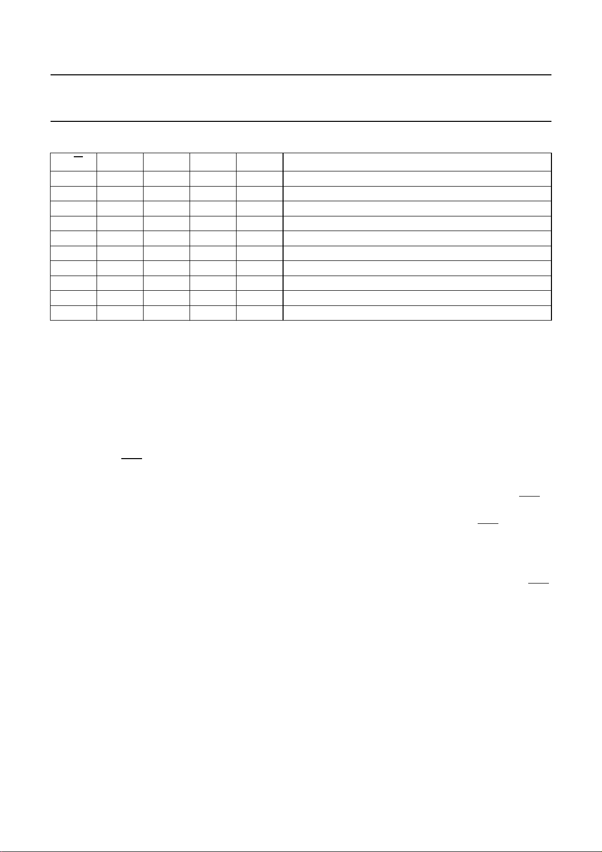
Table 4 Address of registers
R/W A2 A1 A0 REG. DESCRIPTION
00000ADC channel and programmable options
10000ADC status and value
00011commutation, sleep, and VCM switch controls
10011commutation state in manual mode
0010210-bit DAC
00113not used
01004not used
01015Blank 1 and Watchdog delays
01106commutation delay limit (11 bits), internal clock divider factor
01117Start-up and Blank 2 delays
8.2 Commutation and sleep mode
Spindle control and sleep mode are controlled by writing or
reading on register#1.
• Register#1 (0, 1 and 2) control the spindle
commutations in manual mode when run/stop, manual
and sleep bits are correctly set. The commutation
sequence is described in Section “Spindle driver” (see
also Table 16 and Fig.12).
• Register#1 (3) is the run/stop bit. After the power is
turned on and POR is HIGH, the motor will not start
spinning until register#1 (3) has been set to logic 1.
The motor stops spinning when this bit is set to logic 0.
• Register#1 (4) is the manual commutation mode bit.
When this bit is set to logic 1 and register#1 (3) set to
logic 1, the commutation logic in the OM5193H will be
disabled so that the spindle will not automatically go to
the next commutation.
When register#1 (3 and 4) are set to logic 1, the
microcontroller is expected to generate the different
commutation states for the motor. The OM5193H will
still provide the coil status which will be available by
reading register#1. The different waveforms are shown
in Section “Spindle driver” (see also Fig.12). Note that
depending on the coil status acquisition moment,
transient states (due to the flyback pulses) can be read.
When register#1 (4) is set to logic 0, the manual mode
is disabled and the OM5193H will automatically
commutate the motor each time a zero crossing is
detected. The time between the zero crossing and the
next commutation is half the time between the two
preceding zero crossings. This is explained in the
detailed description in Section “Commutation control”.
• Register#1 (5) is the spindiv bit. This bit together with
register#6 (11) enables the selection of a divider factor
for both converter clock and spindle clock. Clock
configurations are described in Section “Commutation
control” (see also Table 6).
• Register#1 (6) is the sleep mode bit. When it is set to
logic 0, the OM5193H will enter the low power mode.
Then the commutation control generates (101) output
codes on commutation signals to set spindle and VCM
head into sleep mode. This causes the OM5193H to go
into the brake-after-park mode. The only operating
circuits are the power monitor, the voltage reference
generator, the VCM precharge circuit and the serial
interface. The OM5193H is in sleep mode when
LOW.
When the power is first turned on, the POR signal goes
HIGH after the POR delay. The OM5193H is then
automatically set in sleep mode and thus in low power
consumption mode. The VCM DAC output is in
high-impedance mode, the spindle is in the brake mode
and the VCM is in the precharge mode. Only after POR
is HIGH and register#1 (6) is set to logic 1, OM5193H is
ready to be functional. When register#1 (6) goes HIGH,
the VCM DAC outputs the 2.5 V reference voltage.
• Register#1 (11) is dedicated to brake the spindle motor
without going in ‘brake-after-park’ mode.
The commutation sequence is shifted in order to
efficiently brake the motor. This brake, called reverse
brake, is activated when register#1 (11) bit is set to
logic 1. Note that there is no action on the VCM input
signal when the reverse brake is used. When this bit is
set to logic 0, the spindle motor starts again with normal
spindle commutations.
POR is
1998 Nov 02 15
Page 16

Philips Semiconductors Product specification
Disk drive spindle and VCM with
OM5193H
servo controller
Reading register#1 will read the state of the 3 coils coming
from the spindle control block (ACROSS, BCROSS and
CCROSS). The 3 input lines will be in bits 0, 1, and 2.
The different waveforms are shown in Section “Spindle
Table 5 Writing register#1
BIT
0 0 comA drives COMA when in manual commutation
1 0 comB drives COMB when in manual commutation
2 0 comC drives COMC when in manual commutation
3 0 run/stop 0 = motor to brake-after-park mode
4 0 manual 0 = automatic commutation mode with run/stop = 1
5 0 spindiv 0 = the internal spindle clock frequency is controlled by register#6 (11)
6 0 sleep_N 0 = sleep mode: low power mode, serial interface active, power stages in
70− not used
80− not used
9 1 seek/trackfw 0 = VCMIN connected to SEEKSELECT
10 1 − not used
11 0 reverse break 1 = active brake control
DEFAULT
VALUE
NAME DESCRIPTION
1 = motor spinning; VCM active
1 = manual commutation mode with run/stop = 1
(bit highClock_N)
1 = an additional divider by 4 is added on the internal spindle clock
brake-after-park mode
1 = fully functional mode: sleep_N has higher priority than run/stop if both are
active
1 = VCMIN connected to TRACKFWSELECT
0 = normal commutations as defined by bits above
driver” (see also Fig.12). Note that depending on the coil
status acquisition moment, transient states (due to the
flyback pulses) can be read.
8.3 Commutation control
The commutation logic block generates the six different
states to rotate the spindle motor. The spindle driver block
provides the BEMF zero crossing information.
The commutation block interprets the zero crossing
information and determines the commutation delay time
and the next coil state. The commutation block must take
into account the following situations:
• Start-up
• No start
• Reverse rotating
• Run
• Manual commutation.
1998 Nov 02 16
The commutation logic keeps the motor spinning by
commutating the motor after each detected zero crossing.
It measures the time between two successive BEMF zero
crossings and then determines the next commutation.
The delay (commutation delay) between a zero crossing
and the next commutation is half the time between the two
preceding zero crossings. The commutation delay
(Comdelim) can be limited to guarantee a faster lock after
the motor has gone out of lock. A maximum commutation
delay can be set via the serial port. The time is a function
of both the external clock frequency, the individual register
prescalers and the time programmed into the registers.
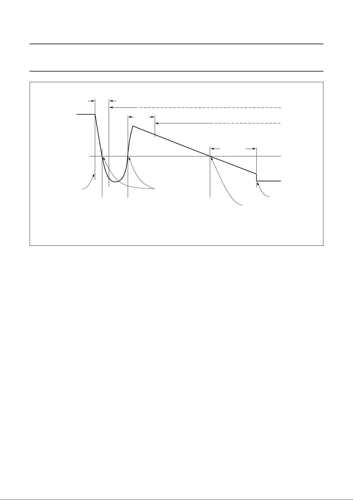
Figure 7 shows a typical motor commutation timing
diagram.
Page 17
Philips Semiconductors Product specification
Disk drive spindle and VCM with
servo controller
handbook, full pagewidth
Blank 1
centre tap
commutation
Zc
1
flyback pulse
Watchdog
Zc
2
Blank 2
Start-up
false zero crossings
Zc
3
Commutation
delay
OM5193H
commutation
true zero crossing
MGM978
Fig.7 A typical motor commutation diagram.
• Blank 1
After a commutation occurs, the leading edge of the
flyback pulse has a zero crossing (Zc1). Blank 1 timer is
used to ignore this zero crossing by masking it while the
timer initialized at Blank 1 value is counting. The state
associated to Blank 1 down-counter will end when the
counter reaches the zero value.
• Blank 2
The Blank 2 timer starts counting as soon as the second
zero crossing occurs (Zc2). After the second flyback
pulse zero crossing, all extra zero crossings are ignored
during the Blank 2 time. This allows the ringing of the
coil voltage without causing a commutation advance.
The state associated to Blank 2 down-counter will end
when the counter reaches the zero value.
• Watchdog
The Watchdog timer makes sure the motor is running in
forward direction. If the motor is rotating in reverse
direction, the BEMF voltage is inverted and the second
crossing of the flyback pulse (Zc2) will not occur until the
true BEMF zero crossing is detected. Therefore, if the
Watchdog timer expires before a zero crossing occurs,
the motor is assumed to be rotating backwards.
The commutation is advanced by one step to correct
this condition. The Watchdog time must be set to a value
that is greater than the flyback pulse duration, measured
when the spindle motor stands still.
The state associated to the Watchdog timer will start
when the one associated to Blank 1 timer is finished and
will end when Zc2 occurs or when the Watchdog counter
expires.
• Start-up
If the motor is not spinning, the BEMF zero crossings will
not occur. The Start-up timer detects this if it expires
before the true zero crossing (Zc3) has occurred. It will
advance the commutation by one step if this happens.
The state associated to Start-up timer will start when the
one associated to Blank 2 timer is finished and will end
when Zc3 occurs or when Start-up expires.
• Comdelim
The timer associated to Comdelim value allows to
control the maximum commutation delay (between zero
crossing and next commutation). When the true zero
crossing is detected (Zc3), the timer will count until it
expires and then will commutate the motor to the next
step. This commutation delay time is equal to half the
measured value between 2 zero crossings.
The Comdelim value should be set to the maximum
allowable delay value. If ∆Zc
is lower than the
meas
programmed Comdelim value, the next timer value will
be ∆Zc
divided by 2. If ∆Zc
meas
is higher than the
meas
programmed Comdelim value, the next timer value will
be the programmed Comdelim value divided by 2.
1998 Nov 02 17
Page 18

Philips Semiconductors Product specification
Disk drive spindle and VCM with
OM5193H
servo controller
The clock used in the commutation logic block is obtained
by dividing the master clock of the chip (f
CLOCK
) by a clock
divider (Prescaler). This internal clock will be named
internalSpindleClock. Internal spindle clock configurations
are described in Table 6.
Table 6 Spindle clock configurations
spindiv
REGISTER#1 (5)
highClock_N
REGISTER#6 (11)
00
01
10
11
8.3.1 B
LANKS,WATCHDOG AND START-UP DELAYS
An internal down-counter called TIMER 1 is used to generate Blank 1, Blank 2, Watchdog and Start-up delays. It loads
one of these programmed values and counts down till it reaches zero.
All the delays described above (Blank 1, Watchdog,
Blank 2, Start-up and Comdelim) are generated by one
down-counter (called TIMER 1), see Fig.8 and one
up-counter (called TIMER 2), see Fig.9. Each of them
uses internalSpindleClock signal.
internalSpindleClock
1
⁄
16fCLOCK
1
⁄
32fCLOCK
1
⁄
64fCLOCK
1
⁄
128fCLOCK
handbook, full pagewidth
19
18 15 14 13 12 11 1017 16 9 8 5 4 3 2 1 07 6
Start-up
Fig.8 Down-counter TIMER 1.
The actual delay time will be:
Delay value step×=
Value is the decimal representation of the binary code
programmed in one of the 6 bit registers.
LSB
Step
=
--------------------------------------------------------------internalSpindleClock
2
Blank 1
Blank 2
Watchdog
MSB 1+()
2
maxValue
(1)
------------------------------------------------------
=
internalSpindleClock
We have to subtract (2
(2)
because all the bits from 0 to (LSB − 1) are set internally to
=
----------------------------------------------------------------------------
MSB 1+()
2
internalSpindleClock
LSB
2
–
LSB
1–
–
− 1) to obtain maxValue
MGL481
LSB
1–
2
zero by design.
(3)
1998 Nov 02 18
Page 19
Philips Semiconductors Product specification
Disk drive spindle and VCM with
OM5193H
servo controller
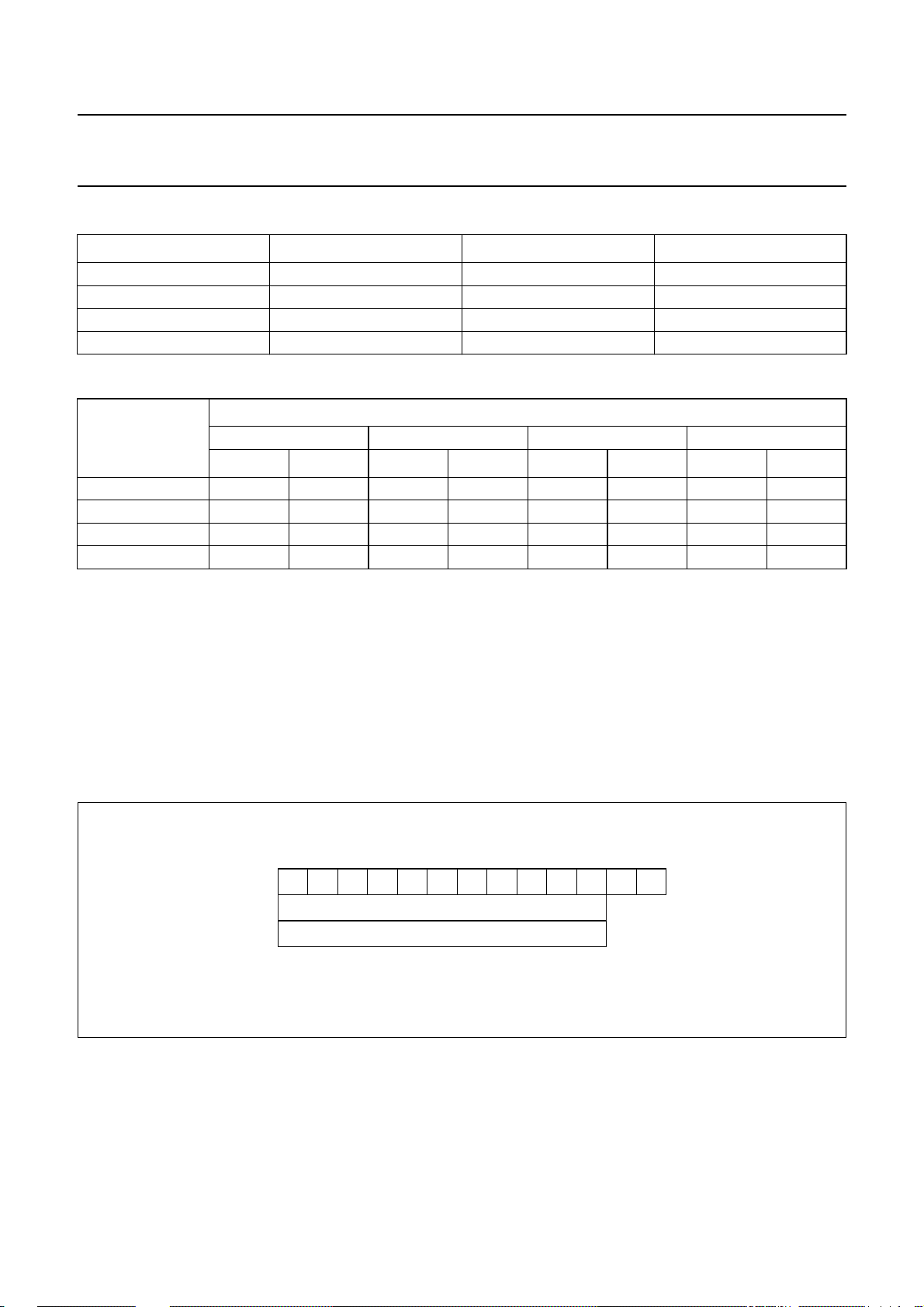
Table 7 Delays used for TIMER 1
DELAY LSB MSB BITS
Blank 1 2 7 6
Blank 2 5 10 6
Watchdog 7 12 6
Start-up 14 19 6
Table 8 Numerical application with f
1
DELAYS
⁄16f
CLOCK
STEP MAX. STEP MAX. STEP MAX. STEP MAX.
Blank 1; note 1 2.13 µs 134 µs 4.27 µs 269 µs 8.53 µs 538 ms 17.1 µs 1.08 ms
Blank 2; note 2 17.1 µs 1.08 ms 34.1 µs 2.15 ms 68.3 µs 4.30 ms 137 µs 8.60 ms
Watchdog; note 3 68.3 µs 4.30 ms 137 µs 8.60 ms 273 µs 17.2 ms 546 µs 34.4 ms
Start-up; note 4 8.74 ms 550 ms 17.5 ms 1.101 s 35 ms 2.202 s 70 ms 4.404 s
Notes
1. The first zero crossing of the flyback should occur within this time.
2. The real zero crossing should not come within this time after the second zero crossing of the flyback pulse.
3. The time should be larger than the duration of the flyback pulse measured when the motor stands still.
4. The actual zero crossing should occur within this time after the Blank 2 time has expired.
CLOCK
= 30 MHz
internalSpindleClock
1
⁄32f
CLOCK
1
⁄64f
CLOCK
1
⁄
128fCLOCK
8.3.2 C
OMDELIM DELAY
An internal up-counter called TIMER 2 is used to measure the time between two zero crossings and also to set the
maximum commutation delay through Comdelim delay.
handbook, full pagewidth
12 11 10 9 8 5 4 3 2 1 07 6
Comdelim
MGL482
Fig.9 Up-counter TIMER 2.
1998 Nov 02 19
Page 20
Philips Semiconductors Product specification
Disk drive spindle and VCM with
OM5193H
servo controller
Comdelim is the maximum value that can be reached by TIMER 2. So, this is the maximum time between 2 zero
crossings (∆Zc). The maximum commutation delay (Comdelim delay) is then half this value.
The actual delay will be:
∆Zc value step× Offset+=
ComdelimDelay
Value is the decimal representation of the binary code programmed in the 11-bit register.
Step
=
--------------------------------------------------------------internalSpindleClock
Offset
=
--------------------------------------------------------------internalSpindleClock
(we have to add this offset because bits 0 and 1 are set internally to logic 1 by design).
maximum∆Zc
maximumComdelimDelay
∆Zc
=
---------- 2
LSB
2
3
MSB 1+()
=
2
--------------------------------------------------------------internalSpindleClock
=
--------------------------------------------------------------internalSpindleClock
1–
MSB()
2
1
–
-- 2
(4)
(5)
(6)
(7)
(8)
(9)
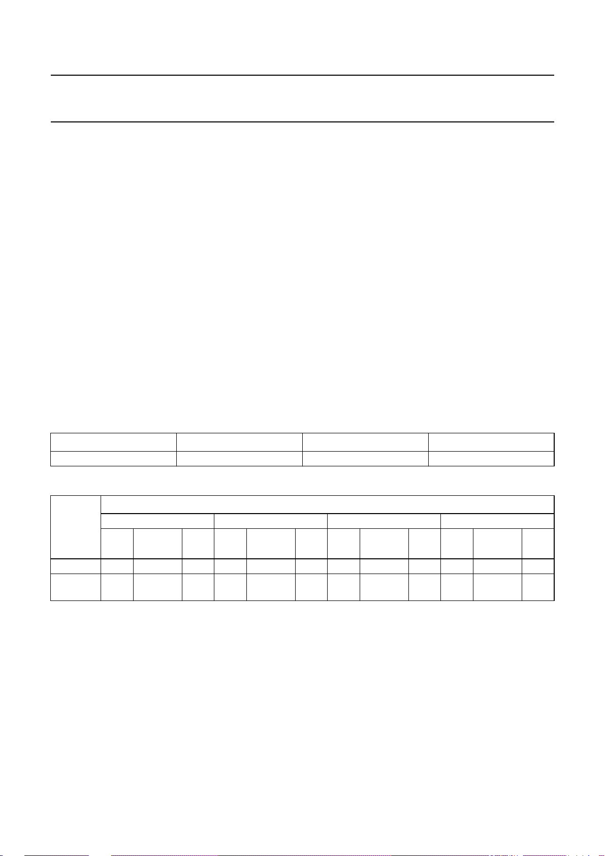
Table 9 Delay used for TIMER 2
DELAY LSB MSB BITS
Comdelim 2 12 11
Table 10 Numerical application with f
CLOCK
= 30 MHz
CLOCKOUT/PRESCALER
DELAYS
STEP
(µs)
1
⁄16f
CLOCK
OFFSET
(µs)
MAX.
(ms)
STEP
(µs)
1
⁄32f
CLOCK
OFFSET
(µs)
MAX.
(ms)
STEP
(µs)
1
⁄64f
CLOCK
OFFSET
(µs)
MAX.
(ms)
STEP
(µs)
1
⁄
128fCLOCK
OFFSET
(µs)
MAX.
(ms)
∆Zc 2.13 1.6 4.37 4.27 3.2 8.74 8.53 6.4 17.48 17.1 12.8 35
Comdelim
1.07 0.8 2.18 2.13 1.6 4.37 4.27 3.2 8.74 8.53 6.4 17.48
delay
The commutation delay counter, which starts counting at a zero crossing, has two operating modes:
• In the adaptive mode, the next zero crossing is detected before the commutation delay counter has reached its
programmed value. In this mode, the next commutation will occur at the measured t
divided by 2 after the last
Zcross
zero crossing.
• In the forced mode, the next zero crossing is detected after the commutation delay counter reaches its programmed
value. In this mode, the counter is stopped and the commutation logic block waits until the next zero crossing occurs.
After it occurs, the next commutation will be forced at the programmed commutation delay divided by 2.
1998 Nov 02 20
Page 21

Philips Semiconductors Product specification
Disk drive spindle and VCM with
servo controller
8.4 10-bit ADC with 7 analog inputs
The ADC is a signed 10-bit converter which uses the
successive approximation conversion technique.
The overall accuracy is 2% absolute error not including
contribution of the reference voltage and guaranteed
monotonicity.
8.4.1 I
7 analog input channels can be sampled and converted:
• Channel 0: conversion of the op-amp A2 output
• Channel 1: conversion of the op-amp A1 output
• Channel 2: conversion of the VCM sense amplifier
output
• Channel 3: conversion of an analog external signal
• Channel 4: conversion of the temperature
monitor + temperature shutdown signal
• Channel 5: conversion of an analog external signal
• Channel 6: conversion of an internal signal, controlling
analog supply voltage over two ranges.
NPUT CHANNELS
OM5193H
Channels 0 and 1 can be used as external inputs by
deactivating the 2 stand-alone op-amps A1 and A2
(op-amps are put in sleep mode), that means by putting
register#0 (9) at logic 1.
The ADC does not include input filtering. If this is required
in the application then it must be implemented externally.
8.4.2 I
Two analog input ranges are possible: either between
1.5 and 3.5 V or between 0 and 5 V. The input range is
selected with register#0 (6):
• Register#0 (6) = 0: means input analog value between
1.5 and 3.5 V
• Register#0 (6) = 1: means input analog value between
0and5V.
NPUT RANGES
Table 11 Input analog voltage and corresponding output code
BIT MIN. OUTPUT = 200H MIDDLE OUTPUT = 000H MAX. OUTPUT = 1FFH
register#0 (6) = 0 minimum input value = 1.5 V middle input value = 2.5 V maximum input value = 3.5 V
register#0 (6) = 1 minimum input value=0V middle input value = 2.5 V maximum input value = 5 V
8.4.3 CONVERSION MODES
Three different conversion modes are possible depending
on the states of register#0 (7) and register#0 (8):
• Auto conversion and input channel auto incrementation
mode.
This mode is obtained with register#0 (7) = 1 and
register#0 (8) = 1. The conversion sequence works as
follows: the first A/D conversion is started by writing to
serial port register#0. The address of the channel is
decoded from the three LSBs in register#0 [2 to 0].
Then the OM5193H selects the addressed analog
channel, samples and holds the analog input and starts
the analog to digital conversion. The conversion result is
obtained by reading the serial port register#0.
Register#0 (10) provides the status of the conversion: it
is set to 0 as long as the conversion is running and
indicates that the low 10 bits of register#0 are invalid.
Register#0 (10) going HIGH means the conversion is
complete and guarantees the validity of the data in
register#0 [9 to 0].
• Auto conversion on the same channel.
This input channel automatic incrementation option can
be deactivated by setting register#0 (8) to logic 0 with
register#0 (7) at logic 1. So the behaviour of the ADC is
the same as explained above, except that all the
conversions are made on the channel specified by the
last write access on register#0.
• Single conversion mode.
The automatic conversion mode can also be
deactivated by setting register#0 (7) to logic 0. In this
mode, a write access on register#0 will start a
conversion on the specified channel and a read access
will not launch any other conversion.
1998 Nov 02 21
Page 22

Philips Semiconductors Product specification
Disk drive spindle and VCM with
OM5193H
servo controller
8.4.4 PROGRAMMING REGISTER#0
Table 12 Writing register#0
BIT DEFAULT VALUES NAME DESCRIPTION
0 ADC MUX address; note 1 ADC MUX address 0
1 ADC MUX address 1
2 ADC MUX address 2
3 not used
4 not used should be at logic 0 under normal operating
conditions
5 0 testMode_N dedicated for test purposes of the DAC in ADC or
DAC mode; should be at logic 0 under normal
operating conditions
6 0 rangeSelect selects the analog input range of the ADC:
0 = range 1.5 to 3.5 V
1 = range 0 to 5 V
7 0 autoConvSelect selects the automatic conversion option; see details
in Table 13
8 0 incrementChannel selects the automatic channel increment option; see
details in Table 13
9 0 opampSelect_N selects the stand-alone op-amps:
0 = op-amps activated
1 = op-amps deactivated
10 not used
11 not used
Note
1. Possible addresses:
a) ADC MUX address = 000: channel 0 selected;
b) ADC MUX address = 001: channel 1 selected;
c) ADC MUX address = 010: channel 2 selected;
d) ADC MUX address = 011: channel 3 selected;
e) ADC MUX address = 100: channel 4 selected;
f) ADC MUX address = 101: channel 5 selected;
g) ADC MUX address = 110: channel 6 selected;
h) ADC MUX address = 111 is an illegal address. No analog input will be selected if a conversion is asked in this
channel and the ADC will convert a random analog value.
For a correct initialization of the converter just after power up, when
the register#0 has to be programmed as follows: write 020H and then write 000H. A read of register#0 between the
2 write accesses is not necessary.
1998 Nov 02 22
POR is HIGH (before using the ADC or the DAC),
Page 23
Philips Semiconductors Product specification
Disk drive spindle and VCM with
OM5193H
servo controller
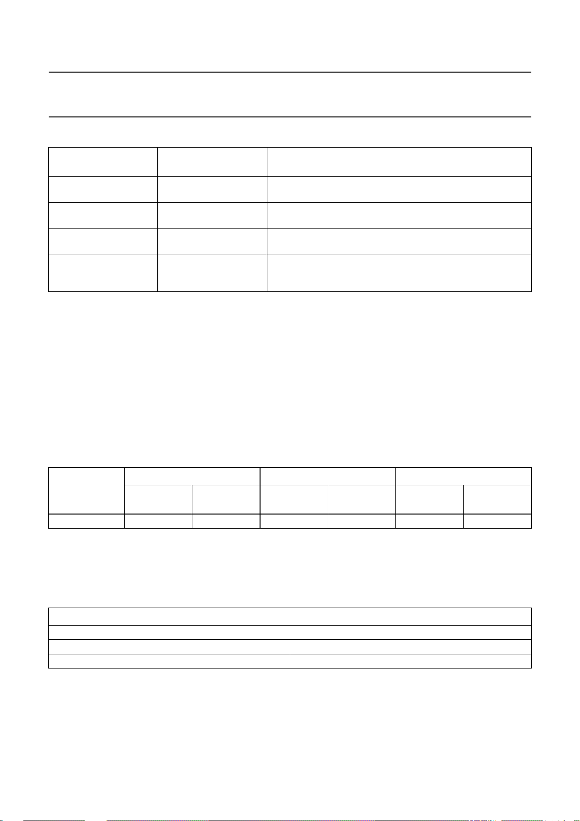
Table 13 Truth table for bits 7 and 8 on register#0 in write mode; conversion mode options; note 1
autoConvSelect
REGISTER#0 (7)
0 0 Default state: no auto channel incrementation, no A/D
1 0 Starts automatically an A/D conversion on the same channel
1 1 Starts automatically an A/D conversion on the next channel
0 1 No auto channel incrementation, no A/D conversion started
Note
1. The autoConvSelect bit has priority over the incrementChannel bit.
8.4.5 C
The ADC internal clock named converterClock can have two different frequency values by programming register#6 (11)
(bit highClock_N):
ONVERTER CLOCK FREQUENCY VALUES
incrementChannel
REGISTER#0 (8)
DESCRIPTION
conversion started automatically after each read of the result.
(no channel incrementation) after each read of the result.
(increment the channel by 1) after each read of the result.
automatically after each read of the result (similar to the default
state ‘00’).
Register#6 (11) = 1: means converterClock = Master clock (f
Register#6 (11) = 0: means converterClock = Master clock (f
conversionTime
Table 14 Numerical application
TIME
Conversion time 10.4 µs 5.2 µs 5.2 µs 2.6 µs 3.4 µs 1.7 µs
8.5 10-bit VCM DAC
The VCM DAC is a signed 10-bit digital-to-analog convertor. It will start the conversion when register#2 is written.
The lowest 10 bits contain the value to be converted.
Table 15 Input code and corresponding output analog voltage
13 clockDivider×
=
--------------------------------------------f
CLOCK
MASTER CLOCK = 10 MHz MASTER CLOCK = 20 MHz MASTER CLOCK = 30 MHz
DIVISION
BY 8
INPUT CODE OUTPUT VOLTAGE
200H 1.5 V
000H 2.5 V
1FFH 3.5 V
DIVISION
BY 4
DIVISION
BY 8
) divided by 8 (clockDivider = 8)
CLOCK
) divided by 4 (clockDivider = 4)
CLOCK
DIVISION
BY 4
DIVISION
BY 8
DIVISION
BY 4
(10)
The overall accuracy is 2% absolute error not including the contribution of the reference voltage and guaranteed
monotonicity.
1998 Nov 02 23
Page 24
Philips Semiconductors Product specification
Disk drive spindle and VCM with
servo controller
8.6 Reference voltage
V
is a 2.5 V bandgap reference used as the reference
ref2V5
voltage for the VCM circuit. Stable voltages of
1.5 and 3.5 V are generated from the 2.5 V reference and
used as reference voltages for the VCM DAC and for the
ADC. The 1.5 and 3.5 V voltages are only available inside
the IC and are not connected to external pins.
8.7 Stand-alone op-amps
This block is composed of two low-offset stand-alone
op-amps (A1 and A2) with outputs connected to the ADC
channels 0 and 1.
The stand-alone op-amps can be deactivated if they are
not used in the application. When deactivated, they are put
in sleep mode and outputs are in high-impedance. In that
case, ADC channels 0 and 1 can be used as input signals.
The op-amps are controlled by writing to the serial port on
register#0 (9); bit opampSelect_N:
Register#0 (9) = 0: means the op-amps are selected
and put in normal mode
Register#0 (9) = 1: means the op-amps are not selected
and put in sleep mode.
8.8 Analog switch
OM5193H
It is controlled by writing to serial port register#1 (9);
bit seek/trackfw:
Register#1 (9) = 0: means input SEEKSELECT is
selected and connected to VCMIN
Register#1 (9) = 1: means input TRACKFWSELECT is
selected and connected to VCMIN.
8.9 Charge pump voltage
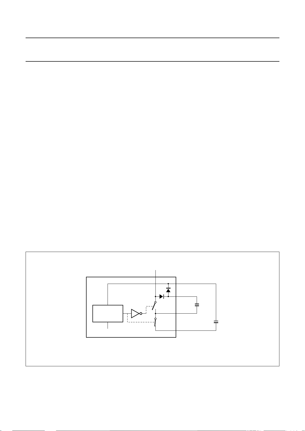
The charge pump voltage circuit (voltage doubler)
generates a power supply voltage higher than V
(12 V) power supply. This voltage is used to:
• Drive the upper N-channel FETs of the power stages
• Drive an optional external FET (see Section 8.18)
• Set a voltage independent of the power supply and
temperature for the functions BRAKEPOWER and
BRAKEDELAY.
Two external capacitors are used to generate the higher
voltage on pin CAPY. The capacitor between
BSTCP1 and BSTCP2 is charged and discharged with a
frequency, which is a function of the charge pump output
current and an internal oscillator frequency. The voltage
on pin CAPY is typically 19.2 V. Figure 10 illustrates the
charge pump block diagram.
DDA2
This block is composed of a 2 input analog multiplexer
used to select the seek mode or the track-following mode.
handbook, full pagewidth
COMPARATOR
OSCILLATOR
200 kHz
reference
Fig.10 Charge pump voltage generator.
V
DDA2
CAPY
BSTCP2
BSTCP1
GNDS
C
CAPX
MGM979
C
CAPY
1998 Nov 02 24
Page 25

Philips Semiconductors Product specification
Disk drive spindle and VCM with
servo controller
8.10 Spindle driver
The spindle block contains both the low-side and high-side
drivers configured as a H-bridge for a 3-phase DC
brushless, sensorless motor. In each of the six possible
states, two outputs are active, one sourcing current and
one sinking current. The third output presents a high
impedance to the motor which enables measurement of
the BEMF in the corresponding motor coil. The BEMF zero
crossing comparator outputs (xCROSS) are processed by
the commutation logic circuit to calculate the correct
moment for the next commutation, so the change to the
next output state. The commutation logic circuit provides
proper commutation commands for the spindle drivers
thus ensuring the rotation of the motor. The commutation
logic circuit also controls the spindle motor driver during
start-up (no reverse rotation).
The spindle should be set in the high-impedance mode
(see Table 16) between the sleep mode (brake-after-park
mode) and the normal running mode. Register#1 should
be programmed as follows:
• Write 00x001x11010 to activate the manual mode
during typically less than 1 ms (time discharge of
low-side power FETs)
• Write 00x001x01xxx to activate the automatic running
mode. The ‘x’ states concern the seek or track-following
mode register#1 (9) and the spindle prescaler value
used on the application register#1 (5). Their states are
specific to the application needs.
The ZCROSS signal is a combination of the xCROSS
signals. It can be used by the microcontroller as a tacho
information for the spindle speed control loop.
The external SPCC signal is used to control the spindle
current. The external SPCCOUT capacitor is connected to
the spindle current control amplifier to ensure the stability
of the spindle current control loop.
The short-circuit brake mode is entered if power-down,
thermal shutdown or sleep mode occurs.
A Miller network is used to obtain soft switching on the
low-side and high-side drivers.
The slew rate of the driver stage that is switched-off can be
controlled by means of a resistor connected to the pins
SLEW and GND. The slew rate is calculated using the
following equation:
20 pF
2.55
+()×
SLEW
(11)SR
3 µA
+
-------------------------------------------------------
=
---------------------------------------------------------------------------
41kΩR
OM5193H
is in Ω and SR in V/s. Without a resistor, SR is
R
SLEW
typical 0.15 V/µs and with a resistor of 90 kΩ, the typical
value is 0.5 V/µs. The maximum slew rate depends on the
limit for stability of the spindle loop.
The spindle current I
resistor R
SPSENSE
connected to a sense amplifier
providing the internal signal SPOUT. The gain Gv of the
sense amplifier is typical 10.
V
SPOUT
=
G
GvR
=
×
vVSPSENSEH
SPSENSEISPRUN
The transconductance gain of the spindle loop is given by
the following equation:
I
SPRUN
==
g
-------------------- -
s
V
SPOUT
=
----------------------------------------R
SPSENSEGv
1
---------------------------
R
SPSENSE
×
The control amplifier differentiates the control signal on
pin SPCC from the signal SPOUT. A 0.25 V offset is
subtracted from the input voltage on pin SPCC to ensure
that the current command includes the zero current. With
the spindle loop closed, the voltage SPOUT is given by the
following equation:
V
SPOUT
V
–=
SPCCVOFFSET
The control signal V
amplifier is then applied to the spindle drivers. The spindle
drivers control the voltage on the gate of the low-side
power drivers. One of the three high-side drivers is fully on.
The charge pump voltage is applied to the gate. One of the
three low-side drivers is controlled by the control amplifier.
Purpose is to adjust the voltage on the gate to adjust the
total output resistance R
current.
The current in the spindle loop is given by the following
formula:
I
SPRUN
With R
I
SPRUN
gsV
SPSENSE
0.4 V
SPCCVOFFSET
= 0.25 Ω:
The maximum start-up current is I
SPCC signal at 5 V.
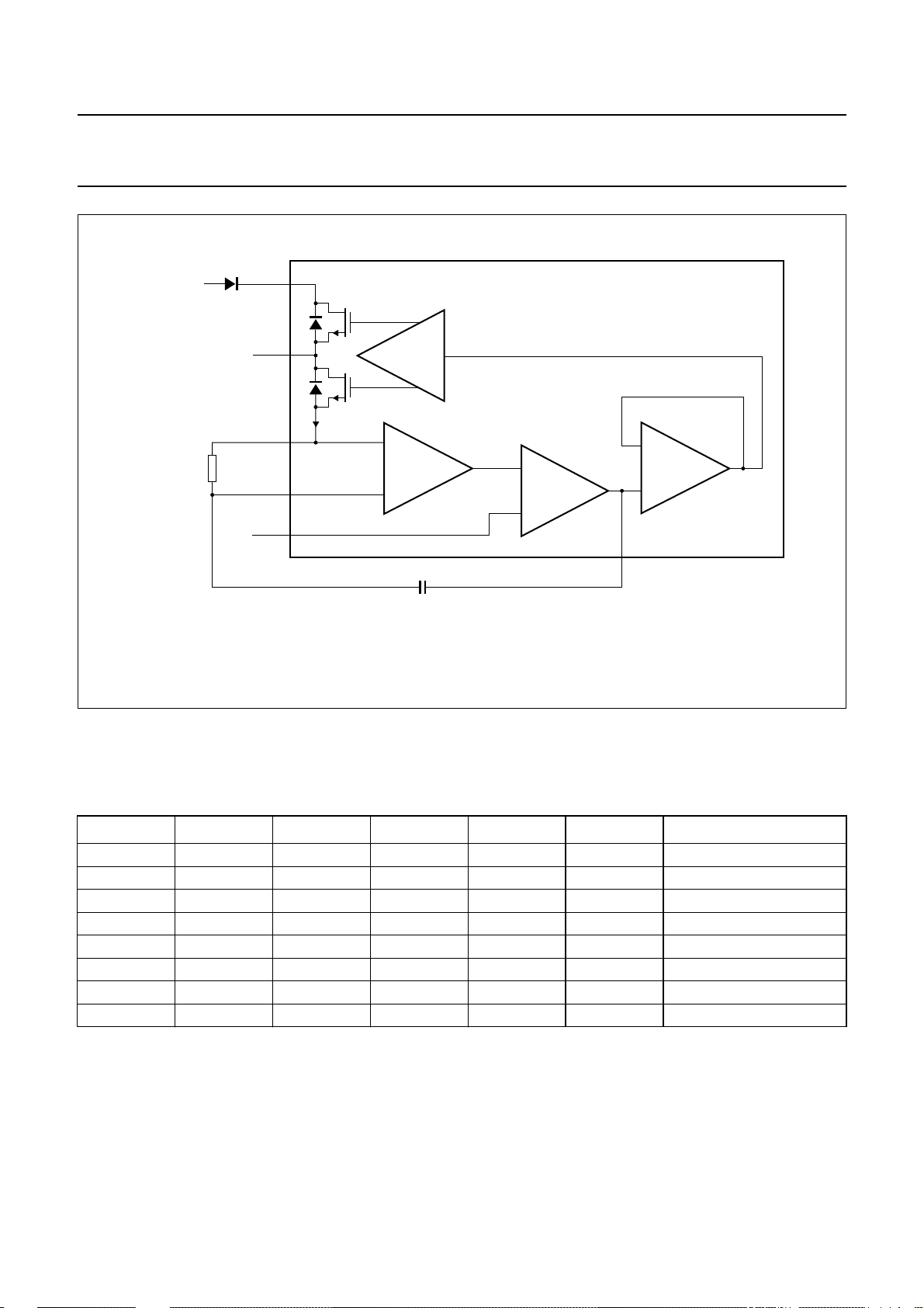
Figure 11 illustrates the spindle current control loop.
is sensed by an external
SPRUN
××
1
CONTROL
V
SPSENSEH
×
------------------------------ V
SPOUT
provided by the control
at the specified running
ds(on)
–()×=
SPCC
0.25–()×=
SPRUN
(12)
(13)
(14)
(15)
(16)
= 1.9 A with
1998 Nov 02 25
Page 26
Philips Semiconductors Product specification
Disk drive spindle and VCM with
servo controller
handbook, full pagewidth
V
DDA2POWER
R
SPSENSE
CLAMP
external
diode
MOTx
MOTSENSE/
SPSENSEH
GNDS/
SPSENSEL
SPCC
I
SPRUN
V
UPPER
V
LOWER
PREDRIVER
SENSE
AMPLIFIER
SPOUT
V
0.25 V
OFFSET
CONTROL
CONTROL
AMPLIFIER
SPCCOUT
OM5193H
MGM980
C
SPCCOUT
Fig.11 Spindle transconductance loop schematic.
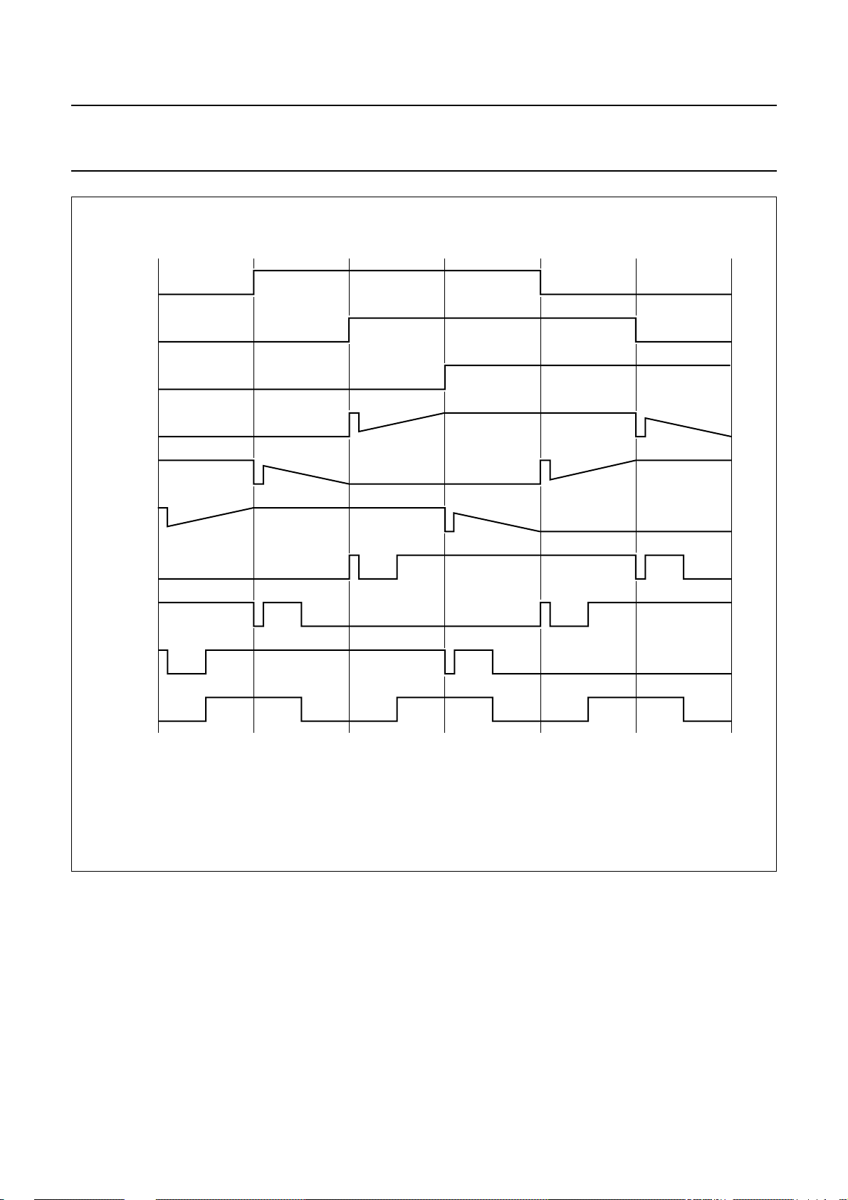
Table 16 and Fig.12 illustrate the relationship between the commutation signals and the associated output drivers and
output comparators.
Table 16 Input commutations to output drivers
COMA COMB COMC MOTA MOTB MOTC STATE
0 0 0 LOW HIGH float 1
1 0 0 LOW float HIGH 2
1 1 0 float LOW HIGH 3
1 1 1 HIGH LOW float 4
0 1 1 HIGH float LOW 5
0 0 1 float HIGH LOW 6
101F_L
(1)
F_L
(1)
F_L
(1)
SLEEP
0 1 0 float float float Spindle high-impedance
Note
1. F_L is for float-and-then-LOW (brake-after-park mode).
1998 Nov 02 26
Page 27
Philips Semiconductors Product specification
Disk drive spindle and VCM with
servo controller
handbook, full pagewidth
COMA 011100
COMB
COMC
MOTA
MOTB
MOTC
001110
000111
LL FHH
H
F
F
HH
LL
F
OM5193H
F
F
LL
H
ACROSS
BCROSS
CCROSS
ZCROSS
MGM981
L =LOW.
H =HIGH.
F =Floating.
Fig.12 Input commutations to output drivers.
8.11 VCM driver
The VCM driver is a linear, class AB amplifier with both low-side and high-side drivers configured as an H-bridge.
The zero-current reference voltage for the VCM loop is internally set at 2.5 V. The sense resistor R
VCM current (I
VCMRUN
The output voltage (V
) to be measured through the sense amplifier. The gain Gv of the sense amplifier is typically 4.
) on pin ADC[2]/SOUT is given by the following equation:
sout
VCMSENSE
enables the
V
sout
GvV
GvR
VCMSENSEIVCMRUNVref2V5
VCMSENSEHVVCMSENSEL
–()V
+××=
+×=
ref2V5
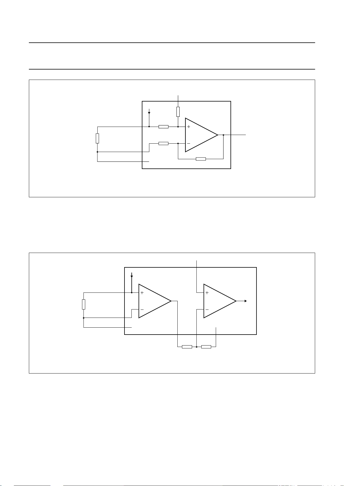
Figure 13 presents the VCM sense amplifier.
1998 Nov 02 27
(17)
Page 28
Philips Semiconductors Product specification
Disk drive spindle and VCM with
servo controller
handbook, full pagewidth
I
VCMRUN
VCMSENSEH
R
VCMSENSE
VCMSENSEL
NIVCM
R
R
Fig.13 VCM sense amplifier.
The error amplifier (see Fig.14) compares the DACOUT input command and the output signal V
to generate the control voltage of the power drivers.
REF2V5
4R
ADC[2]/SOUT
4R
MGM982
OM5193H
of the sense amplifier
sout
V
------------------------------------------------- -
handbook, full pagewidth
–
ref2V5VDACOUT
R
i
V
–
soutVref2V5
==
-------------------------------------- R
o
VCMSENSEH
R
VCMSENSE
VCMSENSEL
NIVCM
G
vRVCMSENSEIVCMRUN
---------------------------------------------------------------------------
I
VCMRUN
SENSE
AMPLIFIER
G
a
ADC[2]/SOUT
××
R
o
R
o
REF2V5
ERROR
AMPLIFIER
VCMIN DACOUT
R
i
Fig.14 VCM transconductance gain schematic.
Finally, the transconductance gain of the VCM loop is given by the following equation:
to power
drivers
MGM983
(18)
g
------------------------------------------------- -
v
V
ref2V5VDACOUT
I
VCMRUN
–
R
o
×==
---------------------------------------------
------ G
R
×
i
vRVCMSENSE
1
1998 Nov 02 28
(19)
Page 29

Philips Semiconductors Product specification
Disk drive spindle and VCM with
OM5193H
servo controller
The VCM loop gain is set through external resistors. The seek (high gain) or the track-following (low gain) mode is
controlled with the serial bus. Purpose is to set the appropriate gain by selecting the Ri resistor through the low
impedance analog 2 input switch.
handbook, full pagewidth
(1) High gain.
(2) Low gain.
R
i(SEEK)
ADC[2]/SOUT
SEEKSELECT
TRACKFWSELECT
R
i(TRACKFW)
DACOUT
R
(1)
(2)
VCM switch
VCM DAC
o
VCMIN
to VCM
drivers
MGM984
Fig.15 VCM selectable loop gain.
8.12 Park the VCM
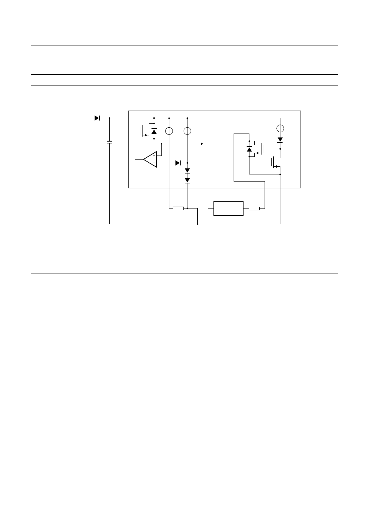
A VCM park sequence is initiated any time a power-down,
a thermal shutdown and/or a sleep mode situation occurs.
The fault signal (FAULT) initiates the VCM park sequence.
This secure function is accomplished even in case of
power loss. In this case, the energy provided by the
rectified BEMF of the spindle motor coils is used to supply
the park circuit and park the heads above a landing area.
Otherwise, the energy is provided by the V
DDA2
power
supply through an external diode or power FET.
To accomplish this function, the spindle power stage is
automatically set in a high-impedance mode. The NIVCM
low-side power driver is fully on while the remaining power
drivers of the VCM power stage are off.
The current flowing in the PARKVOLT resistor sets the
voltage on the PARKVOLT pin. The voltage across the
VCM load is internally regulated by the voltage on the
PARKVOLT pin. An internal circuit clamps the voltage on
PARKVOLT at 3V
PARKVOLT is 3VBE. The park current I
the VCM coil. The I
. Without resistor, the voltage on
BE
is applied to
coilpark
park current is given by the
coilpark
following equation:
V
coilpark
=
------------------------------------------------------------------------------------------R
VCMSENSERcoilRds on() ksin()
PARKVOLT
++
(20)I
An RC network is connected to pin BRAKEDELAY. During
the normal functioning, the voltage on the BRAKEDELAY
pin is typically V
= 12.55 V. This value is independent
BDC
of the power supply and the temperature. During park
mode, the RC network discharges with a time constant τ.
The park mode is activated as long as the voltage on the
BRAKEDELAY pin is greater than the internal brake delay
threshold voltage V
The t
park time duration (or brake delay time duration)
BDT
of typically 2.2 V.
BDT
is set by the following equation:
V
BDC
t
BDT
τ In
×=
------------V
BDT
(21)
where
τC
BRAKEDRBRAKED
BRAKED
and R
C
×=
BRAKED
are respectively the capacitor and
(22)
the resistor connected to the BRAKEDELAY pin.
Typically, with C
t
= 400 ms.
BDT
BRAKED
= 330 nF and R
BRAKED
= 650 kΩ,
Figure 16 shows the equivalent park circuit.
1998 Nov 02 29
Page 30
Philips Semiconductors Product specification
Disk drive spindle and VCM with
servo controller
handbook, full pagewidth
V
DDA2POWER
external
diode
C
CLAMP
CLAMP
PARKVOLT
R
PARKVOLT
I
coilpark
ACTUATOR
R
COIL
FAULT
NIVCMIVCM GNDVCMGNDV
R
VCMSENSE
OM5193H
MGM985
Fig.16 Park circuit.
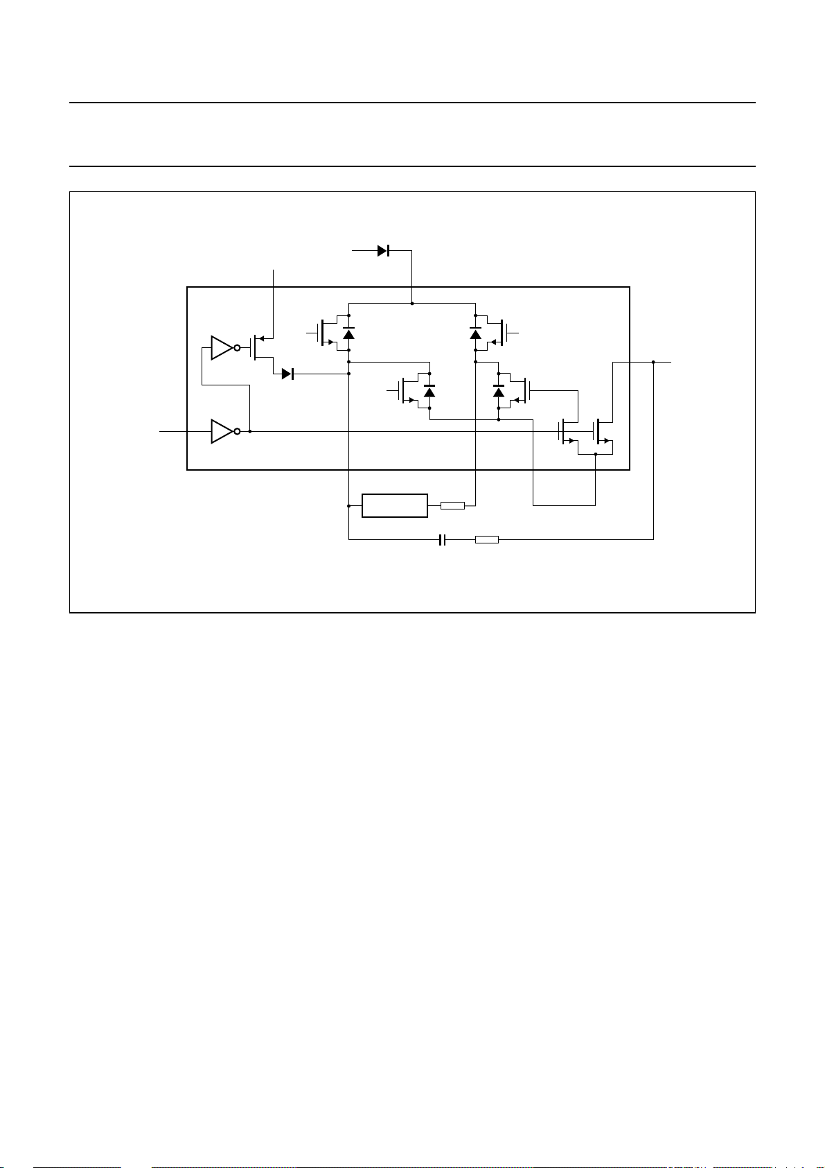
8.13 Precharge the VCM
When the voltage on the BRAKEDELAY pin goes below
the brake delay threshold voltage V
BDT
, the
BRAKEDELAY pin is short-circuited to ground. While the
brake mode is activated, the VCM outputs are precharged
to V
− VBE while pin VCMIN is short-circuited to
DDA1
ground.
This function precharges the external RC compensation
network.
The NIVCM low-side power driver is set off during VCM
precharge. This is convenient for actuators with a
magnetic latch.
The park circuit is powered off during VCM precharge with
the actuator latched.
1998 Nov 02 30
Page 31
Philips Semiconductors Product specification
Disk drive spindle and VCM with
servo controller
handbook, full pagewidth
BRAKEDELAY
V
DDA2POWER
V
DDA1
GND
external diode
GND
ACTUATOR
CLAMP
R
OM5193H
GND
VCMIN
NIVCMIVCM GNDVCM GNDV
VCMSENSE
Fig.17 Precharge circuit.
8.14 Brake the motor
A spindle brake sequence is initiated any time a
power-down, a thermal shutdown and/or a sleep mode
situation occurs. The fault signal activates the
brake-after-park sequence.
When the heads are parked, the motor has to be braked in
order to guarantee heads reliability. During the brake
sequence, the heads land on a dedicated area of the disk.
The OM5193H integrates a highly efficient, low cost brake
circuit. It is guaranteed to be functional in case of power
loss and thermal shutdown with a short time brake duration
thus minimizing friction of the heads on the landing zone.
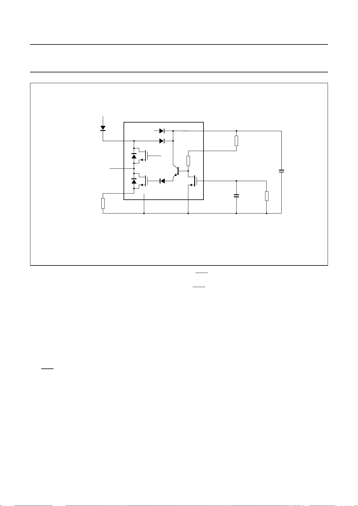
The energy stored by an external capacitor connected to
the BRAKEPOWER pin supplies the brake circuit during
the brake-after-park sequence.
The brake of the motor is accomplished by turning on the
spindle low-side power components while high-side power
drivers are off. This causes a short-circuit of the spindle
motor coils and thus reversing the current and torque of
the motor.
MGM986
During normal operation, the voltage V
BRAKEPOWER pin is typically V
BDC
on the
BDC
= 12.55 V. This value
is independent of the power supply and the temperature.
During the park sequence, the discharge of the
BRAKEPOWER capacitor is set by an internal resistor,
with or without an optional external resistor between
BRAKEPOWER and BRAKEADJUST. The typical value of
the internal resistor is 4 MΩ.
The brake sequence is started when the voltage on
BRAKEDELAY goes below the brake delay threshold
voltage V
of 2.2 V. The gates of the three spindle
BDT
low-side power drivers are charged by the energy stored in
the BRAKEPOWER capacitor and thus braking the motor.
The OM5193H will stay in the brake-after-park mode until
register#1 (3) bit run/stop is set to logic 1.
1998 Nov 02 31
Page 32
Philips Semiconductors Product specification
Disk drive spindle and VCM with
servo controller
handbook, full pagewidth
V
external
diode
R
SPSENSE
DDA2POWER
CLAMP
MOTx
MOTSENSE/
SPSENSEH
power-down
GND
GNDVGNDS/SPSENSEL
BRAKEPOWER
BRAKEADJH
BRAKEDELAY
C
BRAKED
R
BRAKEP
(optional)
R
BRAKED
C
BRAKEP
OM5193H
MGM987
Fig.18 Brake circuit.
The typical value for the BRAKEPOWER capacitor is 1 µF.
An optional resistance could be added between the
BRAKEPOWER and BRAKEADJUST pins. The values of
the capacitor and the resistor are depending on the
application.
Without resistor, the BRAKEADJH pin must be connected
to the BRAKEPOWER pin.
8.15 Power-on reset
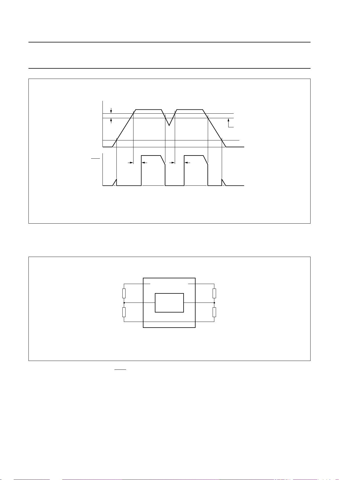
The Power-On Reset (POR) circuit monitors the voltage
level of both 5 and 12 V supply voltages as shown in
Fig.19.
POR active LOW logic line is set HIGH following the
The
5 and 12 V supply voltage rise above a specified voltage
threshold plus a hysteresis, and delayed by a time tC that
is determined by the external CPOR capacitor.
POR output remains HIGH until either the 5 or 12 V
This
supplies drop below their voltage threshold, at which point
the POR output becomes LOW.
The C
capacitor is charged with a typically 2.7 µA
CPOR
current. The voltage on CPOR is compared to the POR
circuit voltage reference of 2.55 V. The tC time is set by the
following equation:
C
t
------------------------------------------------=
C
where V
The value of the tC time is set by the C
×
CPORVPORREF
I
CPOR
PORREF
= 2.55 V and I
= 2.5 µA typically.
CPOR
CPOR
(23)
capacitor
value.
1998 Nov 02 32
Page 33
Philips Semiconductors Product specification
Disk drive spindle and VCM with
servo controller
handbook, full pagewidth
V
DD
0.8 V
POR
V
hys
t
C
Fig.19 Power-on reset timing.
OM5193H
MGM988
threshold
t
t
C
t
The values of the 5 and 12 V supply threshold voltages can be adjusted by adding external bridge resistors respectively
on the CHK5 and CHK12 pins. Internally, the CHK5 and CHK12 pins are designed as described in Fig.20.
handbook, halfpage
V
R
H5
R
L5
DDA1
CHK5
GNDS
POWER-ON
RESET
MGM989
V
DDA2
CHK12
R
R
H12
L12
Fig.20 CHK5 and CHK12 pins.
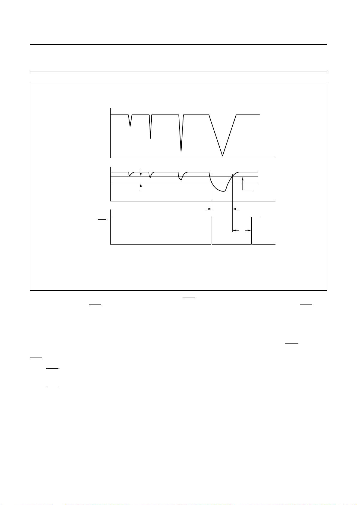
A glitch monitor prevents premature POR signals due to voltage spikes on power supplies. An external capacitor has to
be connected to the CHK5 and CHK12 pins to filter the noise on CHK5 and CHK12 pins caused by spikes on the power
supplies; see Fig.21.
1998 Nov 02 33
Page 34
Philips Semiconductors Product specification
Disk drive spindle and VCM with
servo controller
handbook, full pagewidth
V
DD
CHK signal
(with capacitor)
POR
∆V
minimum pulse
time = 10 µs
OM5193H
t
V
ref
t
t
C
MGM990
Fig.21 Glitch detector timing.
During a power-down situation, the POR circuit must not
only generate an outputPOR signal, but must also activate
the brake-after-park sequence. In doing so, the VCM
driver draws power from the BEMF of the motor coils
through the clamp line during spin-down, and uses this
power to bias the VCM against one of the hard stops of the
actuator. This prevents the heads from landing on data
zones.
POR also controls the digital part of the chip.
When POR is LOW, the chip is automatically set in the
brake-after-park mode.
When POR goes HIGH, the digital section is initialized
forcing the brake-after-park sequence until a normal start
is asked (by writing on register#1).
t
POR is considered as an asynchronous signal for the
digital part and default values are loaded when POR goes
HIGH. Default values for register#0 and register#1 are
shown in Section “Commutation and sleep mode” (see
also Table 5) and in Section “10-bit ADC with 7 analog
inputs” (see also Table 12).
If default values have to be loaded when POR is LOW, at
least one clock pulse is needed to load the registers with
default values.
1998 Nov 02 34
Page 35
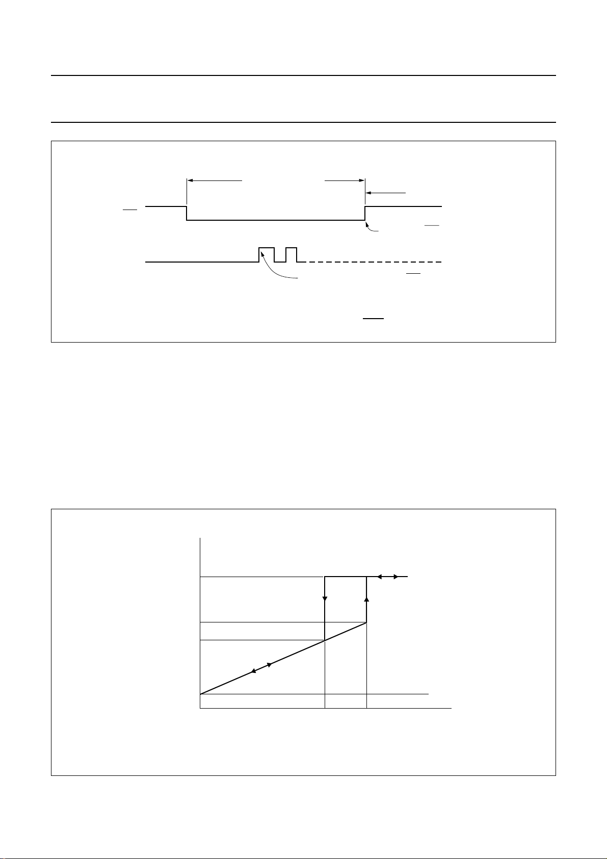
Philips Semiconductors Product specification
Disk drive spindle and VCM with
servo controller
handbook, full pagewidth
POR
CLOCK
Fig.22 Initialization of the registers when POR is LOW.
8.16 Thermal monitor and shutdown
The OM5193H is provided with both a temperature
monitor and a thermal shutdown circuit.
The device is protected against over-temperature by the
thermal shutdown circuit. When the temperature of the
chip exceeds 150 °C, the device is automatically set to the
brake-after-park mode. Furthermore, the voltage V
pin ADC[4]/TEMP goes HIGH. It remains in this mode until
the temperature goes below the thermal shutdown
temperature minus typically 10 °C.
POR circuit controls the
brake-after-park mode
on
temp
OM5193H
commutation logic controls the
brake-after-park mode until a
spindle start is asked.
default values are automatically
loaded when POR goes
HIGH if there is no CLOCK
during LOW state.
If there is a CLOCK signal when POR signal is LOW,
default register values will be loaded on the rising edge.
MGM991
During the normal operation, the signal V
voltage as a function of the chip temperature.
The equation of the voltage versus the temperature is the
following:
V
temp
Figure 23 presents the voltage V
7.05 103–× Tj°C()× 1.995+=
on pin ADC[4]/TEMP
temp
during normal operation and the voltage on thermal
shutdown with hysteresis.
provides a
temp
(24)
handbook, full pagewidth
V
temp
(V)
V
DDA1
3.052
2.982
1.995
0 140 150
Fig.23 V
behaviour versus temperature.
temp
1998 Nov 02 35
MGM992
Tj (°C)
Page 36

Philips Semiconductors Product specification
Disk drive spindle and VCM with
servo controller
The pin ADC[4]/TEMP is internally connected to channel 4
of the ADC. The data can be read and processed by the
microcontroller to control the temperature of the device
during the spindle start-up sequence and normal operation
and to create an early high-temperature warning.
8.17 Power supply isolation
In case of power-down, the brake-after-park sequence
must be supplied from the motor BEMF and the energy
stored in the CLAMP capacitor. When the supply voltage
for the spindle and the VCM is directly connected to the
V
, the energy from the motor BEMF and the CLAMP
DDA2
capacitor will be lost in the V supply system instead that it
is used for brake-after-park sequence. Therefore, the
motor and VCM supply must be isolated from the V
This can be done by means of a diode or a power FET
between V
and the power supply line for the spindle
DDA2
and the VCM.
8.17.1 E
XTERNAL ISOLATION DIODE
A diode can be used when the motor current and the VCM
current are low and the voltage drop over the diode does
not limit the supply voltage range of the motor and the
VCM. The diode can be either a normal diode or a
Schottky diode. The type and electrical properties of the
diode are determined by the load characteristics.
DDA2
OM5193H
The gate is connected to the SWITCHGATE pin. During
normal operation, the voltage on the SWITCHGATE pin is
about 19 V and the isolation transistor is conducting.
When the brake-after-park sequence is activated, the gate
is short-circuited to ground. The recirculation diode is used
to isolate the power supply from the power stages.
8.18 Thermal behaviour
The OM5193H uses a dedicated leadframe to effectively
drain the heat from the chip. Therefore 18 pins are
connected to the leadframe and called HEATSINK.
These pins must be short-circuited together and
connected to a large dissipating copper area on the
printed-circuit board. The copper area has to be as thick as
.
possible. The thermal resistance can also be decreased
by placing the device close to a mounting screw used to
fasten the printed-circuit board to the bare casting
assembly.
Paths used to connect the power stages to the external
components, ground and V
possible to guarantee a minimal extra thermal resistance
and a higher current capability.
must be as large as
DDA2
8.17.2 E
XTERNAL POWER FET
For higher current applications, the diode can be replaced
by a N-channel FET. The OM5193H contains an output to
drive this N-channel FET. To prevent the brake and park
currents from flowing back to V
must be connected to V
DDA2
, the source of the FET
DDA2
and the drain to the CLAMP
line. In this case, the back-gate diode of the FET is reverse
biased.
1998 Nov 02 36
Page 37

Philips Semiconductors Product specification
Disk drive spindle and VCM with
OM5193H
servo controller
9 LIMITING VALUES
In accordance with the Absolute Maximum System (IEC 134); note 1
SYMBOL PARAMETER MIN. MAX. UNIT
V
DDA1
V
DDD
V
DDA2
V
DDA2POWER
V
MOTA
V
MOTB
V
MOTC
V
NIVCM
V
IVCM
V
UB
V
es
T
amb
T
stg
T
j
5 V analog supply voltage −0.3 +6 V
5 V digital supply voltage −0.3 +6 V
12 V analog supply voltage −0.3 +13.5 V
output voltage −0.3 +18 V
output voltage −0.7 +18 V
voltage on pins BSTCP1, BSTCP2, CAPY and SWITCHGATE −0.3 +20.5 V
ESD Human Body Model − 2000 V
except for BRAKEDELAY − 500 V
except for BRAKEPOWER − 1500 V
ESD Machine Model − 200 V
operating ambient temperature 0 70 °C
storage temperature −55 +125 °C
junction temperature − 150 °C
Note
1. Stressing beyond these levels may cause permanent damage to the device. This is a stress rating only and functional
operation of the device under this condition is not implied.
a) OVS: one pin stressed by sample; square pulse time duration = 1 s, maximum current=1A.
b) ESD Human Body Model: JEDEC specification EIA/JESD22-A114 February 1996.
c) ESD Machine Model: JEDEC specification JC-14.1 July 07 1995.
10 HANDLING
Inputs and outputs are protected against electrostatic discharge in normal handling. However, to be totally safe, it is
desirable to take normal precautions appropriate to handling MOS devices.
11 THERMAL CHARACTERISTICS
SYMBOL PARAMETER CONDITIONS VALUE UNIT
R
th(j-a)
thermal resistance from junction to ambient note 1 26 K/W
Note
1. This is obtained with a thermally enhanced printed-circuit board tied to the bare casting assembly.
1998 Nov 02 37
Page 38
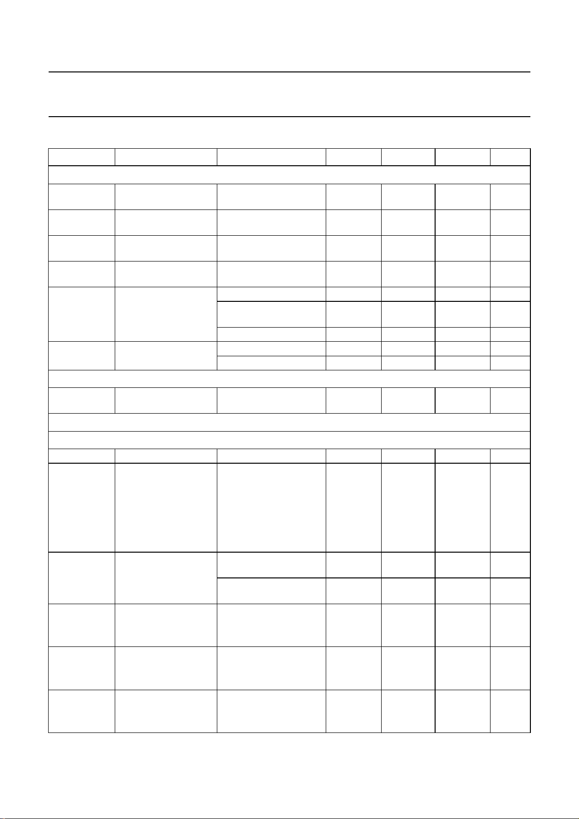
Philips Semiconductors Product specification
Disk drive spindle and VCM with
OM5193H
servo controller
12 CHARACTERISTICS
SYMBOL PARAMETER CONDITIONS MIN. TYP. MAX. UNIT
Supply; note 1
V
DDA1
V
DDD
V
DDA2
V
DDA2POWER
I
DDD
I
DDA2
OWER BIAS VOLTAGE
P
I
L(PWRBIAS)
5 V analog supply
voltage
5 V digital supply
voltage
12 V analog supply
voltage
12 V analog supply
voltage
5 V supply current normal mode − 40 70 mA
stand-alone op-amps
deactivated
sleep mode − 13mA
12 V supply current normal mode − 15 25 mA
sleep mode − 1.5 5 mA
power bias leakage
V
PWRBIAS
= 20.5 V −−200 nA
current
4.5 5.0 5.5 V
4.5 5.0 5.5 V
10.8 12.0 13.2 V
10.8 12.0 13.2 V
− 25 55 mA
Servo control; note 2
CHANNEL 10-BIT ADC
7
RES
t
CONV
V
I
OFF
E
i(max)
ADC
MID
resolution note 3 − 10 − bits
conversion time including the sample and
input voltage register#0 (6) = 0;
offsets for middle code analog input at V
input error for
maximum code
E
i(min)
input error for minimum
code
hold time; relative to
CLOCK signal
register#6 (11) = 0 −−104 clock
register#6 (11) = 1 −−52 clock
1.5 − 3.5 V
V
= 2.5 V
ref2V5
register#0 (6) = 1;
V
= 2.5 V
ref2V5
ref2V5
0 − 5V
1.5 to 3.5 V range −5 − +5 LSB
0 to 5 V range −7 − +7 LSB
relative to 1.4VI at 00H
1.5 to 3.5 V range −40 − +40 mV
0 to 5 V range −80 − +80 mV
relative to 0.6VI at 00H
1.5 to 3.5 V range −40 − +40 mV
0 to 5 V range −80 − +80 mV
cycles
cycles
1998 Nov 02 38
Page 39

Philips Semiconductors Product specification
Disk drive spindle and VCM with
OM5193H
servo controller
SYMBOL PARAMETER CONDITIONS MIN. TYP. MAX. UNIT
INL end-point integral non-
linearity
DNL differential non-linearity monotonic; no missing
CODE
C6
code value on
channel 6
E
C6
code error on
channel 6
E
absolute error includes integral
tot
R
i
C
i
input resistance 0 to 5 V range;
input capacitance 1.5 to 3.5 V range;
TC temperature coefficient combined temperature
CC
MATCH
channel-to-channel
matching
α
ct
crosstalk attenuation fi= 1 MHz; note 7 66 −−dB
PSRR power supply rejection
ratio
10-
BIT VCM DAC
RES
t
st
DR
DAC
V
OO(MID)
E
o(max)
E
o(min)
DAC
resolution − 10 − bits
settling time to within 0.5 LSB −−2.0 µs
dynamic range 0.6V
offsets for middle code measured at code 00H:
maximum output error relative to 1.4VO at
minimum output error relative to 0.6VO at
note 4
1.5 to 3.5 V range −4 − +4 LSB
0 to 5 V range −8 − +8 LSB
−1 − +1 LSB
codes; for both ranges;
note 4
1
⁄2V
(internal analog
DDA1
−190 − +190 LSB
value) is sampled and
converted in this channel
represents the
−30 − 0 LSB
difference between an
external1⁄2V
DDA1
conversion result and a
conversion made in
channel 6
−−2%
non-linearity, offset and
gain error
40 50 60 kΩ
notes 5 and 6
− 20 25 pF
note 6
coefficient of gain error,
integral non-linearity
and offset
T >25°C0−0.05 LSB/°C
T<25°C −0.05 − 0 LSB/°C
the same analog voltage
−−1 LSB
is applied in each
channel; note 6
note 6 50 −−dB
ref
2.5 (±1.0) 1.4V
ref
−10 − +10 mV
relative to V
ref2V5
−40 − +40 mV
code 00H
−40 − +40 mV
code 00H
V
1998 Nov 02 39
Page 40

Philips Semiconductors Product specification
Disk drive spindle and VCM with
OM5193H
servo controller
SYMBOL PARAMETER CONDITIONS MIN. TYP. MAX. UNIT
V
OO(max)
V
OO(min)
INL end-point integral
DNL differential non-linearity guaranteed monotonic;
E
absolute error includes integral
tot
TC temperature
PSRR power supply rejection
REFERENCE VOLTAGES
V
ref1V5
V
ref2V5
V
ref3V5
G
1V5
G
3V5
TC temperature coefficient note 6 −−200 µV/°C
PSRR power supply rejection
C
L
ANALOG SWITCH
t
sw
R
ds(on)
TC temperature coefficient T > 25 °C −−0.3 %/°C
I
L
maximum output offset
voltage
minimum output offset
voltage
relative to V
ref3V5(meas)
only tested on wafer
relative to V
ref1V5(meas)
only tested on wafer
;
−10 − +10 mV
;
−10 − +10 mV
note 4 −2 − +2 LSB
non-linearity
−1 − +1 LSB
note 4
−−2%
non-linearity, offset and
gain error
combined temperature
coefficient
coefficient of gain error,
integral non-linearity
and offset
T>25°C0−100 mV/°C
T<25°C −100 − 0 mV/°C
note 6 50 −−dB
ratio
1.5 V reference output
voltage
2.5 V reference output
0.6V
ref2V5(meas)
;
only tested on wafer
−1mA≤I
≤ 5 mA 2.397 2.507 2.617 V
ref
1.414 1.504 1.596 V
voltage
3.5 V reference output
voltage
value of the gain used
to generate V
ref1V5
1.4V
ref2V5(meas)
;
only tested on wafer
V
ref1V5(meas)
V
ref2V5(meas)
divided by
;
3.332 3.510 3.690 V
0.59 0.6 0.61 −
only tested on wafer
value of the gain used
to generate V
ref3V5
V
ref3V5(meas)
V
ref2V5(meas)
divided by
;
1.39 1.4 1.41 −
only tested on wafer
note 6 −−50 dB
ratio
load capacitance note 6 0.01 − 0.1 nF
switching time note 6 −−0.5 µs
total output resistance
(source + sink +
isolation)
switch closed; value at
25 °C and nominal
supply voltages
−−100 Ω
T<25°C −−−0.3 %/°C
off leakage current −−100 nA
1998 Nov 02 40
Page 41
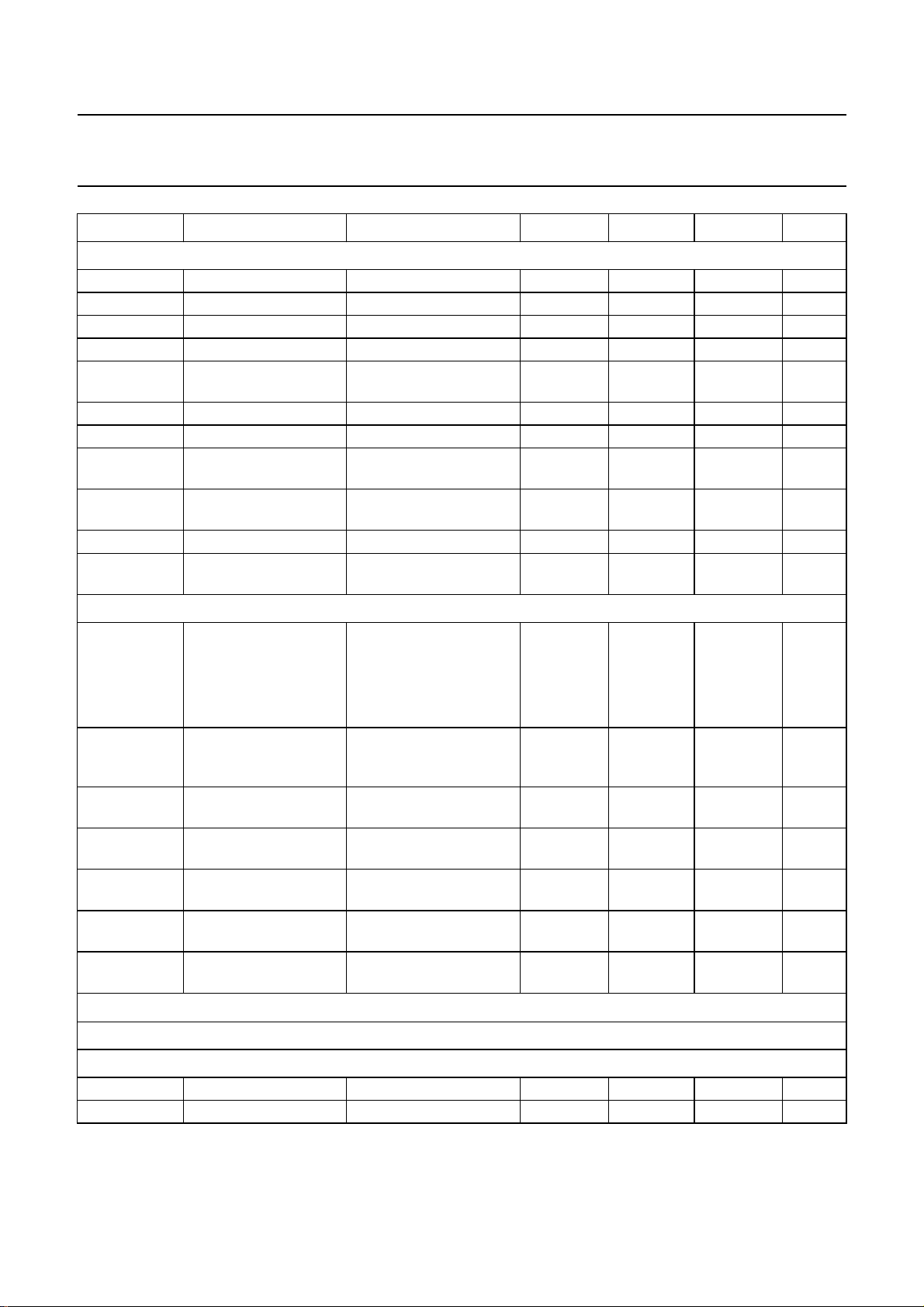
Philips Semiconductors Product specification
Disk drive spindle and VCM with
OM5193H
servo controller
SYMBOL PARAMETER CONDITIONS MIN. TYP. MAX. UNIT
STAND-ALONE OP-AMPS
V
I
I
i(bias)
V
IO
I
IO
V
O
SR slew rate R
GB gain bandwidth product 0.75 1.0 − MHz
G
v(ol)
SVRR supply voltage ripple
t
ON
CMRR common mode
D
IGITAL PINS
C
BIPIN
C
INPIN
C
OUTPIN
V
IH
V
IL
V
OH
V
OL
input voltage 1.4 − V
DDA1
− 0.5 V
input bias current −−1µA
input offset voltage relative to V
value −10 − +10 mV
ref2V5
input offset current note 6 −−100 nA
output voltage RL=10kΩ to V
ref2V5
0.9 − V
DDA1
− 0.5 V
level
=10kΩ; CL=20pF 5 −−V/µs
L
open-loop voltage gain f = 1 kHz; RL=10kΩ;
50 60 − dB
note 6
rejection
f = 100 kHz; R
CL< 20pF; note 6
=10kΩ;
L
60 70 − dB
power-on time after sleep mode −−1µs
note 6 60 70 − dB
rejection ratio
bidirectional pins
capacitance
CMOS level, high-drive,
output stage, 8 mA
3-state
input capacitance − 6 − pF
maximum output load −−100 pF
input pins capacitance CMOS level, high-drive,
protection to V
DDD
and
− 5 − pF
DGND
output pins
2 mA push-pull −−25 pF
capacitance
HIGH-level input
3 −−V
voltage
LOW-level input
−−0.8 V
voltage
HIGH-level output
IO=2mA V
− 0.5 −−V
DDA1
voltage
LOW-level output
IO=2mA −−0.5 V
voltage
Motor control; note 1
G
ENERAL
Thermal protection: thermal shutdown
T
sw(off)
hys
T
switch-off temperature note 8 143 150 157 °C
thermal hysteresis note 6 − 10 15 °C
1998 Nov 02 41
Page 42

Philips Semiconductors Product specification
Disk drive spindle and VCM with
OM5193H
servo controller
SYMBOL PARAMETER CONDITIONS MIN. TYP. MAX. UNIT
Thermal monitor
V
O(LT)
V
O(HT)
G
T
Charge pump generator: CAPY, BSTCP1 and BSTCP2
V
CP
V
SWITCHGATE
POWER-ON RESET
Power monitor comparators: CHK12 and CHK5
V
th(12)
V
hys(12)
V
th(5)
V
hys(5)
R
L12
R
H12
R
L5
R
H5
Power-on reset generator: CPOR and POR
V
OL
R
pu
I
CPOR(source)
V
th(CPOR)
SPINDLE DRIVER
output voltage at low
Tj=25°C − 2.171 − V
temperature
output voltage at high
Tj= 150 °C − 3.052 − V
temperature
temperature monitor
note 6 6.8 7.05 7.30 mV/°C
thermal gain
charge pump voltage running mode 18.2 19.2 20.2 V
switchgate voltage running mode 17.6 19 20 V
12 V threshold voltage CHK12 open-circuit 9.05 9.40 9.75 V
hysteresis on V
DDA2
80 115 150 mV
5 V threshold voltage CHK5 open-circuit 4.2 4.3 4.4 V
hysteresis on V
DDD
low internal bridge
resistor on CHK12
high internal bridge
resistor on CHK12
low internal bridge
resistor on CHK5
high internal bridge
resistor on CHK5
LOW-level output
CHK12 short-circuited to
2.55 V
CHK12 short-circuited to
ground
CHK5 short-circuited to
V
DDA1
CHK5 short-circuited to
ground
IOL=1mA −−0.5 V
35 50 70 mV
20 27.5 35 kΩ
60 80 100 kΩ
37 46 55 kΩ
24 32 40 kΩ
voltage
pull-up resistor POR short-circuited to
10 15 20 kΩ
ground
source current for
−3.5 −2.5 −1.5 µA
CPOR
CPOR threshold
functional test − 2.55 − V
voltage
BEMF comparators: ACROSS, BCROSS and CCROSS
V
I(CM)
common mode input
running mode −0.7 − V
voltage
I
I(bias)
input bias current note 6 −10 − 0 µA
1998 Nov 02 42
DDA2
+ 0.7 V
Page 43

Philips Semiconductors Product specification
Disk drive spindle and VCM with
OM5193H
servo controller
SYMBOL PARAMETER CONDITIONS MIN. TYP. MAX. UNIT
V
sw(comp)
V
sw(tol)
∆V
sw
V
i(hys)
V
OL
V
OH
Output drivers: MOTA, MOTB and MOTC
R
ds(on)(source)
R
ds(on)(sink)
V
SLEW
SR slew rate open-loop; note 9 0.09 − 0.23 V/µs
I
SPRUN
V
CLP
I
L(SP)
Sense amplifier: SPSENSEL and SPSENSEH
I
I
V
IO
G
v
TC temperature
Control amplifier: SPCC and SPCCOUT
V
SPCC0
comparator switching
only tested on wafer −20 − +20 mV
level
tolerance on the
only tested on wafer −3 − +3 mV
comparator switching
level
variation in comparator
note 6 −4.2 − +4.2 mV
switching levels for one
IC
input voltage
note 6 − 0.5 − mV
hysteresis
LOW-level output
voltage
HIGH-level output
voltage
high-side driver output
resistance
low-side driver output
resistance
slew rate voltage I
spindle current control V
overvoltage protection
sink current = −40 µA;
−−0.45 V
only tested on wafer
source current = 40 µA;
V
− 0.5 −−V
DDA1
only tested on wafer
IO= 1.0 A at
T
=25°C
amb
= 1.0 A at
I
O
T
= 125 °C
amb
IO= 1.0 A at
T
=25°C
amb
I
= 1.0 A at
O
T
= 125 °C
amb
=20µA − 2.55 − V
SLEW
I
=30µA; note 9 0.32 − 0.87 V/µs
SLEW
= 1.25 V;
SPCC
R
I
SVDMOS
= 0.25 Ω
SENSE
>10mA − 15.8 − V
− 0.36 0.45 Ω
− 0.56 0.65 Ω
− 0.24 0.35 Ω
− 0.44 0.55 Ω
380 400 420 mA
circuit
spindle power stage
−−1mA
leakage current
input current on
only tested on wafer 10 − 10 µA
MOTSENSE
input offset voltage note 6 − 3 − mV
sense amplifier gain only tested on wafer 9.8 10 10.2 V/V
note 6 − 200 − ppm/°C
coefficient of sense
amplifier gain
spindle zero-current
reference
only tested on wafer;
T
=25°C
amb
230 250 270 mV
1998 Nov 02 43
Page 44
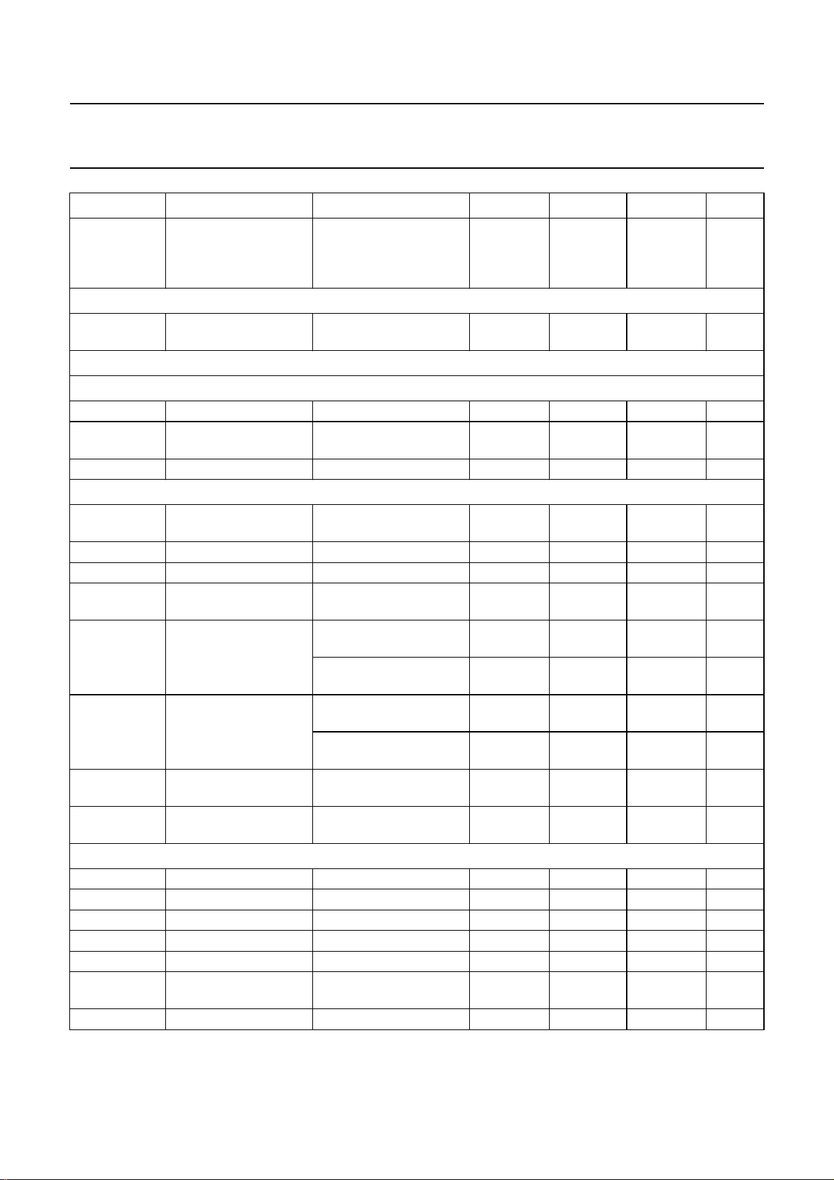
Philips Semiconductors Product specification
Disk drive spindle and VCM with
OM5193H
servo controller
SYMBOL PARAMETER CONDITIONS MIN. TYP . MAX. UNIT
f
cut(ol)
Logic decoder: COMA, COMB and COMC
I
LI
VOICE COIL MOTOR DRIVER
VCM preamplifiers: VCMIN and REF2V5
I
I
V
IO
f
G
VCM driver amplifiers
t
COD
SR
VCM
f
G
G
v(SD)
R
ds(on)(source)
R
ds(on)(sink)
V
CLP
I
LI(VCM)
VCM sense amplifier: VCMSENSEL and VCMSENSEH
V
I
I
I
G
v
I
O(sink)
I
O(source)
V
OO
GB gain-bandwidth product note6 5 8 − MHz
open-loop cut-off
frequency at 0 dB
C
SPCCOUT
minimum
value = 10 nF for stability
−−3 kHz
when closed loop;
note 10
input leakage current VI= 0 to VDD; only tested
−1 − +1 µA
on wafer
input current on VCMIN 1 − 0 µA
input offset voltage relative to V
ref2V5
for zero
−10 − +10 mV
output current
unity gain frequency note 6 2 3.5 − MHz
cross-over distortion
note 6 − 35µs
delay
VCM slew rate CL= 10 pF; note 6 − 1 − V/µs
unity gain frequency note 6 1.5 −−MHz
slave driver voltage
1.05 1.15 1.25
gain
high-side driver output
resistance
low-side driver output
resistance
overvoltage protection
IO= 1.0 A at
T
=25°C
amb
I
= 1.0 A at
O
T
= 125 °C
amb
IO= 1.0 A at
T
=25°C
amb
I
= 1.0 A at
O
T
= 125 °C
amb
I
SVDMOS
>10mA − 15.1 − V
− 0.45 0.55 Ω
− 0.65 0.75 Ω
− 0.35 0.45 Ω
− 0.55 0.65 Ω
circuit
VCM power stage
−−1mA
leakage current
input voltage −0.7 − V
input current V
= 2.5 V −100 − +250 µA
ref2V5
DDA2
+ 0.7 V
sense amplifier gain under all conditions 3.8 4.0 4.2
output sink current Tj= 0 to 140 °C; note 11 600 −−µA
output source current Tj= 0 to 140 °C; note 12 −−−500 µA
output offset voltage V
VCMSENSEH
V
VCMSENSEL
=
=6V
−15 10 +35 mV
1998 Nov 02 44
Page 45

Philips Semiconductors Product specification
Disk drive spindle and VCM with
OM5193H
servo controller
SYMBOL PARAMETER CONDITIONS MIN. TYP. MAX. UNIT
SR slew rate RL=10kΩ; CL= 60 pF;
note 6
G
v(ol)
SVRR supply voltage ripple
CMRR common mode
open-loop voltage gain note 6 75 80 − dB
rejection
f = 100 Hz; R
CL< 60 pF; note 6
=10kΩ;
L
note 6 90 −−dB
rejection ratio
B
RAKE-AFTER-PARK DELAY MODE
Park and brake power
V
NMBP
normal mode voltage
on brake power
V
NMBD
normal mode voltage
on brake delay
I
BPR
I
BPB
brake power park
current
brake power brake
current
V
BRAKEPOWER
V
BRAKEDELAY>VBDT
V
BRAKEPOWER
V
BRAKEDELAY
=12V;
=12V;
=0
Park
V
SWITCHGATE
voltage on
brake-after-park mode −−0.1 V
SWITCHGATE during
brake-after-park
I
brake
V
IVCM(max)
park voltage current
source
V
BRAKEPOWER
V
V
=8V;
CLAMP
BRAKEDELAY>VBDT
maximum park voltage pin PARKVOLT
=12V;
open-circuit;
V
IVCM(park)
V
NIVCM(park)
V
MOTx(park)
voltage on IVCM during
park
voltage on NIVCM
during park
voltage on MOTx
during park (high
V
V
T
V
V
V
V
V
V
V
V
V
note 14
=8V;
CLAMP
BRAKEDELAY>VBDT
=25°C; note 13
amb
PARKVOL T
BRAKEPOWER
CLAMP
BRAKEDELAY>VBDT
PARKVOLT
BRAKEPOWER
CLAMP
BRAKEDELAY>VBDT
BRAKEDELAY>VBDT
=1V;
=12V;
=8V;
=1V;
=12V;
=8V;
impedance state)
R
ds(on)(park)
TC
Rds(on)(park)
switch park resistor RL= 20.2 Ω;
T
=25°C
amb
temperature coefficient note 15 − 2 − mΩ/°C
1.7 − 5.3 V/µs
90 100 − dB
12.0 12.55 12.9 V
12.0 12.55 12.9 V
135µA
−−1µA
−12 −9 −6 µA
− 1.95 − V
;
0.9 1 1.1 V
− 15 50 mV
;
369V
− 0.35 2 Ω
1998 Nov 02 45
Page 46
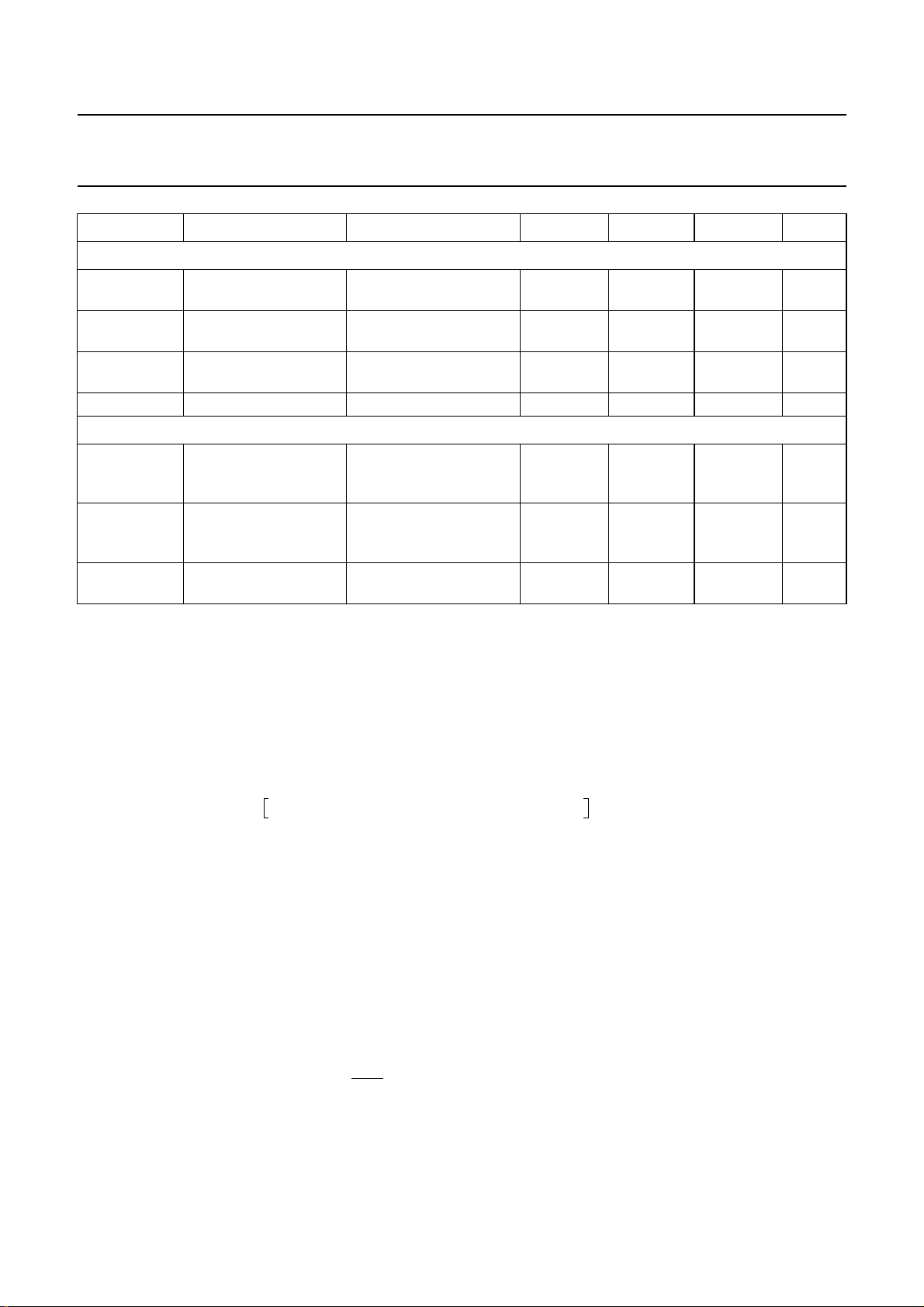
Philips Semiconductors Product specification
Disk drive spindle and VCM with
OM5193H
servo controller
SYMBOL PARAMETER CONDITIONS MIN. TYP. MAX. UNIT
Brake
V
BDT
I
LI
R
ds(on)(brake)
TC
Rds(on)(brake)
Precharge
V
IVCM
V
NIVCM
V
VCMIN
Notes
1. V
2. V
=5V±10%; V
DDD
DDD=VDDA1
3. LSB on the 1.5 to 3.5 V range is equal to
4. Integral non-linearity means the deviation of a code from a straight line passing through an actual end-point and the
actual centre. INL and DNL are calculated by dividing the output transfer function in 2 parts: minimum value to centre
value and centre value to maximum value.
5. The temperature dependency of the resistance is expressed as follows:
Rsh(T) RshT
where R
T = desired temperature and T
6. Guaranteed by design.
7. Channel-to-channel crosstalk is measured while driving one input and measuring the other open inputs.
8. In any case, it allows to go beyond the rated 150 °C limit.
9. The description of the spindle driver circuit is given in Section 8.10.
10. R
SENSE
series with a resistor RS= 3.2 Ω. Guaranteed by design.
11. V
VCMSENSEL
12. V
VCMSENSEL
13. V
PARKVOLT(max)
14. Brake-after-park mode when in sleep, POR or over-temperature mode.
15. R
ds(on)T(park)=Rds(on)(park)+TRds(on)(park)
16. R
ds(on)T(break)=Rds(on)(break)+TRds(on)(break)
17. VBE= 0.65 + 2e − 3 × (T − 25).
brake delay time
V
BRAKEPOWER
= 12 V 1.1 2.1 3.1 V
threshold voltage
brake delay leakage
−500 − +500 nA
current
lower DMOS resistor
during a brake
I
MOTx
T
amb
= 200 mA;
=25°C
− 0.24 0.5 Ω
temperature coefficient note 16 − 2 − mΩ/°C
voltage on pin IVCM V
BRAKEPOWER
V
BRAKEDELAY
=12V;
=0;
− V
− VBE− V
DDD
note 17
voltage on pin NIVCM V
BRAKEPOWER
V
BRAKEDELAY
=12V;
=0;
− V
− VBE− V
DDD
note 17
voltage on pin VCMIN V
DDA2=VDDA2POWER
=5V±10%; T
() 1(1.1e+ 3TT
ref
(T) = resistance at desired temperature; Rsh(T
sh
= 0 to 70 °C.
amb
ref
V
=27°C.
BRAKEPOWER
BRAKEDELAY
=12V±10%; T
1
⁄
512
–()+1.1e6 TT
=12V;
−−0.2 V
=0
= 0 to 70 °C; unless otherwise specified.
amb
V; LSB on the 0 to 5 V range is equal to
2
–()
ref
×–×–×=
) = resistance at reference temperature;
ref
ref
2.5
⁄
512
V.
= 0.25 Ω. Model for a motor phase: RLC network in parallel (LP= 1.5 mH, CP= 100 pF, RP= 4.6 kΩ) in
= 0.4 V, V
= 0 V, V
=3×VBE, V
VCMSENSEH
VCMSENSEH
= 0 V, measured V
= 0.4 V, measured V
PARKVOLT
=3×0.70 − 3 × 2e − 3 × (T − 25) without resistor.
sout=VO
sout=VO
, force V
, force V
sout=VO
sout=VO
+ 10 mV.
−10 mV.
× (T − 25).
× (T − 25).
1998 Nov 02 46
Page 47
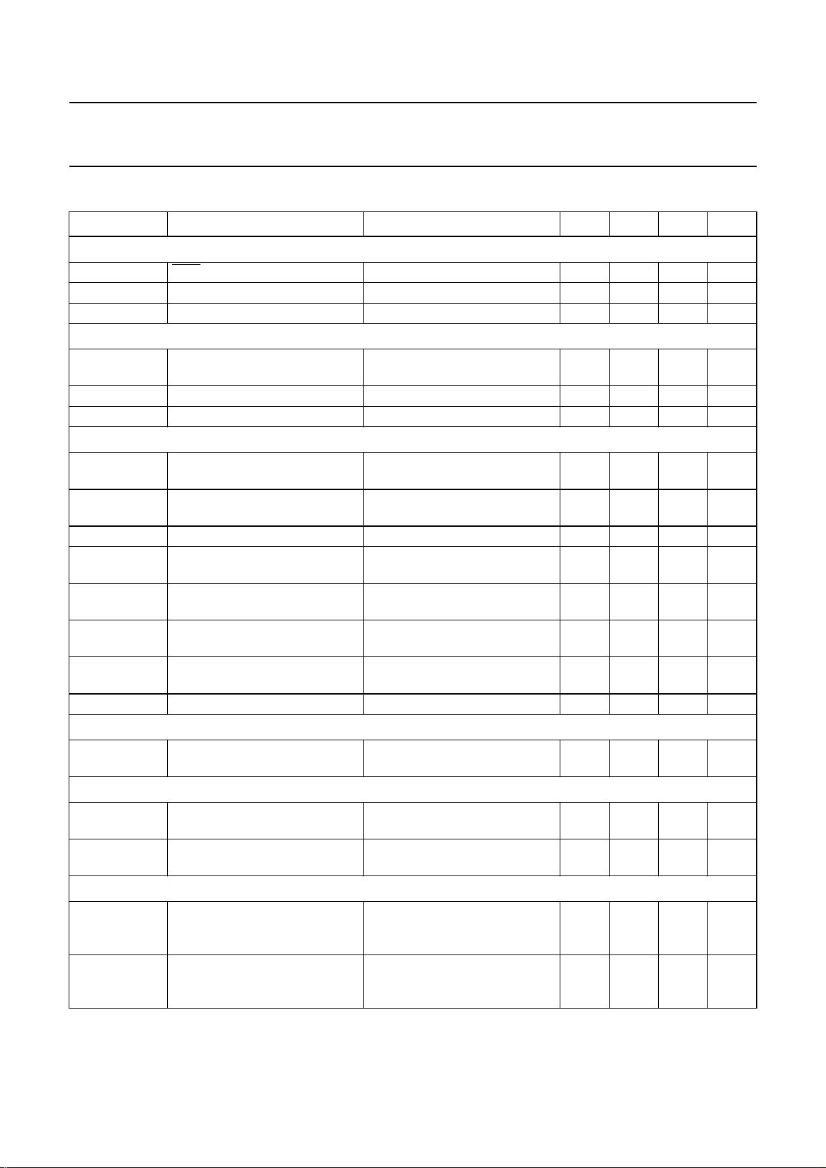
Philips Semiconductors Product specification
Disk drive spindle and VCM with
OM5193H
servo controller
13 APPLICATION INFORMATION
SYMBOL PARAMETER CONDITIONS MIN. TYP. MAX. UNIT
Power supplies monitor
C
CPOR
C
CHK5
C
CHK12
Spindle driver
C
SPCCOUT
R
SLEW
R
SPSENSE
VCM driver
R
VCMCOMPRC
C
VCMCOMPRC
R
VCMSENSE
R
FEEDBACK
R
VCMSEEK
R
VCMTRACKFW
V
I
V
ref2V5
Clamp line
C
CLAMP
POR time capacitor (time tC) note 1 − 100 − nF
analog 5 V filter between CHK5 and ground − 1 − nF
analog 12 V filter between CHK12 and ground − 1 − nF
spindle current control loop
capacitor
function of the motor
characteristics
− 10 − nF
slew up and down resistor note 2 − 200 − kΩ
spindle sense resistor − 0.25 −Ω
resistor of compensation
RC network
capacitor of compensation
RC network
function of the VCM
characteristics
function of the VCM
characteristics
− 130 − kΩ
− 1 − nF
VCM sense resistor − 0.33 −Ω
feedback resistor function of the VCM
− 2.67 − kΩ
characteristics
seek mode resistor function of the VCM
− 2.43 − kΩ
characteristics
track-following mode resistor function of the VCM
− 10 − kΩ
characteristics
input voltage controlling the
1.5 − 3.5 V
current
2.5 V reference voltage − 2.5 − V
clamp capacitor between
− 1 −µF
CLAMP line and ground
Charge pump generator
C
CAPX
pump capacitor between
pins BSTCP1 and BSTCP2
C
CAPY
storage capacitor between
pin CAPY and ground
Park and brake functions
C
BRAKEP
BRAKEPOWER capacitor brake time = 10 s;
speed = 5400 RPM;
R
=5Ω; BEMF = 8.2 V
coil
R
BRAKEP
resistor between BRAKEADJH
and BRAKEPOWER
brake time = 10 s;
speed = 5400 RPM;
R
=5Ω; BEMF = 8.2 V
coil
1998 Nov 02 47
− 10 − nF
− 22 − nF
− 1 −µF
− 0 − MΩ
Page 48

Philips Semiconductors Product specification
Disk drive spindle and VCM with
OM5193H
servo controller
SYMBOL PARAMETER CONDITIONS MIN. TYP. MAX. UNIT
C
BRAKED
R
BRAKED
R
PARKVOLT
Notes
1. The description of the Power-On Reset (POR) circuit is given in Section “Power-on reset”.
2. The description of the spindle driver circuit is given in Section “Spindle driver”.
BRAKEDELAY capacitor brake delay = 400 ms − 330 − nF
BRAKEDELAY resistor brake delay = 400 ms − 650 − kΩ
PARKVOLT resistor V
PARKVOLT
V
CLAMP
= 1.25 V;
=8V
− 250 − kΩ
1998 Nov 02 48
Page 49
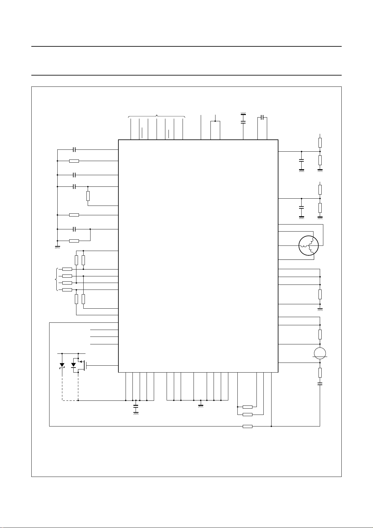
Philips Semiconductors Product specification
Disk drive spindle and VCM with
servo controller
handbook, full pagewidth
C
CPOR
R
SLEW
(1)
C
SPCCOUT
C
BRAKEP
R
BRAKEP
R
PARKVOLT
(1)
C
BRAKED
R
BRAKED
read
channel
V
DDA2POWER
two different
options
CPOR
SLEW
SPCCOUT
BRAKEPOWER
(1)
BRAKEADJH
PARKVOLT
BRAKEDELAY
REF2V5
INTIN
INTINN
PESAMP
PESAMPN
ADC[0]/INTOUT
ADC[1]/DIFOUT
ADC[2]/SOUT
ADC[3]
ADC[4]/TEMP
ADC[5]
SWITCHGATE
45
12
14
48
49
51
50
40
38
37
36
35
28
29
30
31
32
33
8
10
CLAMP155CLAMP256CLAMP3
microcontroller
CLOCK24SPCC13SDEN21SDATA22SCLOCK23POR
57
PWRBIAS1
C
CLAMP
77
39
AGND
PWRBIAS2
19
27
DGND
ZCROSS
25
OM5193H
1, 4 to 7,
58 to 61,
64 to 67,
70, 75,
78 to 80
54
GNDV
12 V 5 V
DDA2
V
15
26
HEATSINK
SCANTEST
R
VCMTRACKFW
DDD
V
V
20
44
71
GNDVCM1
R
VCMSEEK
C
CAPY
DDA1
68
63
GNDVCM2
GNDVCM3
CAPY
18
34
DACOUT
R
FEEDBACK
C
CAPX
BSTCP116BSTCP2
17
46
47
9
72
74
3
73
76
2
11
69
53
52
62
41
42
43
VCMIN
SEEKSELECT
TRACKFWSELECT
OM5193H
CHK5
C
CHK5
R
CHK12
C
CHK12
CT
MOTA
MOTB
MOTC
MOTSENSE3
MOTSENSE2
MOTSENSE1/
SPSENSEH
GNDS/SPSENSEL
NIVCM
VCMSENSEL
VCMSENSEH
IVCM
R
C
R
R
SPSENSE
R
VCMSENSE
voice
coil
motor
VCMCOMPRC
VCMCOMPRC
MGM993
R
R
H12
H5
L12
L5
5 V
12 V
spindle
motor
M
(1)
(1)
(1)
(1)
(1) Optional components.
Fig.24 Application diagram.
1998 Nov 02 49
Page 50
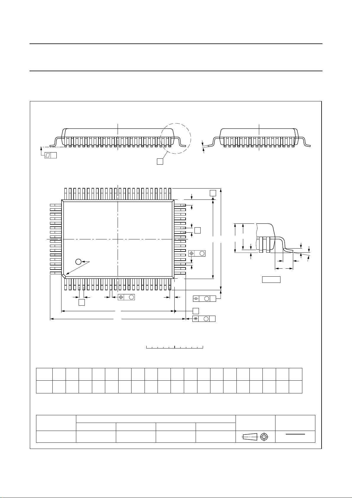
Philips Semiconductors Product specification
Disk drive spindle and VCM with
servo controller
14 PACKAGE OUTLINE
QFP80: plastic quad flat package; 80 leads (lead length 1.95 mm); body 14 x 20 x 2.8 mm
c
y
X
64 41
65
40
A
Z
E
OM5193H
SOT318-2
pin 1 index
80
1
w M
b
0.25
0.45
0.30
p
D
H
D
0 5 10 mm
(1)
(1) (1)(1)
D
0.25
0.14
20.1
19.9
14.1
13.9
e
DIMENSIONS (mm are the original dimensions)
mm
A
max.
3.2
0.25
0.05
2.90
2.65
UNIT A1A2A3bpcE
Note
1. Plastic or metal protrusions of 0.25 mm maximum per side are not included.
24
Z
D
scale
eH
H
24.2
0.8 1.95
23.6
25
D
e
w M
b
p
B
E
18.2
17.6
H
E
v M
A
v M
B
LL
p
1.0
0.6
A
2
A
E
A
1
0.20.2 0.1
detail X
Z
D
1.0
0.6
Zywv θ
1.2
0.8
(A )
3
θ
L
p
L
E
o
7
o
0
OUTLINE
VERSION
SOT318-2
IEC JEDEC EIAJ
REFERENCES
1998 Nov 02 50
EUROPEAN
PROJECTION
ISSUE DATE
95-02-04
97-08-01
Page 51

Philips Semiconductors Product specification
Disk drive spindle and VCM with
servo controller
15 SOLDERING
15.1 Introduction
There is no soldering method that is ideal for all IC
packages. Wave soldering is often preferred when
through-hole and surface mounted components are mixed
on one printed-circuit board. However, wave soldering is
not always suitable for surface mounted ICs, or for
printed-circuits with high population densities. In these
situations reflow soldering is often used.
This text gives a very brief insight to a complex technology.
A more in-depth account of soldering ICs can be found in
our
“Data Handbook IC26; Integrated Circuit Packages”
(order code 9398 652 90011).
15.2 Reflow soldering
Reflow soldering techniques are suitable for all QFP
packages.
The choice of heating method may be influenced by larger
plastic QFP packages (44 leads, or more). If infrared or
vapour phase heating is used and the large packages are
not absolutely dry (less than 0.1% moisture content by
weight), vaporization of the small amount of moisture in
them can cause cracking of the plastic body. For details,
refer to the Drypack information in the
IC26; Integrated Circuit Packages; Section: Packing
Methods”
Reflow soldering requires solder paste (a suspension of
fine solder particles, flux and binding agent) to be applied
to the printed-circuit board by screen printing, stencilling or
pressure-syringe dispensing before package placement.
.
“Data Handbook
OM5193H
If wave soldering cannot be avoided, for QFP
packages with a pitch (e) larger than 0.5 mm, the
following conditions must be observed:
• A double-wave (a turbulent wave with high upward
pressure followed by a smooth laminar wave)
soldering technique should be used.
• The footprint must be at an angle of 45° to the board
direction and must incorporate solder thieves
downstream and at the side corners.
During placement and before soldering, the package must
be fixed with a droplet of adhesive. The adhesive can be
applied by screen printing, pin transfer or syringe
dispensing. The package can be soldered after the
adhesive is cured.
Maximum permissible solder temperature is 260 °C, and
maximum duration of package immersion in solder is
10 seconds, if cooled to less than 150 °C within
6 seconds. Typical dwell time is 4 seconds at 250 °C.
A mildly-activated flux will eliminate the need for removal
of corrosive residues in most applications.
15.4 Repairing soldered joints
Fix the component by first soldering two diagonallyopposite end leads. Use only a low voltage soldering iron
(less than 24 V) applied to the flat part of the lead. Contact
time must be limited to 10 seconds at up to 300 °C. When
using a dedicated tool, all other leads can be soldered in
one operation within 2 to 5 seconds between
270 and 320 °C.
Several methods exist for reflowing; for example,
infrared/convection heating in a conveyor type oven.
Throughput times (preheating, soldering and cooling) vary
between 50 and 300 seconds depending on heating
method. Typical reflow peak temperatures range from
215 to 250 °C.
15.3 Wave soldering
Wave soldering is not recommended for QFP packages.
This is because of the likelihood of solder bridging due to
closely-spaced leads and the possibility of incomplete
solder penetration in multi-lead devices.
CAUTION
Wave soldering is NOT applicable for all QFP
packages with a pitch (e) equal or less than 0.5 mm.
1998 Nov 02 51
Page 52

Philips Semiconductors Product specification
Disk drive spindle and VCM with
OM5193H
servo controller
16 DEFINITIONS
Data sheet status
Objective specification This data sheet contains target or goal specifications for product development.
Preliminary specification This data sheet contains preliminary data; supplementary data may be published later.
Product specification This data sheet contains final product specifications.
Limiting values
Limiting values given are in accordance with the Absolute Maximum Rating System (IEC 134). Stress above one or
more of the limiting values may cause permanent damage to the device. These are stress ratings only and operation
of the device at these or at any other conditions above those given in the Characteristics sections of the specification
is not implied. Exposure to limiting values for extended periods may affect device reliability.
Application information
Where application information is given, it is advisory and does not form part of the specification.
17 LIFE SUPPORT APPLICATIONS
These products are not designed for use in life support appliances, devices, or systems where malfunction of these
products can reasonably be expected to result in personal injury. Philips customers using or selling these products for
use in such applications do so at their own risk and agree to fully indemnify Philips for any damages resulting from such
improper use or sale.
1998 Nov 02 52
Page 53

Philips Semiconductors Product specification
Disk drive spindle and VCM with
servo controller
OM5193H
NOTES
1998 Nov 02 53
Page 54

Philips Semiconductors Product specification
Disk drive spindle and VCM with
servo controller
OM5193H
NOTES
1998 Nov 02 54
Page 55

Philips Semiconductors Product specification
Disk drive spindle and VCM with
servo controller
OM5193H
NOTES
1998 Nov 02 55
Page 56

Philips Semiconductors – a worldwide company
Argentina: see South America
Australia: 34 Waterloo Road, NORTH RYDE, NSW 2113,
Tel. +61 2 9805 4455, Fax. +61 2 9805 4466
Austria: Computerstr. 6, A-1101 WIEN, P.O. Box 213, Tel. +43 160 1010,
Fax. +43 160 101 1210
Belarus: Hotel Minsk Business Center, Bld. 3, r. 1211, Volodarski Str. 6,
220050 MINSK, Tel. +375 172 200 733, Fax. +375 172 200 773
Belgium: see The Netherlands
Brazil: see South America
Bulgaria: Philips Bulgaria Ltd., Energoproject, 15th floor,
51 James Bourchier Blvd., 1407 SOFIA,
Tel. +359 2 689 211, Fax. +359 2 689 102
Canada: PHILIPS SEMICONDUCTORS/COMPONENTS,
Tel. +1 800 234 7381
China/Hong Kong: 501 Hong Kong Industrial Technology Centre,
72 Tat Chee Avenue, Kowloon Tong, HONG KONG,
Tel. +852 2319 7888, Fax. +852 2319 7700
Colombia: see South America
Czech Republic: see Austria
Denmark: Prags Boulevard 80, PB 1919, DK-2300 COPENHAGEN S,
Tel. +45 32 88 2636, Fax. +45 31 57 0044
Finland: Sinikalliontie 3, FIN-02630 ESPOO,
Tel. +358 9 615800, Fax. +358 9 61580920
France: 51 Rue Carnot, BP317, 92156 SURESNES Cedex,
Tel. +33 1 40 99 6161, Fax. +33 1 40 99 6427
Germany: Hammerbrookstraße 69, D-20097 HAMBURG,
Tel. +49 40 23 53 60, Fax. +49 40 23 536 300
Greece: No. 15, 25th March Street, GR 17778 TAVROS/ATHENS,
Tel. +30 1 4894 339/239, Fax. +30 1 4814 240
Hungary: see Austria
India: Philips INDIA Ltd, Band Box Building, 2nd floor,
254-D, Dr. Annie Besant Road, Worli, MUMBAI 400 025,
Tel. +91 22 493 8541, Fax. +91 22 493 0966
Indonesia: PT Philips Development Corporation, Semiconductors Division,
Gedung Philips, Jl. Buncit Raya Kav.99-100, JAKARTA 12510,
Tel. +62 21 794 0040 ext. 2501, Fax. +62 21 794 0080
Ireland: Newstead, Clonskeagh, DUBLIN 14,
Tel. +353 1 7640 000, Fax. +353 1 7640 200
Israel: RAPAC Electronics, 7 Kehilat Saloniki St, PO Box 18053,
TEL AVIV 61180, Tel. +972 3 645 0444, Fax. +972 3 649 1007
Italy: PHILIPS SEMICONDUCTORS, Piazza IV Novembre 3,
20124 MILANO, Tel. +39 2 6752 2531, Fax. +39 2 6752 2557
Japan: Philips Bldg 13-37, Kohnan 2-chome, Minato-ku,
TOKYO 108-8507, Tel. +81 3 3740 5130, Fax. +81 3 3740 5077
Korea: Philips House, 260-199 Itaewon-dong, Yongsan-ku, SEOUL,
Tel. +82 2 709 1412, Fax. +82 2 709 1415
Malaysia: No. 76 Jalan Universiti, 46200 PETALING JAYA, SELANGOR,
Tel. +60 3 750 5214, Fax. +60 3 757 4880
Mexico: 5900 Gateway East, Suite 200, EL PASO, TEXAS 79905,
Tel. +9-5 800 234 7381
Middle East: see Italy
Netherlands: Postbus 90050, 5600 PB EINDHOVEN, Bldg. VB,
Tel. +31 40 27 82785, Fax. +31 40 27 88399
New Zealand: 2 Wagener Place, C.P.O. Box 1041, AUCKLAND,
Tel. +64 9 849 4160, Fax. +64 9 849 7811
Norway: Box 1, Manglerud 0612, OSLO,
Tel. +47 22 74 8000, Fax. +47 22 74 8341
Pakistan: see Singapore
Philippines: Philips Semiconductors Philippines Inc.,
106 Valero St. Salcedo Village, P.O. Box 2108 MCC, MAKATI,
Metro MANILA, Tel. +63 2 816 6380, Fax. +63 2 817 3474
Poland: Ul. Lukiska 10, PL 04-123 WARSZAWA,
Tel. +48 22 612 2831, Fax. +48 22 612 2327
Portugal: see Spain
Romania: see Italy
Russia: Philips Russia, Ul. Usatcheva 35A, 119048 MOSCOW,
Tel. +7 095 755 6918, Fax. +7 095 755 6919
Singapore: Lorong 1, Toa Payoh, SINGAPORE 319762,
Tel. +65 350 2538, Fax. +65 251 6500
Slovakia: see Austria
Slovenia: see Italy
South Africa: S.A. PHILIPS Pty Ltd., 195-215 Main Road Martindale,
2092 JOHANNESBURG, P.O. Box 7430 Johannesburg 2000,
Tel. +27 11 470 5911, Fax. +27 11 470 5494
South America: Al. Vicente Pinzon, 173, 6th floor,
04547-130 SÃO PAULO, SP, Brazil,
Tel. +55 11 821 2333, Fax. +55 11 821 2382
Spain: Balmes 22, 08007 BARCELONA,
Tel. +34 93 301 6312, Fax. +34 93 301 4107
Sweden: Kottbygatan 7, Akalla, S-16485 STOCKHOLM,
Tel. +46 8 5985 2000, Fax. +46 8 5985 2745
Switzerland: Allmendstrasse 140, CH-8027 ZÜRICH,
Tel. +41 1 488 2741 Fax. +41 1 488 3263
Taiwan: Philips Semiconductors, 6F, No. 96, Chien Kuo N. Rd., Sec. 1,
TAIPEI, Taiwan Tel. +886 2 2134 2865, Fax. +886 2 2134 2874
Thailand: PHILIPS ELECTRONICS (THAILAND) Ltd.,
209/2 Sanpavuth-Bangna Road Prakanong, BANGKOK 10260,
Tel. +66 2 745 4090, Fax. +66 2 398 0793
Turkey: Talatpasa Cad. No. 5, 80640 GÜLTEPE/ISTANBUL,
Tel. +90 212 279 2770, Fax. +90 212 282 6707
Ukraine: PHILIPS UKRAINE, 4 Patrice Lumumba str., Building B, Floor 7,
252042 KIEV, Tel. +380 44 264 2776, Fax. +380 44 268 0461
United Kingdom: Philips Semiconductors Ltd., 276 Bath Road, Hayes,
MIDDLESEX UB3 5BX, Tel. +44 181 730 5000, Fax. +44 181 754 8421
United States: 811 East Arques Avenue, SUNNYVALE, CA 94088-3409,
Tel. +1 800 234 7381
Uruguay: see South America
Vietnam: see Singapore
Yugoslavia: PHILIPS, Trg N. Pasica 5/v, 11000 BEOGRAD,
Tel. +381 11 625 344, Fax.+381 11 635 777
For all other countries apply to: Philips Semiconductors,
International Marketing & Sales Communications, Building BE-p, P.O. Box 218,
5600 MD EINDHOVEN, The Netherlands, Fax. +31 40 27 24825
© Philips Electronics N.V. 1998 SCA60
All rights are reserved. Reproduction in whole or in part is prohibited without the prior written consent of the copyright owner.
The information presented in this document does not form part of any quotation or contract, is believed to be accurate and reliable and may be changed
without notice. No liability will be accepted by the publisher for any consequence of its use. Publication thereof does not convey nor imply any license
under patent- or other industrial or intellectual property rights.
Internet: http://www.semiconductors.philips.com
Printed in The Netherlands 295102/750/01/pp56 Date of release: 1998 Nov 02 Document order number: 9397 750 03031
 Loading...