

Page 1
NTR4503N, NVTR4503N
l
l
Power MOSFET
30 V, 2.5 A, Single N−Channel, SOT−23
Features
• Leading Planar Technology for Low Gate Charge / Fast Switching
• 4.5 V Rated for Low Voltage Gate Drive
• SOT−23 Surface Mount for Small Footprint (3 x 3 mm)
• AEC Q101 Qualified − NVTR4503N
• These Devices are Pb−Free and are RoHS Compliant
Applications
• DC−DC Conversion
• Load/Power Switch for Portables
• Load/Power Switch for Computing
MAXIMUM RATINGS (T
Parameter
Drain−to−Source Voltage V
Gate−to−Source Voltage V
Continuous Drain
Current (Note 1)
Power Dissipation
(Note 1)
Continuous Drain
Current (Note 2)
Power Dissipation
(Note 2)
Pulsed Drain Current
Operating Junction and Storage Temperature TJ,
Source Current (Body Diode) I
Peak Source Current
(Diode Forward)
Lead Temperature for Soldering Purposes
(1/8” from case for 10 s)
Stresses exceeding those listed in the Maximum Ratings table may damage the
device. If any of these limits are exceeded, device functionality should not be
assumed, damage may occur and reliability may be affected.
THERMAL RESISTANCE RATINGS
Parameter Symbol Max Unit
Junction−to−Ambient − Steady State (Note 1)
Junction−to−Ambient − t < 10 s (Note 1)
Junction−to−Ambient − Steady State (Note 2)
1. Surface−mounted on FR4 board using 1 in sq pad size.
2. Surface−mounted on FR4 board using the minimum recommended pad size.
= 25°C unless otherwise noted)
J
Symbol Value Unit
DSS
GS
Steady
State
t ≤ 10 s TA = 25°C 2.5
Steady
State
Steady
State
TA = 25°C
TA = 85°C 1.5
TA = 25°C P
TA = 25°C
TA = 85°C 1.1
TA = 25°C P
tp =10 ms
tp =10 ms
I
D
D
I
D
D
I
DM
−55 to
T
stg
S
I
SM
T
L
R
q
JA
R
q
JA
R
q
JA
30 V
±20 V
2.0
0.73 W
1.5
0.42 W
10 A
150
2.0 A
4.0 A
260 °C
170
100
300
°C
°C/W
A
A
www.onsemi.com
(BR)DSS
30 V
TYP
R
DS(on)
85 mW @ 10 V
105 mW @ 4.5 V
ID MAXV
2.5 A
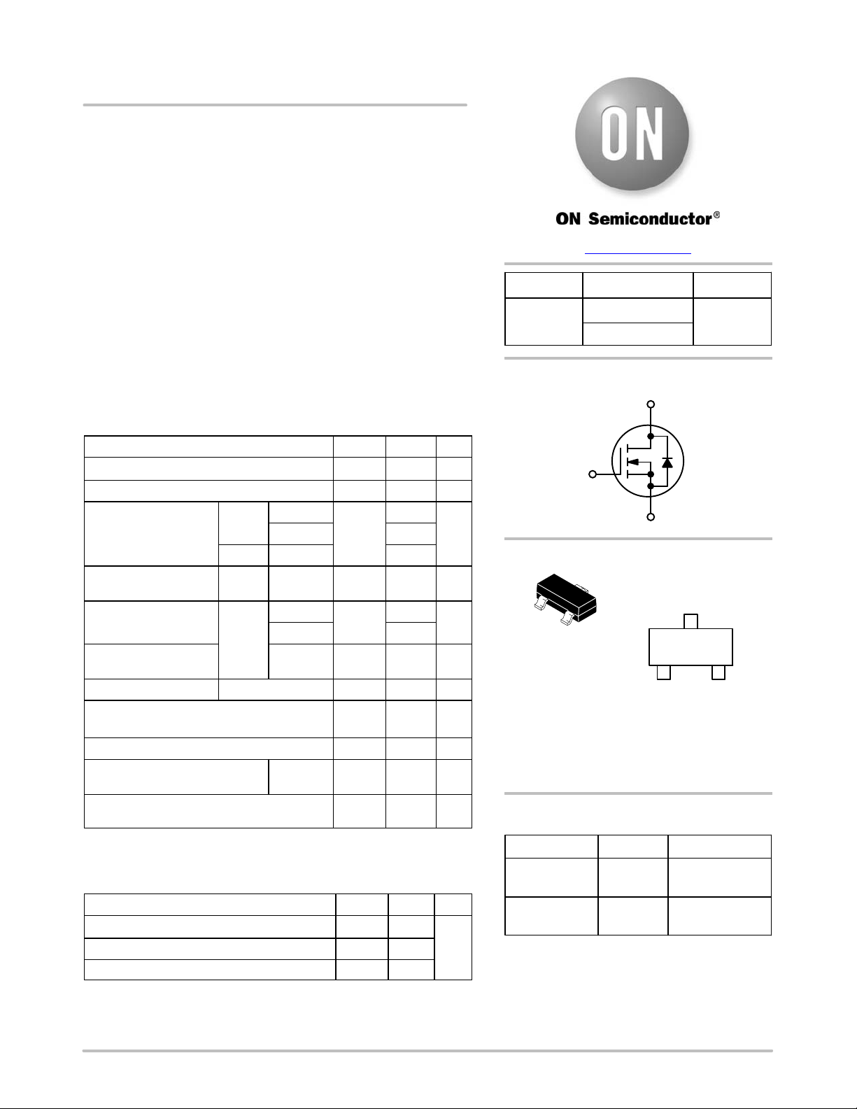
N−Channel
D
G
S
MARKING DIAGRAM/
3
1
2
SOT−23
CASE 318
STYLE 21
TR3 = Specific Device Code
M = Date Code
G = Pb−Free Package
(Note: Microdot may be in either location)
PIN ASSIGNMENT
3
Drain
TR3 MG
G
1
Gate2Source
ORDERING INFORMATION
Device Package Shipping
NTR4503NT1G SOT−23
(Pb−Free)
NVTR4503NT1G SOT−23
(Pb−Free)
†For information on tape and reel specifications,
including part orientation and tape sizes, please
refer to our Tape and Reel Packaging Specification
Brochure, BRD8011/D.
3000 / Tape & Ree
3000 / Tape & Ree
†
© Semiconductor Components Industries, LLC, 2015
May, 2015 − Rev. 7
1 Publication Order Number:
NTR4503N/D
Page 2
NTR4503N, NVTR4503N
ELECTRICAL CHARACTERISTICS (T
= 25°C unless otherwise noted)
J
Parameter Symbol Test Conditions Min Typ Max Units
OFF CHARACTERISTICS
Drain−to−Source Breakdown Voltage
Zero Gate Voltage Drain Current I
Gate−to−Source Leakage Current I
V
(BR)DSS
DSS
GSS
V
GS
V
GS
V
GS
= 0 V, V
V
DS
= 0 V, V
= 0 V, I
= 0 V, V
= 250 mA
D
DS
= 24 V, TJ = 125°C 10
DS
= "20 V "100 nA
GS
ON CHARACTERISTICS (Note 3)
Gate Threshold Voltage V
Drain−to−Source On−Resistance R
Forward Transconductance g
GS(TH)
DS(on)
FS
V
V
V
V
GS
GS
GS
DS
= VDS, I
= 10 V, I
= 4.5 V, I
= 4.5 V, I
= 250 mA
D
= 2.5 A 85 110 mW
D
= 2.0 A 105 140
D
= 2.5 A 5.3 S
D
CHARGES AND CAPACITANCES
Input Capacitance
Output Capacitance C
Reverse Transfer Capacitance C
Input Capacitance C
Output Capacitance C
Reverse Transfer Capacitance C
Total Gate Charge Q
Threshold Gate Charge Q
Gate−to−Source Charge Q
Gate−to−Drain Charge Q
Total Gate Charge Q
Threshold Gate Charge Q
Gate−to−Source Charge Q
Gate−to−Drain Charge Q
C
iss
oss
rss
iss
oss
rss
G(TOT)
G(TH)
GS
GD
G(TOT)
G(TH)
GS
GD
V
= 0 V, f = 1.0 MHz,
GS
V
GS
V
GS
V
GS
V
= 15 V
DS
= 0 V, f = 1.0 MHz,
V
= 24 V
DS
= 10 V, V
I
= 2.5 A
D
= 4.5 V, V
I
= 2.5 A
D
DS
DS
SWITCHING CHARACTERISTICS (Note 4)
Turn−On Delay Time
Rise Time t
Turn−Off Delay Time t
Fall Time t
Turn−On Delay Time t
Rise Time t
Turn−Off Delay Time t
Fall Time t
t
d(on)
d(off)
d(on)
d(off)
r
f
r
f
V
GS
I
D
V
GS
= 2.5 A, R
I
D
= 10 V, V
= 1 A, R
= 10 V, V
DD
= 6 W
G
DD
= 2.5 W
G
DRAIN−SOURCE DIODE CHARACTERISTICS
Forward Diode Voltage
Reverse Recovery Time t
Reverse Recovery Charge Q
V
SD
RR
RR
V
GS
V
= 0 V, I
GS
dIS/dt = 100 A/ms
= 0 V, I
= 2.0 A 0.85 1.2 V
S
= 2.0 A,
S
3. Pulse Test: Pulse Width v 300 ms, Duty Cycle v 2%.
4. Switching characteristics are independent of operating junction temperatures.
30 36 V
= 24 V 1.0 mA
1.0 1.75 3.0 V
135
pF
52
15
130 250
pF
42 75
13 25
nC
= 15 V,
3.6 7.0
0.3
0.6
0.7
nC
= 24 V,
1.9
0.3
0.6
0.9
ns
= 15 V,
5.8 12
5.8 10
14 25
1.6 5.0
ns
= 24 V,
4.8
6.7
13.6
1.8
9.2 ns
4.0 nC
www.onsemi.com
2
Page 3

NTR4503N, NVTR4503N
10
6
6
0
TYPICAL PERFORMANCE CURVES
10 V
6 V
5 V
8
4.5 V
4.2 V
6
4
DRAIN CURRENT (AMPS)
2
D,
I
0
0
V
1
, DRAIN−TO−SOURCE VOLTAGE (VOL TS)
DS
Figure 1. On−Region Characteristics
0.3
0.25
0.2
0.15
0.1
4 V
TJ = 25°C
3.8 V
3.6 V
3.4 V
3.2 V
3 V
2.8 V
2.6 V
ID = 2.5 A
= 25°C
T
J
VDS ≥ 10 V
8
4
100°C
25°C
DRAIN CURRENT (AMPS)
D,
I
432
2
0
TJ = −55°C
3
45
VGS, GATE−TO−SOURCE VOLTAGE (VOLTS)
Figure 2. Transfer Characteristics
0.12
TJ = 25°C
0.11
VGS = 4.5 V
0.10
0.09
0.05
DRAIN−TO−SOURCE RESISTANCE (W)
0
DS(on),
R
310
2
VGS, GATE−TO−SOURCE VOLTAGE (VOLTS)
57
46
Figure 3. On−Resistance vs. Gate−to−Source
Voltage
1.8
ID = 2.5 A
= 10 V
V
GS
1.6
1.4
1.2
DRAIN−TO−SOURCE
1.0
DS(on),
0.8
R
RESISTANCE (NORMALIZED)
0.6
−50 0−25 25
75 150
50 125100
TJ, JUNCTION TEMPERATURE (°C)
Figure 5. On−Resistance Variation with
Temperature
89
0.08
DRAIN−TO−SOURCE RESISTANCE (W)
VGS = 10 V
0.07
DS(on),
2
R
35
4
ID, DRAIN CURRENT (AMPS)
Figure 4. On−Resistance vs. Drain Current and
Gate Voltage
1000
VGS = 0 V
TJ = 150°C
100
, LEAKAGE (nA)
10
DSS
I
TJ = 100°C
1
53
10
15
20
25
VDS, DRAIN−TO−SOURCE VOLTAGE (VOL TS)
Figure 6. Drain−to−Source Leakage Current
vs. Voltage
www.onsemi.com
3
Page 4

NTR4503N, NVTR4503N
TYPICAL PERFORMANCE CURVES
300
VDS = 0 V
C
iss
VGS = 0 V
TJ = 25°C
200
C
rss
100
C, CAPACITANCE (pF)
C
oss
0
50
VGSV
DS
510 10
15
20 25
30
GATE−TO−SOURCE OR DRAIN−TO−SOURCE VOLTAGE (VOLTS)
Figure 7. Capacitance Variation
100
VDD = 24 V
= 2.5 A
I
D
V
= 10 V
GS
t
d(off)
t
f
10
t, TIME (ns)
t
d(on)
t
r
15
V
DS
Q
10
5
Q
GS
GATE−TO−SOURCE VOLTAGE (VOLTS)
0
GS,
021
V
Q
GD
G
QG, TOTAL GATE CHARGE (nC)
Figure 8. Gate−to−Source and
Drain−to−Source Voltage vs. Total Charge
3
VGS = 0 V
= 25°C
T
J
2
1
V
GS
ID = 2.5 A
T
J
3
= 25°C
15
10
5
DRAIN−TO−SOURCE VOLTAGE (VOLTS)
0
4
DS,
V
1
101
, GATE RESISTANCE (OHMS)
R
G
Figure 9. Resistive Switching Time Variation
vs. Gate Resistance
100
, SOURCE CURRENT (AMPS)
S
I
0
0.3
0.4
V
, SOURCE−TO−DRAIN VOLTAGE (VOLTS)
SD
0.6
0.7
Figure 10. Diode Forward Voltage vs. Current
0.9
10.5 0.8
www.onsemi.com
4
Page 5

NTR4503N, NVTR4503N
P
al
PACKAGE DIMENSIONS
SOT−23 (TO−236)
CASE 318−08
ISSUE AP
NOTES:
1. DIMENSIONING AND TOLERANCING PER ANSI Y14.5M, 1982.
D
H
SEE VIEW C
E
c
0.25
3
E
12
b
e
q
A
L
A1
L1
VIEW C
2. CONTROLLING DIMENSION: INCH.
3. MAXIMUM LEAD THICKNESS INCLUDES LEAD FINISH
THICKNESS. MINIMUM LEAD THICKNESS IS THE MINIMUM
THICKNESS OF BASE MATERIAL.
4. DIMENSIONS D AND E DO NOT INCLUDE MOLD FLASH,
PROTRUSIONS, OR GATE BURRS.
DIMAMIN NOM MAX MIN
A1 0.01 0.06 0.10 0.001
b 0.37 0.44 0.50 0.015
c 0.09 0.13 0.18 0.003
D 2.80 2.90 3.04 0.110
E 1.20 1.30 1.40 0.047
e 1.78 1.90 2.04 0.070
L 0.10 0.20 0.30 0.004
L1
H
E
q
STYLE 21:
PIN 1. GATE
MILLIMETERS
0.89 1.00 1.11 0.035
0.35 0.54 0.69 0.014 0.021 0.029
2.10 2.40 2.64 0.083 0.094 0.104
0 −−− 10 0 −−− 10
2. SOURCE
3. DRAIN
INCHES
NOM MAX
0.040 0.044
0.002 0.004
0.018 0.020
0.005 0.007
0.114 0.120
0.051 0.055
0.075 0.081
0.008 0.012
°°°°
SOLDERING FOOTPRINT*
0.95
SCALE 10:1
0.037
2.0
0.079
mm
ǒ
inches
Ǔ
0.95
0.037
0.9
0.035
0.8
0.031
*For additional information on our Pb−Free strategy and soldering
details, please download the ON Semiconductor Soldering and
Mounting Techniques Reference Manual, SOLDERRM/D.
ON Semiconductor and are registered trademarks of Semiconductor Components Industries, LLC (SCILLC). SCILLC owns the rights to a number of patents, trademarks,
copyrights, trade secrets, and other intellectual property. A listing of SCILLC’s product/patent coverage may be accessed at www.onsemi.com/site/pdf/Patent−Marking.pdf. SCILLC
reserves the right to m ake c hanges w ithout f urt her n otice t o a ny p roducts h erein. SCILLC makes no warranty, r epresentat ion o r g uar antee r egarding t he s uit ability o f i t s products for any
particular purpose, nor does SCILLC assume any liability arising out of the application or use of any product or circuit, and specifically disclaims any and all liability, including without
limitation special, consequent ial o r i ncidental d amages. “ Typical” parameters which may b e p rovided i n S CILLC d ata s heets and/or specifications can a nd d o v ary i n d iff erent applications
and actual performance may vary over time. All operating parameters, including “Typicals” must be validated for each customer application by customer’s technical experts. SCILLC
does not convey any license under its patent rights nor the rights of others. SCILLC products are not designed, intended, or authorized for use as components in systems intended for
surgical implant into t he b ody, or other applications int ended t o s upport o r s ustain l ife, o r for any other application in w hich t he f ailure of the SCILLC product could c reate a situation where
personal injury or death may occur. S hould B uyer p urchase o r u se S CILLC p r oduct s for any such unintended or unauthorized application, Buyer shall indemnify and hold SCILLC and
its officers, e mployees, s ubsidiaries, a ffiliat es, a nd d istributor s h arm less a gainst a ll c laims, c osts, d amages, a nd e xpenses, and r easonable a ttorney f ees a rising o ut o f, d irectly o r i ndirectly,
any claim of personal injury or death associated with such unintended or unauthorized use, even if such claim a lleges t hat SCILLC was negligent regarding the design or manufacture
of the part. SCILLC is an Equal Opportunity/Affirmative Action Employer. This literature is subject to all applicable copyright laws and is not for resale in any manner.
UBLICATION ORDERING INFORMATION
LITERATURE FULFILLMENT:
Literature Distribution Center for ON Semiconductor
P.O. Box 5163, Denver, Colorado 80217 USA
Phone: 303−675−2175 or 800−344−3860 Toll Free USA/Canada
Fax: 303−675−2176 or 800−344−3867 Toll Free USA/Canada
Email: orderlit@onsemi.com
N. American Technical Support: 800−282−9855 Toll Free
USA/Canada
Europe, Middle East and Africa Technical Support:
Phone: 421 33 790 2910
Japan Customer Focus Center
Phone: 81−3−5817−1050
www.onsemi.com
ON Semiconductor Website: www.onsemi.com
Order Literature: http://www.onsemi.com/orderlit
For additional information, please contact your loc
Sales Representative
NTR4503N/D
5
Page 6

 Loading...