

Page 1

NTE7151
Integrated Circuit
I2C Bus Control NTSC 1–Chip Color TV IC
Description:
The NTE7151 is an integrated circuit in a 56–Lead DIP type package designed for use as a PIF, SIF,
video, chroma and deflection circuit for NTSC color TVs. This device also provides audio/video
switching and a text interface.
Features:
PIF Circuit
D PLL Type IF Demodulation (Bus Alignment)
D Adjustment Free AFT Without Tank Coil
Video Circuit
D Black Stretcher
D DC Restoration Circuit
D D.L. Aperture Compensate Circuit (Bus Control)
D Internal Filter Auto–Adjust Circuit (FSC Link Type)
Chroma Circuit
D Color Control Circuit (Bus Control)
D Tint Control Circuit (Bus Control)
D RF AGC Output (Delay Point: Bus Alignment)
D Dual Time Constant Fast AGC
D Uni–Color Circuit (Bus Control)
D 3.58MHz Trap Filter Circuit (Bus ON/OFF)
D Y Delay Line Circuit
D B.P.F. / T.O.F. Circuit (Bus Select)
D Included ACC/Killer Filter
SIF Circuit
D Inter Carrier SIF System
D External Sound Select Switch (Bus Select)
Text Circuit
D Linear RGB Input
D Cut Off/Drive Adjustment (Bus Adjustment)
Deflection Circuit
D Adjustment Free Countdown System
D Sync. Separation Output
D X–Ray Protect Circuit
D Auto–Slicer Type High Performance Sync. Separation Circuit
D Horizontal and Vertical Position Adjustment (Bus Adjustment)
D Attenuator Circuit (Bus Control)
D RGB Primary Color Output
D Vertical Amplitude Adjustment (Bus Adjustment)
D Vertical Ramp Output
D Dual Time Constant AFC Circuit
Page 2
Absolute Maximum Ratings: (TA = +25°C unless otherwise specified)
Power Supply Voltage, V
CC
Power Dissipation, PDmax 2.19W. . . . . . . . . . . . . . . . . . . . . . . . . . . . . . . . . . . . . . . . . . . . . . . . . . . . . . . . .
Derate Above 25°C 17.5mW/°C. . . . . . . . . . . . . . . . . . . . . . . . . . . . . . . . . . . . . . . . . . . . . . . . . . . .
Input Terminal Voltage, V
Input Signal Amplitude, e
in
. . . . . . . . . . . . . . . . . . . . . . . . . . . . . . . . . . . . . . . . . . . . . . . . . . . . . . . .
in
Operating Temperature Range, T
Storage Temperature Range, T
stg
opr
GND–0.3V to VCC+0.3V. . . . . . . . . . . . . . . . . . . . . . . . . . . . . . . . . . . . . . . .
–20° to +65°C. . . . . . . . . . . . . . . . . . . . . . . . . . . . . . . . . . . . . . . . .
–55° to +150°C. . . . . . . . . . . . . . . . . . . . . . . . . . . . . . . . . . . . . . . . . .
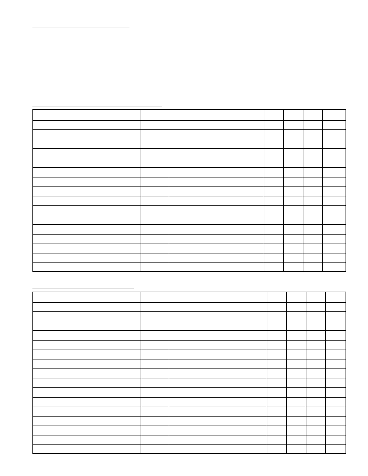
Recommended Operating Conditions:
Parameter Symbol Test Conditions Min Typ Max Unit
PIF Power Supply Voltage V
SIF Power Supply Voltage V
V/C/D Power Supply Voltage V
CCP
CCS
CCV
H. VCC Power Supply Voltage H. V
D. VCC Power Supply Voltage D. V
TV External Video Input Level V
Standard Video Input Level V
Standard Chroma Input Level V
FBP Width T
FBP Input Flow In Current I
in37/39
in43
in45
FBP
FBP
PIF Output Load Resistor R
SIF Output Load Resistor R
RGB Output Load Resistor R
Horizontal Output Load Resistor R
Vertical Output Load Resistor R
Sync.Separation Output Flow In Current I
ORGB
HOUT
VOUT
sync
CC
CC
Including Sync. – 1.0 – V
Including Sync. – 1.0 – V
At Burst Signal – 286 – mV
Vth = 1.4V, VCC = –1.4V 10 12 – µs
max – – 2 mA
OP
OS
maximum 10mA 330 800 – Ω
max – – 1 mA
8.5 9.0 9.5 V
8.5 9.0 9.5 V
8.5 9.0 9.5 V
8.5 9.0 9.5 V
2.7 3.3 3.8 V
2.0 8.2 – kΩ
1.0 8.2 – kΩ
– 1.8 – kΩ
4.1 5.7 – kΩ
4V
12V. . . . . . . . . . . . . . . . . . . . . . . . . . . . . . . . . . . . . . . . . . . . . . . . . . . . . . . . . .
P–P
P–P
P–P
P–P
DC Electrical Characteristics: (VCC = 9V, H. VCC = 9V, TA = +25°C unless otherwise specified)
Parameter Symbol Test Conditions Min Typ Max Unit
Sound Output (Pin1) V
Sound Output (Pin2) V
RF AGC (Pin3) V
AGC Filter (Pin5) V
1
2
3
5
PIF GND (Pin6) GND – 0.0 – V
PIF Input (Pin7) V
PIF Input (Pin8) V
PIF VCC (Pin9) V
Loop Filter (Pin10) V
APC Filter (Pin11) V
VCXO (Pin12) V
7
8
CC
10
11
12
V/C/D GND (Pin13) GND – 0.0 – V
F–BLK (Pin14) V
Analog R Input (Pin15) V
Analog G Input (Pin16) V
Analog B Input (Pin17) V
14
15
16
17
3.2 3.7 4.2 V
3.2 3.7 4.2 V
– 0.0 0.5 V
7.0 7.5 8.0 V
1.5 2.0 2.5 V
– 0.0 0.5 V
– 9.0 – V
– 4.5 – V
6.0 6.5 7.0 V
5.3 5.8 6.3 V
– 0.0 – V
4.4 4.9 5.4 V
4.4 4.9 5.4 V
4.4 4.9 5.4 V
Page 3
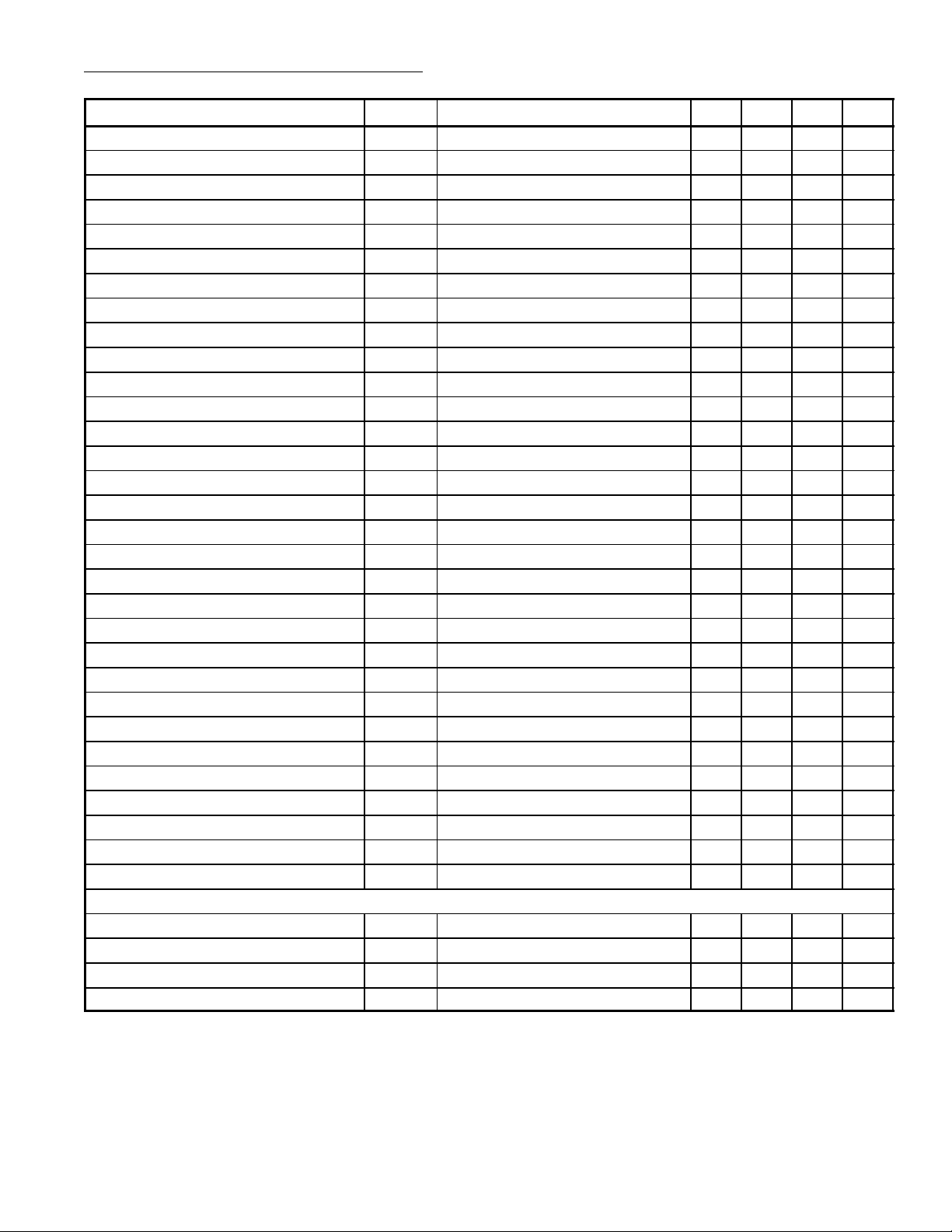
DC Electrical Characteristics (Cont’d): (VCC = 9V, H. VCC = 9V, TA = +25°C unless otherwise
specified)
Parameter Symbol Test Conditions Min Typ Max Unit
D. VCC (Pin18) V
R Output (Pin19) V
G Output (Pin20) V
B Output (Pin21) V
V SEPA (Pin25) V
H. VCC (Pin26) V
SCL (Pin27) V
SDA (Pin28) V
X–RAY (Pin29) V
H. AFC (Pin33) V
32fH VCO (Pin34) V
CC
BRT, C.O Cent 2.4 2.7 2.9 V
19
BRT, C.O Cent 2.4 2.7 2.9 V
20
BRT, C.O Cent 2.4 2.7 2.9 V
21
25
26
27
28
29
33
34
D. GND (Pin35) GND – 0.0 – V
ABL (Pin36) V
TV Input (Pin37) V
ACL (Pin38) V
EXT. Video Input (Pin39) V
Black DET (Pin40) V
AV/SW Output (Pin41) V
DC Rest (Pin42) V
Y Input (Pin43) V
AFT (Pin44) V
Chroma Input (PIn45) V
V / C / D VCC (Pin46) V
TV DET. Output (Pin47) V
SIF VCC (Pin48) V
BRT, COL Cent 2.9 3.4 3.9 V
36
37
BRT, COL Cent 2.9 3.4 3.9 V
38
39
40
41
42
43
44
45
46
47
CC
SIF GND (Pin51) GND – 0.0 – V
Limiter Input (Pin52) V
Audio TV Input (Pin53) V
De–Emphasis (Pin54) V
EXT. Audio Input (Pin55) V
EXT. Audio Input (Pin56) V
52
53
Pin4 GND 4.0 4.5 5.0 V
54
55
55
Current Consumption
IF Power Supply Current I
V / C / D Power Supply Current I
H. VCC Power Supply Current I
D. VCC Power Supply Current I
cci
ccv
cch
ccd
– 3.3 – V
5.8 6.3 6.8 V
– 9.0 – V
4.5 5.0 5.5 V
4.5 5.0 5.5 V
– 0.0 – V
7.0 7.5 8.0 V
5.5 6.0 6.5 V
2.9 3.0 3.9 V
1.1 1.6 2.1 V
6.1 6.6 7.1 V
1.8 2.3 2.8 V
5.5 6.0 6.5 V
4.0 4.5 5.0 V
2.0 2.5 3.0 V
1.6 1.85 2.1 V
– 9.0 – V
4.7 5.2 5.7 V
– 9.0 – V
– 0.0 0.5 V
2.5 3.0 3.5 V
2.5 3.0 3.5 V
2.5 3.0 3.5 V
32.8 46.0 52.0 mA
52.7 71.0 76.8 mA
10.7 14.0 18.4 mA
5.2 10.0 11.6 mA
Page 4

AC Electrical Characteristics: (VCC = 9V, H. VCC = 9V, TA = +25°C unless otherwise specified)
Parameter Symbol Test Conditions Min Typ Max Unit
PIF
Video Detected Output Level V
O1
V
O2
Input Sensitivity VINmin – 42 – dBµV
VINmax 100 107 – dBµV
Sync Tip Level V
Output Level for No Input V
SYNC
IF
Differential Gain DG – 2 5 %
Differential Phase DP – 2 5 DEG
PIF Output Frequency Characteristics f
c
Carrier Wave Compression Ratio CR 50 55 – dB
2nd Harmonics Compression Ratio HR 50 55 – dB
PIF Input Resistance R
PIF Input Capacitance C
iPIF
iPIF
Signal to Noise Ratio S/N 52 55 – dB
920kHz Beat I
IF AGC Range RW
IF AGC Voltage V
9200
AGC
5MEAN
V5max 7.4 7.6 – V
V5min – 3.8 – V
RF AGC Voltage V3max 7.7 8.2 – V
V3min – 0.0 0.5 V
RF AGC Control Range DG
AFT Center Voltage V
RFAGC
4CENT
AFT Voltage V4max 4.4 4.8 – V
V4min – 0.2 0.5 V
AFT Sensitivity m
AFT Output Resistance R
PIF VCO Control Sensitivity b
PIF VCO Pull–In Range f
PIF VCO Control Range ∆f
AFT
AFTOUT
IFVCO
ph
f
pl
PIFVCO
SIF
Sound Output Level V
Sound Distortion V
AAC
V
ADC
AUDIO
AMR AMR 50 60 – dB
Limiting Sensitivity V
Sound Output Frequency Characteristics f
Sound Output Resistance R
LIM
AUDIOH
f
AUDIOL
SOUT
1.7 2.0 2.3 V
2.0 2.5 3.0 V
P–P
P–P
2.6 2.9 3.2 V
4.8 5.2 5.6 V
5 7 – MHz
– 1.5 – kΩ
– 3.8 – pF
42 45 – dB
61 65 69 dB
4.2 4.5 4.8 V
35 40 – dB
2.2 2.5 2.8 V
– 40 – kHz/V
40 50 60 kΩ
2.0 2.5 – MHz/V
1.0 1.5 – MHz
1.0 1.5 – MHz
– 4.4 – MHz
400 500 600 mV
rms
– 4.5 – V
– 0.3 1.0 %
– 35 – dBµV
– 130 – kHz
– –130 – kHz
24 30 36 kΩ
Page 5

AC Electrical Characteristics (Cont’d): (VCC = 9V, H. VCC = 9V, TA = +25°C unless otherwise
specified)
Parameter Symbol Test Conditions Min Typ Max Unit
ATT
ATT Gain G
DC Voltage Drift V
Input Impedance R
Balance Characteristics B
ATTMAXE
G
ATTMAXT
G
ATTMEAN
G
ATTMIN
1VAR
V
1DC
i53
R
i55
MAX
B
MIN
Video
Input Impedance R
Input Dynamic Range V
Video Total Gain G
Video Frequyency Characteristic f
Maximum Output V
Black Expansion Amp Gain G
Black Expansion Start Point G
DC Restoration T
Sharpness Control Characteristics G
Sharpness Delay Time t
Contrast Control Characteristics G
H. V–BLK Output Voltage V
V–BLK Width T
fsc Trap Gain G
BAMP
BSTP
SHcent
G
SHmax
G
SHmin
SHDLY
CNcent
G
CNmin
VBLK
TRAP
i41
di41
Y
Y
do1
DC
BLK
OSD
OSD Switching Voltage V
OSD Delay Time t
OSD Delay Time Difference t
thOSD
OSDDLY
OSDD
OSD Rising Time tR – 15 30 ns
OSD Falling Time tF – 15 30 ns
Input Clamp Voltage V
OSD Gain G
Input Dynamic Range V
OSDC
OSD
diOSD
Cutoff Drive
Brightness Control Characteristics V
BRTmax
V
BRTcen
V
BRTmin
–2.0 0.0 +2.0 dB
4.0 6.0 8.0 dB
–16 –12 –9 dB
–99 –85 – dB
– – 50 mV
3.2 3.7 4.2 V
– 30 – kΩ
– 47 – kΩ
45 58 70 dB
–70 –58 –45 dB
100 – – kΩ
1.0 1.2 1.5 V
4.5 5.0 –
6.0 7.0 – MHz
7.5 8.0 – V
1.18 1.43 1.68
40 50 60 IRE
100 103 105 %
1 4 7 dB
9 12 15 dB
– –18 –15 dB
– 125 – ns
4.5 6.0 7.5 dB
22.5 24.0 28.5 dB
– 0.7 1.0 V
3.5 to 24.0 H
– –28 –20 dB
0.7 1.0 1.3 V
– 15 30 ns
– 5 10 ns
4.4 4.9 5.4 V
1.8 2.0 2.2
2.0 2.2 2.4 V
3.6 4.0 4.3 V
2.4 2.7 3.0 V
1.0 1.4 1.7 V
Page 6

AC Electrical Characteristics (Cont’d): (VCC = 9V, H. VCC = 9V, TA = +25°C unless otherwise
specified)
Parameter Symbol Test Conditions Min Typ Max Unit
Cutoff Drive (Cont’d)
Brightness Control Difference Between 3 Axes ∆
Cutoff Control Characteristics V
Drive Control Characteristics G
VRGB
cutmax
V
cutcen
V
cutmin
drvmax
G
drvmin
Chroma
Input Dynamic Range V
ACC Characteristics e
di45
e
a
b
A 0.9 1.0 1.1
Killer Point EK –48 –46 –43 dB
VCXO Frequency Control Range Df
VCXO Frequency Control Sensitivity b
VCXO Pull–In Range f
VCXO
VCXO
VCXOPL
Demodulate Relative Gain R/B 0.78 0.83 0.88
G/B 0.31 0.35 0.39
Demodulate Relative Phase R–B 84 91 98 DEG
G–B 233 240 247 DEG
Carrier Wave Remain E
Color Control Characteristics V
Uni–Color Control Characteristics G
Tint Control Characteristics q
Video Chroma Delay Time t
E
E
CG
CLRmax
G
CLRcen
G
CLRmin
UNIcen
G
UNImin
TNT cen
∆q
V–C
CR
CB
TNT
Deflection
Horizontal Free Running Frequency f
H. Out Pulse Duty T
H. Out Voltage V
VCO OSC Start Voltage V
H. Out Start Voltage V
H. Frequency Control Range Df
H. Frequency Control Sensitivity b
H. Sync Pull–In Range Df
H. Pull–In Stop Period T
H
H
HL
V
HH
OSCmin
HST
H
H
HPUL
HSTP
–50 0 +50 mV
0.5 0.65 0.8 V
– 0.0 – V
–0.8 –0.65 –0.5 V
3.75 4.25 4.75 dB
–4.0 –3.5 –3.0 dB
0.95 1.5 1.7 V
–23 –20 –17 dB
3 6 9 dB
±500 ±600 – Hz
– 1.0 – Hz/mV
±300 ±450 – Hz
– 20 40 mV
– 20 40 mV
– 20 40 mV
3.9 4.1 4.3 V
P–P
4.5 6.0 7.5 dB
38 40 – dB
4.5 6.0 7.5 dB
22 24 26 dB
–7 0 +7 DEG
±35 ±45 ±55 DEG
–30 0 +30 ns
–100 0 +100 Hz
38 41 44 %
– 0.2 0.3 V
2.5 3.0 3.5 V
3.0 3.5 4.0 V
3.7 4.0 – V
±500 ±650 – Hz
– 500 – Hz/V
±450 ±500 – Hz
259 to 272 H
P–P
P–P
P–P
Page 7

AC Electrical Characteristics (Cont’d): (VCC = 9V, H. VCC = 9V, TA = +25°C unless otherwise
specified)
Parameter Symbol Test Conditions Min Typ Max Unit
Deflection (Cont’d)
AFC–2 Control Range T
Horizontal Position Adjustment T
PAFC2
X–Ray Protection Detection Voltage V
X–Ray Protection Hold V oltage V
X–Ray Protection Hold Current V
Vertical Free Running Frequency f
V. Sync Pull–In Range T
T
VEND
V. Out Pulse Width T
V. Ramp Amplitude Control V
V
H. Sync Separation Level R
Forced V. OSC (262.5H) f
AFC2
XDET
XHLD
XLD
V
VST
V
VL
VH
sepa
V60
16 17 – µs
– ±3 – µs
3.35 3.5 3.65 V
3.9 4.2 4.5 V
80 100 120 µA
– 295 – H
– 224 – H
– 295 – H
– 8 – H
2.2 2.4 – V
– 1.6 1.8 V
30 35 40 %
– 60 – Hz
Pin Connection Diagram
Sound Outptu
Sound Output
RF AGC
SIF Tank
AGC Filter
PIF GND
PIF Input
PIF V
CC
APC Filter
VCXO
GND
F–BLK
Analog G Input
D. V
CC
R Output
V. Output
NFB
V. Ramp
V Sepa Filter
H. V
CC
SCL
SDA
1
2
3
4
5
6
7
8PIF Input
56
55
54
53
52 Limiter Input
51
50
49
9 48
47
11
46
44
15Analog R Input 42
16
17Analog B Input
18
19
20G Output
41 AV/SW Output
40 Black Det
39
38
37
35
23
34
27 30
28 29
Ext. Audio
Ext. Audio
De–Emphasis
Audio TV Input
SIF GND
PIF Tank
PIF Tank
SIF V
CC
TV Det. Output10Loop Filter
V
CC
Chroma Input12 45
AFT13
Y Input14 43
DC Restoration
Ext. Video
ACL
TV Input
ABL21B Output 36
D. GND22
32fH VCO
H. AFC24 33
H. Output25 32
Sync Output26 31
FBP Input
X–Ray
Page 8

56 29
128
2.000 (50.9) Max
.551 (14.0)
.165
(4.2)
.118 (3.0).070 (1.78)
.600 (15.24)
 Loading...