

Page 1

NTE7139
Integrated Circuit
Video Output Amplifier
Description:
The NTE7139 is a monolithic video output amplifier with a 6MHz bandwidth in a 9–Lead Staggered
SIP type medium power package. This device uses high–voltage DMOS technology and is intended
to drive the cathode of a CRT. To obtain maximum performance, the amplifier should be used with
black current control.
Features:
D No External Heatsink Required
D Black Current Measurement Output for Automatice Black Current Stabilization (ABS)
D Internal 2.5V Reference Circuit
D Internal Protection Against Positive Apperaing CRT Flashover Discharges
D Single Supply Voltage of 200V
D Simple Application with a Variety of Color Decoders
D Controlled Switch–Off Behaviour
Absolute Maximum Ratings: (Voltages referenced to GND (Pin4) unbless otherwise specified)
Supply Voltage, V
Inverting Input Voltage, V
Black Current Measurement Output Voltage, V
Cathode DC Output Voltage, V
Feedback Output Voltage, V
Low Non–Repetitive Peak Cathode Output Current, I
DD
in
om
. . . . . . . . . . . . . . . . . . . . . . . . . . . . . . . . . . . . . . . . . . . . . . . . . . . . .
ov
. . . . . . . . . . . . . . . . . . . . . . . . . . . . . . . . . . . . . . . . . . . . . . . . . . . . . . . .
of
oc(l)
(Flashover Discharge = 100µC, Note 2) 5A. . . . . . . . . . . . . . . . . . . . . . . . . . . . . . . . . . . . . . . . . .
High Non–Repetitive Peak Cathode Output Current, I
oc(h)
(Flashover Discharge = 100µC, Note 3) 10A. . . . . . . . . . . . . . . . . . . . . . . . . . . . . . . . . . . . . . . . .
Maximum Power Dissipation, P
Junction Temperatrure Range, T
Storage Temperature Range, T
Electrostatic Discharge, V
esd
max
J
stg
–20° to +150°C. . . . . . . . . . . . . . . . . . . . . . . . . . . . . . . . . . . . . . . . . .
–55° to +150°C. . . . . . . . . . . . . . . . . . . . . . . . . . . . . . . . . . . . . . . . . .
Note 4 ±2000V. . . . . . . . . . . . . . . . . . . . . . . . . . . . . . . . . . . . . . . . . . . . . . . . . . . . . . . . . . . . . . . . . . .
Note 5 ±300V. . . . . . . . . . . . . . . . . . . . . . . . . . . . . . . . . . . . . . . . . . . . . . . . . . . . . . . . . . . . . . . . . . . .
Thermal Resistance, Junction–to–Ambient (In Free Air, Note 6), R
Thermal Resistance, Junction–to–Case (Note 6), R
thJC
thJA
Note 1. Inputs and output are protected against electrostatic discharge in normal handling. However ,
to be total ly s afe, i t i s d esirabl e t o t ake n ormal p r ecautions a ppropri ate t o h andling M OS d evi ces.
Note 2. The cathode output is protected against peak currents (caused by positive voltage peaks
during high–resistance flash) of 5mA maximum with a charge content of 100µC.
Note 3. The cathode output is also protected against peak currents (caused by positive voltage
peaks during low–resistance flash) of 10mA maximum with a charge content of 100µC.
Note 4. Human body model: equivalent to discharging a 100pF capacitor through a 1.5kΩ resistor.
Note 5. Machine model: equivalent to discharging a 200pF capacitor through a 0Ω resistor.
Note 6. External heatsink not required.
250V. . . . . . . . . . . . . . . . . . . . . . . . . . . . . . . . . . . . . . . . . . . . . . . . . . . . . . . . . . . . . . .
8V. . . . . . . . . . . . . . . . . . . . . . . . . . . . . . . . . . . . . . . . . . . . . . . . . . . . . . . . . . .
6V. . . . . . . . . . . . . . . . . . . . . . . . . . . . . . . . . . . . . . . .
V
DD
V
DD
tbf W. . . . . . . . . . . . . . . . . . . . . . . . . . . . . . . . . . . . . . . . . . . . . . . . . .
56K/W. . . . . . . . . . . . . . . . .
12K/W. . . . . . . . . . . . . . . . . . . . . . . . . . . . . .
Page 2
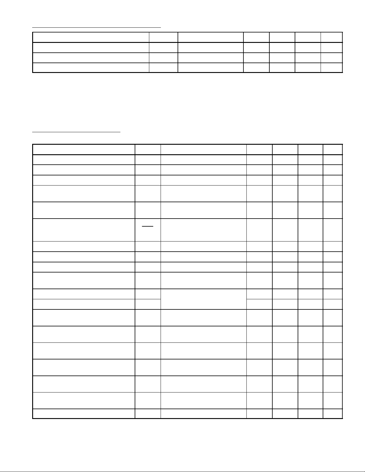
Recommended Operation Conditions:
Parameter Symbol Test Conditions Min Typ Max Unit
Supply Voltage V
Black Current Measurement Output Voltage V
Operating Ambient Temperature Range T
DD
om
Note 7 180 – 210 V
1.4 – 6.0 V
A
–20 – +65 °C
Note 7. The rating of supply voltage is 250V, but because of flash the maximum operating range for
supply voltage is 210V.
Electrical Characteristics: (VDD = 200V, Vom = 4V, TA = +25°C, CL = 10pF (CL consists of parasitic
and cathode capacitance) unless otherwise specified)
Parameter Symbol Test Conditions Min Typ Max Unit
Quiescent Voltage Supply Current I
Input Bias Current (Pin3) I
Internal Reference Voltage Input Stage V
Offset Current of Black Current
I
om(os)Ioc
Measurement Output
Temperature Drift of Internal
∆V
Reference Voltage Input Stage
DD
bias
V
V
V
int
Vom = 1.4 to 6 V
V
Tint
= 100V 2.8 3.0 3.3 mA
ocDC
= 100V 0 – 20 µA
ocDC
= 100V – 2.5 – V
ocDC
= 0µA, Vin = 1.5 to 3.5V,
= 100V – 0.5 – mV/K
ocDC
–10 – +10 µA
Linearity of Current Transfer ∆I
∆I
Maximum Peak Output Current (Pin9) I
Minimum Output Voltage (Pin8) V
Maximum Output Voltage (Pin8) V
Gain Bandwidth Product of
Open–Loop Gain Vos/V
i, dm
of(max)Voc
oc(min)Vin
oc(max)Vin
GB f = 500kHz, V
Small Signal Bandwidth BW
Large Signal Bandwidth BW
Cathode Output Propagation Delay
t
Time 50% Input to 50% Output
Cathode Output Rise Time
10% Output to 90% Output
Cathode Output Fall Time
90% Output to 10% Output
Setting Time 50% Input to
(99% < Output < 101%)
Slew Rate Between 50 and 150V SR Vin = 2V
Cathode Output Voltage Overshoot O
Ioc = –10µA to 3mA,
om
Vin = 1.5 to 3.5V,
oc
Vom = 1.4 to 6V
= 20V to VDD–30V – 25 – mA
= 3.5V – 7 12 V
= 1.5V VDD–14 VDD–10 – V
ocDC
V
= 60V
ocAC
V
ocDC
(p–p
= 100V
Voc = 50 to 150V Square Wave,
f < 1MHz, t
rin
= t
Voc = 50 to 150V Square Wave,
f < 1MHz, t
= 40ns
fin
Voc = 150 to 10V Square Wave,
f < 1MHz, t
= 40ns
rin
Voc = 50 to 150V Square Wave,
f < 1MHz, t
f < 1MHz, t
= t
rin
) Square Wave,
(p–p
= t
rin
Voc = 50 to 150V Square Wave,
f < 1MHz, t
rin
= t
pd
t
t
S
L
r
t
f
s
V
0.9 1.0 1.1
= 100V – 0.52 – GHz
),
5.0 6.0 – MHz
4.7 5.7 – MHz
38 49 60 ns
= 40ns
fin
62 74 87 ns
62 74 87 ns
– – 350 ns
= 40ns
fin
– 1200 – V/µs
= 40ns
fin
– 1 – %
= 40ns
fin
Power Supply Rejection Ratio SRR f < 50kHz, Note 8 – 60 – dB
Note 8. PSSR: The ratio of the change in supply voltage to the change in input voltage when there
is no change in output voltage.
Page 3

.827 (21.0)
Pin Connection Diagram
(Front View)
Feedback Output Voltage
9
Cathode Output Voltage
8
76N.C.
V
5
Black Current Measurement Output
GND (Substrate)
4
Inverting Input Voltage
3
N.C.
2
N.C.
1
DD
.130 (3.3) Dia
19
Seating Plane
.134
(3.42)
.590 (15.0)
.100 (2.54)
.242 (6.1)
(5.8)
.169
(4.3)
.118 (3.0) Min
.140
(3.56)
.065 (1.68)
.228
.728
(18.5)
.100 (2.54)
.250
(6.35)
.886 (22.0)
 Loading...