

Page 1

NTE7131
Integrated Circuit
DC–Coupled Vertical Deflection Circuit
Description:
The NTE7131 is an integrated circuit in a 9–Lead SIP type package designed for use in 90° and 110°
color deflection systems for field frequencies of 50 to 120Hz. The circuit provides a DC driven vertical
deflection output circuit, operating as a highly efficient class G system.
Features:
D Few External Components
D Highly Efficient Fully DC–Coupled Vertical Output Bridge Circuit
D Vertical Flyback Switch
D Guard Circuit
D Protection Against:
Short–Circuit of the Output Pins (7 and 4)
Short–Circuit of the Output Pins to V
D Temperature (Thermal) Protection
D High EMC Immunity because of Common Mode Inputs
D A Guard Signal in Zoom Mode
P
Absolute Maximum Ratings:
DC Supply
Supply Voltage, V
P
Non–Operating 40V. . . . . . . . . . . . . . . . . . . . . . . . . . . . . . . . . . . . . . . . . . . . . . . . . . . . . . . . . . . . . .
Operating 25V. . . . . . . . . . . . . . . . . . . . . . . . . . . . . . . . . . . . . . . . . . . . . . . . . . . . . . . . . . . . . . . . . . .
Flyback Supply Voltage, V
FB
Vertical Circuit
Output Current (Peak–to–Peak Value, Note 1), I
Output Voltage (Pin7), V
O(A)
O(p–p)
Flyback Switch
Peak Output Current, I
M
Thermal Data
Virtual Junction Temperature, T
Operating Ambient Temperatrure Range, T
Storage Temperature Range, T
VJ
A
stg
Thermal Resistance, Virtual Junction–to–Ambient (In Free Air), R
Thermal Resistance, Virtual Junction–to–Case, R
Short–Circuiting Time (Note 2), t
sc
thVJC
Note 1. IO maximum determined by current protection.
Note 2. Up to VP = 18V.
thVJA
50V. . . . . . . . . . . . . . . . . . . . . . . . . . . . . . . . . . . . . . . . . . . . . . . . . . . . . . . . .
2A. . . . . . . . . . . . . . . . . . . . . . . . . . . . . . . . . . . .
52V. . . . . . . . . . . . . . . . . . . . . . . . . . . . . . . . . . . . . . . . . . . . . . . . . . . . . . . . .
±1.5A. . . . . . . . . . . . . . . . . . . . . . . . . . . . . . . . . . . . . . . . . . . . . . . . . . . . . . . . . . .
+150°C. . . . . . . . . . . . . . . . . . . . . . . . . . . . . . . . . . . . . . . . . . . . . . . . .
–25° to +75°C. . . . . . . . . . . . . . . . . . . . . . . . . . . . . . . . . .
–55° to +150°C. . . . . . . . . . . . . . . . . . . . . . . . . . . . . . . . . . . . . . . . . .
40K/W. . . . . . . . . . . . . . . . .
4K/W. . . . . . . . . . . . . . . . . . . . . . . . . . . . . . . . .
1 Hour. . . . . . . . . . . . . . . . . . . . . . . . . . . . . . . . . . . . . . . . . . . . . . . . .
Page 2
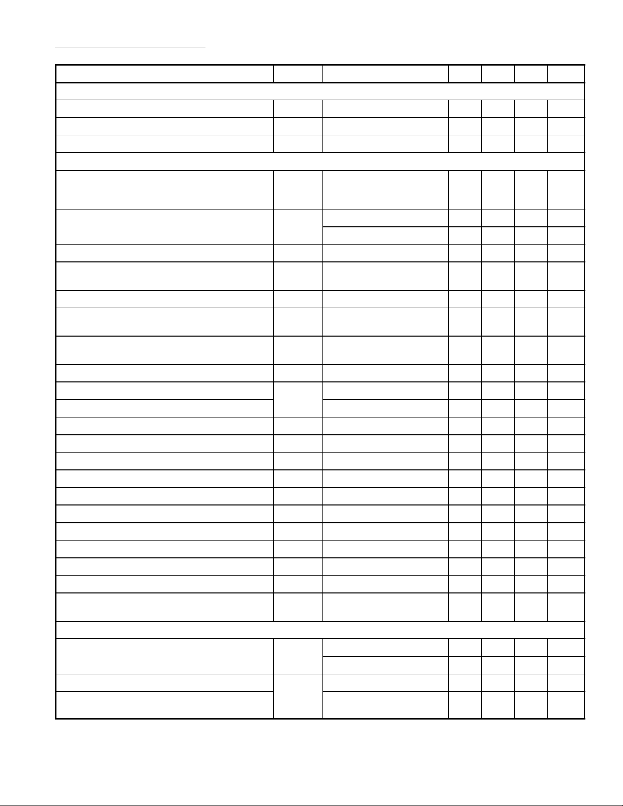
Electrical Characteristics: (VP = 14.5V, TA = +25°C, VFB = 45V, fi = 50Hz, I
otherwise specified)
Parameter Symbol Test Conditions Min Typ Max Unit
DC Supply
= 400µA unless
I(sb)
Operating Supply Voltage V
Flyback Supply Voltage V
Supply Current I
P
FB
No Signal, No Load – 30 55 mA
P
9.0 4.5 25.0 V
V
– 50 V
P
Vertical Circuit
Output Voltage Swing (Scan) V
Linearity Error LE IO = 2A
Output Voltage Swing (Flyback) V
Forward Voltage of the Internal Efficiency
Diode (V
O(A)
– VFB)
O(A)
– V
O(B)
V
V
Output Offset Current |IOS| I
Offset V oltage at the Input of the Feedback
Amplifier (V
I(fb)
– V
O(B)
)
Output Offset Voltage as a Function of
|VOS| I
∆VOST I
O
O
DF
I
= 0.6mA
diff
V
= 1.8V
diff
IO = 2A
(p–p)
(p–p)
IO = 50mA
I
= 0.3mA, IO = 1A (M) – 40 – V
diff
IO = –1A (M), I
= 0, I
diff
diff
diff
I(sb)
= 0, I
I(sb)
= 0 – – 72 µV/K
(p–p)
(p–p)
,
,
13.2 – – V
, Note 3 – 1 4 %
, Note 3 – 1 4 %
(p–p)
= 0.3mA – – 1.5 V
diff
= 50 to 500µA – – 40 mA
= 50 to 500µA – – 24 mV
Temperature
DC Output Voltage V
Open–Loop Voltage Gain (V
Open–Loop Voltage Gain (V
Voltage Ratio V
1–2/V9–4
7–4/V1–2
7–4/V9–4
) G
, V
= 0) Note 5 – 80 – dB
1–2
Frequency Response (–3dB) f
Current Gain (IO/I
) G
diff
O(A)Idiff
vo
V
R
res
I
= 0, Note 4 – 6.5 – V
Note 5, Note 6 – 80 – dB
– 0 – dB
Open Loop, Note 7 – 40 – Hz
– 5000 –
Current Gain Drift as a Function of Temperature ∆GcT – – 10
–4
K
Signal Bias Current I
Flyback Supply Current I
I(sb)
FB
During Scan – – 100 µA
50 400 500 µA
Power Supply Ripple Rejection PSRR Note 8 – 80 – dB
DC Input Voltage V
Common Mode Input Voltage V
Input Bias Current I
Common Mode Output Current I
I(DC)
I(CM)II(sb)
bias
O(CM)
I
I(sb)
∆I
fi = 50Hz, I
= 0 0 – 1.6 V
= 0 – 0.1 0.5 µA
I(sb)
= 300µA
diff
= 0
(p–p)
,
– 2.7 – V
– 0.2 – mA
Guard Circuit
Output Current I
Output Voltage on Pin8 V
O
O(guard)IO
Allowable Voltage on Pin8 Maximum Leakage
Not Active, V
Active, V
O(guard)
O(guard)
= 0V – – 50 µA
= 4.5V 1.0 – 2.5 mA
= 100µA – – 5.5 V
– – 40 V
Current = 10µA
Page 3

Notes:
Note 3. The linearity error is measured without S–correction and based on the same measurement
principle as performed on the screen. The measuring method is as follows:
Divide t he o utput s ignal I4 – I7 (VRM) i nto 2 2 e qual p arts r anging f rom 1 t o 2 2 i ncl usive. M easure
the value of two succeeding parts called one block starting with part 2 and 3 (block 1) and
ending w ith p ar t 2 0 a nd 2 2 ( block 1 0). T hus p art 1 and 2 2 a r e unused. The e quation f or l inear ity
error for adjacent blocks (LEAB) and not adjacent blocks (NAB) are given below
LEAD =
ak – a
a
(k + 1)
avg
; NAB =
a
max
– a
a
min
avg
Note 4. Related to VP.
Niote 5. V values within formulae, relate to voltages at or between relative pin numbers, i.e. V
7–4/V1–2
= voltage value across pins 7 and 4 divided by voltage value across pins 1 and 2.
Note 6. V
Note 7. Frequency response V
Note 8. At V
AC short–circuited.
9–4
= 500mV eff; measured across RM; fi = 50Hz.
(ripple)
7–4/V9–4
is equal to frequency response V
7–4/V1–2
.
Functional Description:
The vertical driver circuit is a bridge configuration. The deflection coil is connected between the output
amplifiers, which are driven in phase opposition. An external resistor (RM) connected in series with
the deflection coil provides internal feedback information. The differential input circuit is voltage driven. The input circuit has been adapted to enable it to be used with devices that deliver symmetrical
current signals. An external reisitor (R
) connected between the differential input determines the
CON
output current through the deflection coil. The relationship between the differential input current and
the output current is defined by: I
to 2A
mended that V
spread in the value of R
by varying RM. The maximum input differential voltage is 1.8V. In the application it is recom-
(p–p)
= 1.5V (Typ). This is recommended because of the spread of input current and the
diff
.
CON
diff
x R
CON
= I
x RM. The output current is adjustable from 0.5A
coil
(p–p)
The flyback voltage is determined by an additional supply voltage VFB. The principle of operating with
two supply voltages (class G) makes it possible to fix the supply voltage VP optimum for the scan voltage and the second supply voltage VFB optimum for the flyback voltage. Using this method, very high
efficiency is achieved.
The supply voltage VFB is almost totally available as flyback voltage across the coil, this being possible due to the absence of a decoupling capacitor (not necessary, due to the bridge configuration).
The output circuit is fully protected against the following:
D Thermal Protection
D Short–Circuit Protection of the Output Pins (Pin4 and Pin7)
D Short–Circuit of the Output pins to VP.
A guard circuit V
O(guard)
is provided. The guard circuit is activated at tghe following conditions:
D During Flyback
D During Short–Circuit of the Coil and During Short–Circuit of the Output Pins (Pin4 and Pin7) to
VP or GND
D During Open Loop
D When the Thermal Protection is Activated
This signal can be used for blanking the picture tube screen.
Page 4

Pin Connection Diagram
(Front View)
V
9
V
8
V
7
6
V
5
GND
4
V
3
V
I
2
drive (neg)
1
I
drive (pos)
I(fb)
O(guard)
O(A)
FB
O(B)
P
.961 (24.4)
.780 (19.8) .185 (4.7)
.489
(12.4)
.079
91
(2.0)
.674
(17.0)
.079 (2.0)
.100 (2.54)
 Loading...