

Page 1

NTE7109
Integrated Circuit
Switching Regulator Control
Description:
The NTE7109 is a primary switching regulator controller in a 16–Lead DIP type package designed
to get the regulated DC voltage from an AC power supply . This device can directly drive a MOSFET
with fast rise and fall output pulses.
The NTE7109 contains not only a high frequency OSC and fast output drive, but also a current limiter
with fast response and high sensibility so a true “fast switching regulator” can be realized. By adding
additional compenents to the primary side, a timer–type protection circuit can be made for protection
against short–circuit and overcurrent.
Features:
D 500kHz Operation to MOSFET
• Output Current: ±2A
• Output Rise Time: 60ns; Fall Time: 40ns
• Modified Totem–Pole Output Method with Low Through Current
D Compact and Light–Weight Power Supply
• Low Start–Up Current: 90µA Typ.
• Wide Range Between “Start–Up Voltage” and “Stop Voltage” make the Power Input Smooting
Capacitor Low; Start–Up Threshold Voltage: 16V; Stop Voltage: 10V
• High Power Dissipation Package withstands the Heat Generated bt the Gate–Drive Current
of a MOSFET
D Simplified Peripheral Circuit with Protection Circuit and Built–In Large–Capacity Totem–Pole
Output
• High–Speed Current Limiting Circuit using Pulse–by–Pulse Method (Two Systems of
CLM+pin, CLM–pin)
• Protection by Intermittent Operation of Output Overcurrent: Timer Protection Circuit
• Overvoltage Protection Circuit with an Externally Resettable Latch (OVP)
• Protection Circuit for Output Miss Action at Low Supply Voltage (UVLO)
D High–Performance and Highly Functional Power Supply
• Triangular Wave Oscillator for Easy Dead Time Setting
Applications:
D Feed Forward Regulator
D Flyback Regulator
Page 2
Absolute Maximum Ratings:
Supply Voltage, V
Collector Voltage, V
Output Current, I
CC
C
O
Peak ±2A. . . . . . . . . . . . . . . . . . . . . . . . . . . . . . . . . . . . . . . . . . . . . . . . . . . . . . . . . . . . . . . . . . . . . . .
Continuous ±0.5A. . . . . . . . . . . . . . . . . . . . . . . . . . . . . . . . . . . . . . . . . . . . . . . . . . . . . . . . . . . . . . . .
VF Terminal Voltage, V
ON/OFF Terminal Voltage, V
CLM – Terminal Voltage, V
CLM + Terminal Voltage, V
OVP Terminal Current, I
DET Terminal Voltage, V
DET Terminal Input Current, I
F/B Terminal Voltage, V
T–ON Terminal Input Current, I
. . . . . . . . . . . . . . . . . . . . . . . . . . . . . . . . . . . . . . . . . . . . . . . . . . . . . . . . . . . .
VF
ON/OFF
CLM –
CLM +
OVP
DET
DET
F/B
TON
T–OFF Terminal Input Current, I
Power Dissipation (T
= +25°C), P
A
Derate Above 25° 12mW/°C. . . . . . . . . . . . . . . . . . . . . . . . . . . . . . . . . . . . . . . . . . . . . . . . . . . . . . .
Junction Temperature, T
J
Operating Temperature Range, T
Storage Temperature Range, T
stg
. . . . . . . . . . . . . . . . . . . . . . . . . . . . . . . . . . . . . . . . . . . . . . . . . . .
TOFF
d
opr
–30° to +85°C. . . . . . . . . . . . . . . . . . . . . . . . . . . . . . . . . . . . . . . . .
–40° to +125°C. . . . . . . . . . . . . . . . . . . . . . . . . . . . . . . . . . . . . . . . . .
31V. . . . . . . . . . . . . . . . . . . . . . . . . . . . . . . . . . . . . . . . . . . . . . . . . . . . . . . . . . . . . . . .
31V. . . . . . . . . . . . . . . . . . . . . . . . . . . . . . . . . . . . . . . . . . . . . . . . . . . . . . . . . . . . . . .
V
CC
V
CC
–4.0 to +4.0V. . . . . . . . . . . . . . . . . . . . . . . . . . . . . . . . . . . . . . . . . . . . .
–0.3 to +4.0V. . . . . . . . . . . . . . . . . . . . . . . . . . . . . . . . . . . . . . . . . . . . .
8mA. . . . . . . . . . . . . . . . . . . . . . . . . . . . . . . . . . . . . . . . . . . . . . . . . . . . . . . .
6V. . . . . . . . . . . . . . . . . . . . . . . . . . . . . . . . . . . . . . . . . . . . . . . . . . . . . . . . . .
5mA. . . . . . . . . . . . . . . . . . . . . . . . . . . . . . . . . . . . . . . . . . . . . . . . . . . .
0 to 10V. . . . . . . . . . . . . . . . . . . . . . . . . . . . . . . . . . . . . . . . . . . . . . . . . . . . . . .
–1mA. . . . . . . . . . . . . . . . . . . . . . . . . . . . . . . . . . . . . . . . . . . . . . . . .
–2mA. . . . . . . . . . . . . . . . . . . . . . . . . . . . . . . . . . . . . . . . . . . . . . .
1.5W. . . . . . . . . . . . . . . . . . . . . . . . . . . . . . . . . . . . . . . . . . . . . . . . . .
+150°C. . . . . . . . . . . . . . . . . . . . . . . . . . . . . . . . . . . . . . . . . . . . . . . . . . . . . . . . .
Note 1. “+” sign shows the direction of current flow into the IC and “–” sigh shows the current flow
from the IC.
Note 2. This terminal has the constant voltage characteristic of 6V to 8V when current is supplied
from outside. The maximum allowable voltage is 6V when the constant voltage is applied
to this terminal. And maximum allowable current into this terminal is 5mA.
Note 3. The low impedance voltage supply should not be applied to the OVP terminal.
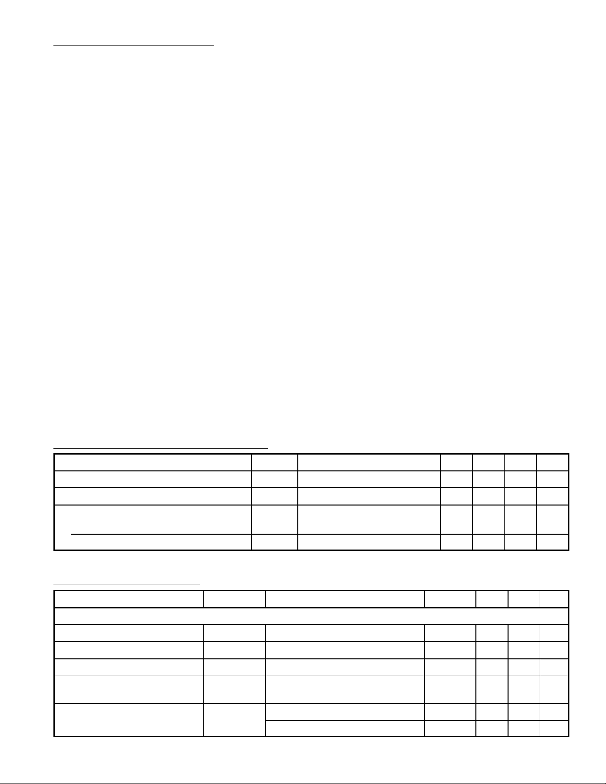
Recommended Operating Conditions:
Parameter Symbol Test Conditions Min Typ Max Unit
Supply Voltage Range V
Operating Frequency f
Oscillator Frequency Setting Resistance
T–ON Pin Resistance
T–OFF Pin Resistance R
OSC
R
OFF
CC
ON
12 18 30 V
– – 500 kHz
10 – 75 kΩ
2 – 30 kΩ
Electrical Characteristics: (VCC = 18V, TA = +25°C unless otherwise specified)
Parameter Symbol Test Conditions Min Typ Max Unit
Supply Voltage Circuit Current
Operating Supply Voltage Range V
Operation Start–Up Voltage V
Operation Stop Voltage V
Difference Between Operation
Start and Stop Voltage
Stand–By Current I
CC(STAR T)
CC(STOP)
∆V
CC
CCL
CC
V
CC(STOP)
15.2 16.2 17.2 V
9.0 9.9 10.9 V
∆VCC = V
VCC = 14.5V, TA = +25°C 50 90 140 µA
VCC = 14.5V, –30° ≤ TA ≤ +85°C 40 90 190 µA
CC(STAR T)
– V
CC(STOP)
5.0 6.3 7.6 V
– 30 V
Page 3

Electrical Characteristics (Cont’d): (VCC = 18V, TA = +25°C unless otherwise specified)
Parameter Symbol Test Conditions Min Typ Max Unit
Supply Voltage Circuit Current (Cont’d)
Operating Circuit Current I
Circuit Current in OFF State I
Circuit Current in Timer OFF State I
Circuit Current in OVP State I
CC OFF
CC CT
CC OVP
ON/OFF
High Threshold Voltage V
Low Threshold Voltage V
Hysterisis ∆V
THH ON/OFF
THL ON/OFF
TH ON/OFF
F/B
Current at 0% Duty I
Current at Maximum Duty I
FB MIND
FB MAXD
Current Difference Between Max
and 0% Duty
Terminal Voltage V
Terminal Resistance R
Detection
CCO
∆I
FB
FB
FB
VCC = 30V 10 15 21 mA
VCC = 25V 0.95 1.31 5.0 mA
VCC = 14V 50 90 140 µA
VCC = 25V 0.95 1.35 2.0 mA
VCC = 14V – 160 240 µA
VCC = 25V 1.3 2.0 3.0 mA
VCC = 14V 126 200 310
2.1 2.6 3.1 V
1.9 2.4 2.9 V
0.1 0.2 0.3 V
F/B Terminal Input Current –2.1 –1.54 –1.0 mA
F/B Terminal Input Current –0.90 –0.55 –0.40 mA
∆IFB = I
FB MIND
– I
FB MAXD
–1.35 –0.99 –0.70 mA
F/B Terminal Input Current = 0.95mA 4.9 5.9 7.1 V
420 600 780 Ω
Detection Voltage V
Input Current of Detection Amp I
Voltage Gain of Detection Amp G
OVP
High Threshol Voltage V
TH OVPH
Hysterisis Voltage ∆V
Threshold Current I
TH OVP
Input Current I
Reset Supply Voltage V
Difference Between Operation
Supply Voltage Stop and OVP
CC OVPC
V
CC (STOP)
–V
Reset
Current From OVP Terminal for
I
TH OVPC
OVP Reset
OVP
Threshold Voltage V
Input Current I
Reset Supply Voltage V
Difference Between Operation
Supply Voltage Stop and OVP
CC OVPC
V
CC (STOP)
–V
Reset
DET
IN DET
AV DET
TH OVP
IN OVP
CC OVPC
TH OVP
IN OVP
CC OVPC
2.4 2.5 2.6 V
V
= 2.5V – 1.0 3.0 µA
DET
30 40 – dB
540 750 960 mV
∆V
TH OVP
= V
TH OVPH
– V
TH OVPL
– 30 – mV
80 150 250 µA
V
= 400mV 80 150 250 µA
OVP
OVP Terminal is Open
(High Impedance)
7.5 9.0 10.0 V
0.55 1.20 – V
VCC = 30V –480 –320 –213 µA
VCC = 18V –210 –140 –93 µA
1.00 1.40 1.90 V
– 1.2 3.6 µA
7.6 8.6 9.6 V
0.65 1.30 – V
Page 4

Electrical Characteristics (Cont’d): (VCC = 18V, TA = +25°C unless otherwise specified)
Parameter Symbol Test Conditions Min Typ Max Unit
Timer
Timer Frequency I
Timer Charge Current I
TIM CH
OFF Time/ON Time Ratio TIME
CLM –
Threshold Voltage V
Input Current I
Delay Time from CLM– to V
OUT
TH CLM–
IN CLM–
T
PD CLM–
CLM +
Threshold Voltage V
Input Current I
Delay Time from CLM+ to V
OUT
TH CLM+
IN CLM+
T
PD CLM+
Oscillator
Oscillating Frequency f
Maximum ON Duty T
Upper Limit of Oscillation Waveform V
Lower Limit of Oscillation Waveform V
Difference Betwee Upper Limit and
∆V
Lower Limit Voltage of OSC
Waveform
TIMER
OFF/ON
OSC
DUTY
OSCH
OSCL
OSC
CT = 4.7µF 0.27 0.40 0.60 Hz
VCT = 3.3V, TA = –5°C –193 –138 –102 µA
TA = +25°C –178 –127 –94 µA
TA = +85°C –147 –105 –78 µA
7.0 8.7 11.0
–5° ≤ TA ≤ 85°C –220 –200 –180 mV
V
= –0.1V –170 –125 –90 µA
CLM–
– 170 – ns
–5° ≤ TA ≤ 85°C 180 200 220 mV
V
= –0.1V –270 –205 –140 µA
CLM+
– 130 – ns
RON = 20kΩ, R
OFF
= 17kΩ,
CF = 220pF, –5° ≤ TA ≤ 85°C
f
= 188kHz 3.97 4.37 4.77 V
OSC
f
= 188kHz 1.76 1.96 2.16 V
OSC
f
= 188kHz 2.11 2.41 2.71 V
OSC
170 188 207 kHz
47 50 53 %
V
F
OSC Frequency in CLM Operating
f
OSC VF
State
Duty in CLM Operating State T
Timer Operating Start Voltage V
VF DUTY
TH TIME
Input Current I
Output
Output Low Voltage V
V
V
V
Output High Voltage V
V
Output Voltage Rise Time T
Output Voltage Fall Time t
VF
OL 1
OL 2
OL 3
OL 4
OH 1
OH 2
RISE
FALL
VF = 5V
VF = 2V
RON = 20kΩ, R
CF = 220pF
OFF
= 17kΩ,
170 188 207 kHz
108 124 143 kHz
VF = 0.2V, Min OFF Duty/Max ON Duty 11.0 13.7 22.0
2.7 3.0 3.3 V
Source Current – 2 6 µA
VCC = 18V, IO = 10mA – 0.05 0.4 V
VCC = 18V, IO = 100mA – 0.7 1.4 V
VCC = 5V, IO = 1mA – 0.69 1.0 V
VCC = 5V, IO = 100mA – 1.3 2.0 V
VCC = 18V, IO = –10mA 16.0 16.5 – V
VCC = 18V, IO = –100mA 15.5 16.0 – V
No Load – 50 – ns
No Load – 35 – ns
Page 5

Pin Connection Diagram
Collector
V
OUT
Emitter
ON/OFF
OVP (Shut Down)
DET
V
F
F/B
1
2
3
4
5
6
7
8
16 9
V
16
CC
CLM (+)
15
CLM (–)
14
GND
13
CT
12
11
T – OFF
OSC Capacitance
10
T – ON
9
.245
(6.22)
Min
.260 (6.6) Max
18
.785 (19.9) Max
.300 (7.62)
.200 (5.08)
Max
.100 (2.54)
.700 (17.7)
 Loading...