

Page 1
NTE7047
Integrated Circuit
TV Color Small Signal Sub System
Features:
D Vision IF Amplifier with Synchronous Demodulator
D Automatic Gain Control (AGC) Detector Suitable for Negative Modulation
D AGC Tuner
D Automatic Frequency Control (AFC) Circuit with Sample–and–Hold
D Video Preamplifier
D Sound IF Amplifier and Demodulator
D DC Volume Control or Separate Supply for Starting the Horizontal Oscillator
D Audio Preamplifier
D Horizontal Synchronization Circuit with Two Control Loops
D Vertical Synchronization (Divider System) and Sawtooth Generation with Automatic Amplitude
Adjustment for 50Hz and 60Hz
D Transmitter Identification (Mute)
D Generation of Sandcastle Pulse
Absolute Maximum Ratings:
Supply Voltage (Pin7), VP = V
Total Power Dissipation, P
7–6
tot
Operating Ambient Temperature Range, T
Storage Temperature Range, T
stg
A
–25° to +65°C. . . . . . . . . . . . . . . . . . . . . . . . . . . . . . . . . . .
–25° to +150°C. . . . . . . . . . . . . . . . . . . . . . . . . . . . . . . . . . . . . . . . . .
13.2V. . . . . . . . . . . . . . . . . . . . . . . . . . . . . . . . . . . . . . . . . . . . . . . . . . .
2.3W. . . . . . . . . . . . . . . . . . . . . . . . . . . . . . . . . . . . . . . . . . . . . . . . . . . . . . . .
Electrical Characteristics: (TA = +25°C, VP = V
= 12V, carrier 38.9MHz, negative modulation
7–6
unless otherwise specified)
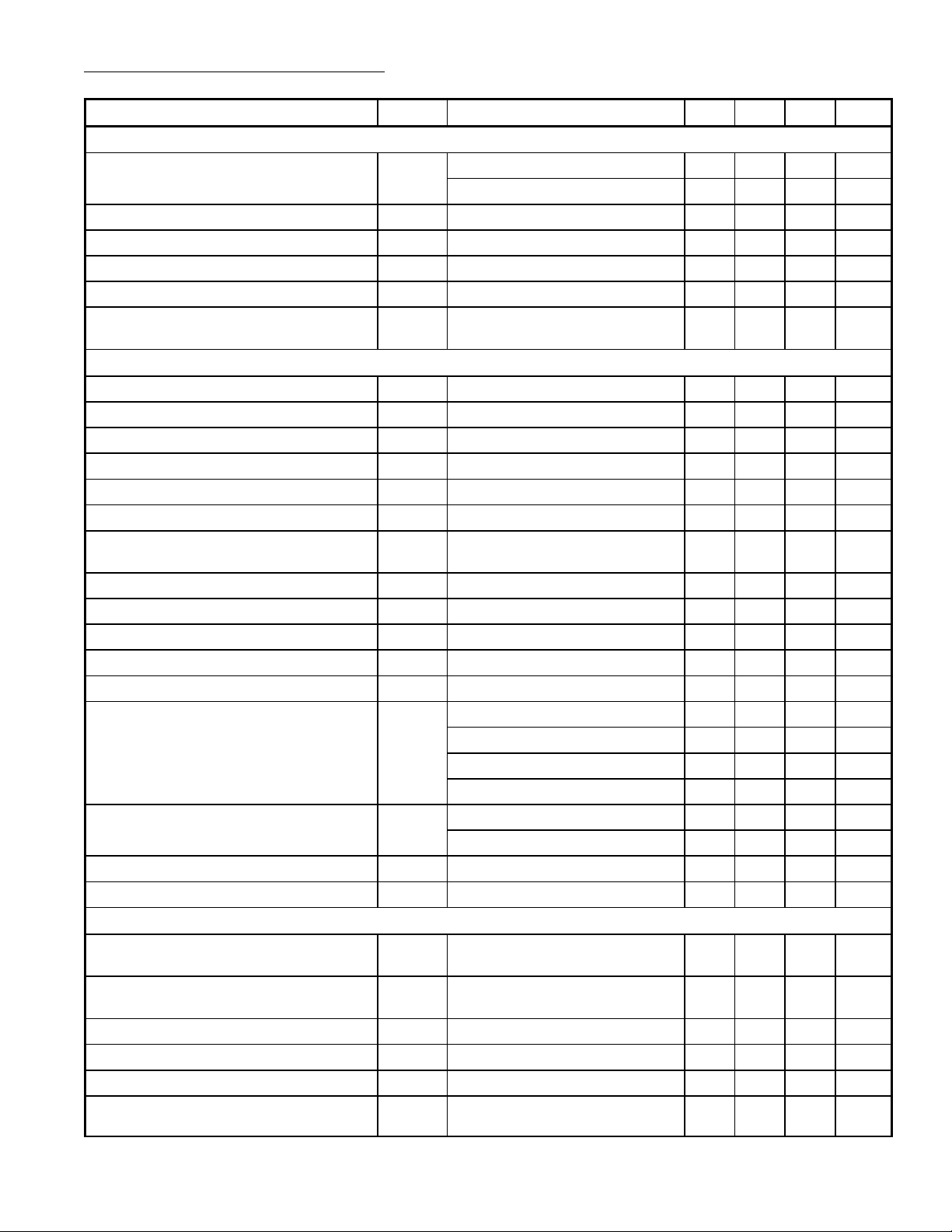
Parameter Symbol Test Conditions Min Typ Max Unit
Supplies
Supply Voltage Range (Pin7) V
Supply Current (Pin7) I
Start Current (Pin11) I
Start Voltage Horizontal Oscillator V
Start Protection Level V
7–6
7
11
11
11
At no input 75 125 165 mA
Note 1 – 6.5 9.0 mA
I11 = 12mA – – 16.5 V
9.5 12.0 13.2 V
9.5 – – V
Note 1. Pin11 has a double function. When during switch–on a current of 9mA is supplied to this pin,
it is used to start the horizontal oscillator. The main supply can then be obtained from the
horizontal deflection stage. When no current is supplied to this pin it can be used as a volume
control.
Page 2
Electrical Characteristics (Cont’d): (TA = +25°C, VP = V
modulation unless otherwise specified)
Parameter Symbol Test Conditions Min Typ Max Unit
Vision IF Amplifier (Pin8 and Pin9)
= 12V, carrier 38.9MHz, negative
7–6
Input Sensitivity (RMS Value) V
At 38.9MHz, Note 2 25 40 60 µV
8–9
At 45.75MHz, Note 2, Note 26 25 40 60 µV
Differential Input Resistance R
Differential Input Capacitance C
Gain Control Range G
Maximum Input Signal V
Output Signal Expansion for 48dB
∆V
Note 3 – 1300 – Ω
8–9
Note 3 – 5 – pF
8–9
8–9
8–9
Note 4 – 1 – dB
17
– 77 – dB
100 170 – mV
Variation of Input Signal
Video Amplifier (Note 5)
Zero Signal Output Level V
Top Sync Level V
Video Output Signal Amplitude V
Note 6 – 50.4 – V
17
17
Note 7 2.3 2.65 3.0 V
17
2.3 2.5 2.7 V
White–Spot Threshold Level – 5.7 – V
White–Spot Insertion Level – 3.8 – V
Video Output Impedance – 25 – Ω
Internal Bias Current of Output Transistor
I
17(int)
1.4 1.8 – mA
(NPN Emitter Follower)
Maximum Source Current I
17
10 – – mA
Bandwidth of Demodulated Output Signal B 5 7 – MHz
Differential Gain G
Note 8 – 4 8 %
17
Differential Phase j Note 8 – 2 5 deg.
Video Non–Linearity NL Note 9 – 2 5 %
Intermodulation f = 1.1MHz (Blue), Note 10 50 60 – dB
f = 1.1MHz (Yellow), Note 10 50 60 – dB
f = 3.3MHz (Blue), Note 10 55 65 – dB
f = 3.3MHz (Yellow), Note 10 55 65 – dB
Signal–to–Noise Ratio S/N Vi = 10mV, Note 11 50 57 – dB
End of gain control range, Note 11 50 62 – dB
Residual Carrier Signal V
Residual 2nd Harmonic of Carrier Signal V
17
17
– 2 10 mV
– 2 10 mV
Tuner AGC
Minimum Starting Point Tuner Take–Over
V
8–9(rms)
(RMS Value)
Maximum Starting Point Tuner Take–Over
V
8–9(rms)
(RMS Value)
Maximum Tuner AGC Output Swing I
5(max)V5
Output Saturation Voltage V
Leakage Current (Pin5) I
Input Signal Variation Complete Tuner
Control
5(sat)I5
L
∆V
i
– – 0.2 mV
100 150 – mV
= 3V 4 – – mA
= 2mA – – 300 mV
– – 1 µA
0.5 2.0 4.0 dB
Page 3
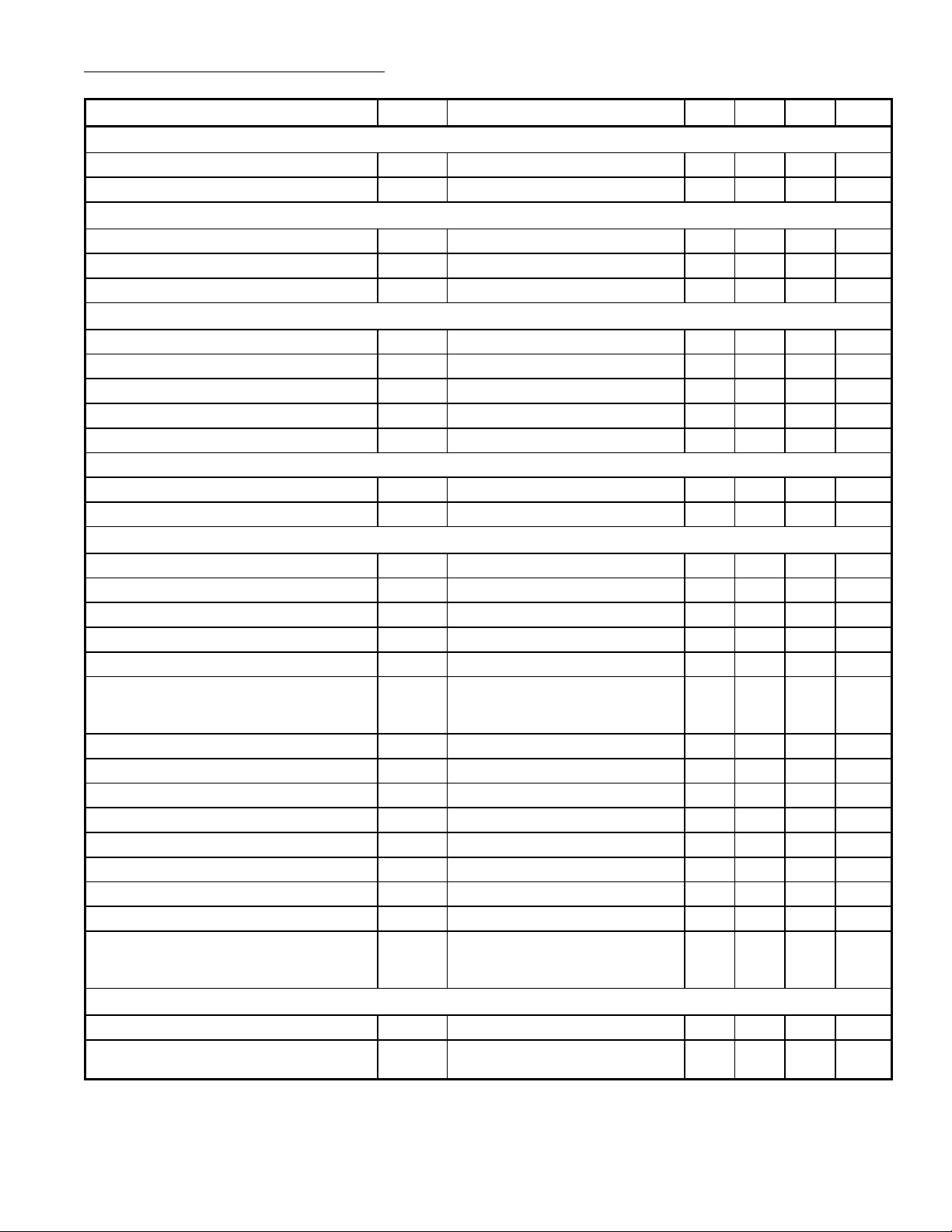
Electrical Characteristics (Cont’d): (TA = +25°C, VP = V
= 12V, carrier 38.9MHz, negative
7–6
modulation unless otherwise specified)
Parameter Symbol Test Conditions Min Typ Max Unit
Tuner AGC (Cont’d)
Minimum Voltage Tuner Take–Over V
Voltage to Switch on the X–Ray Protection V
1
Horizontal output high resistance – – 0.8 V
1
AFC Circuit (AFC Sample–and–Hold/Switch)
AFC Switch–Off Current I
Output Current I
Leakage Current at Pin19 I
19
19
LO
V19 = 0V – 0.1 0.3 mA
AFC Circuit (AFC Output)
AFC Output Voltage Swing V
Available Output Current I
Note 12, Note 13 10.5 – 11.5 V
18
18
Control Steepness – 100 – mV/kHz
AFC Output Voltage with AFC Off V
AFC Output Resistance R
18
18
Measured With an Input Signal Amplitude = 150µV (RMS value)
Output Voltage Swing V
Note 26 – 11 – V
18
Control Steepness Note 26 – 80 – mV/kHz
Sound Circuit (Note 14)
Input Limiting Voltage V
Input Resistance R
Input Capacitance C
15
15
15
V
o(max)
= –3dB – 400 800 µV
AM Suppression AMS 53 58 – dB
AF Output Signal (RMS Value) V
AF Output Signal when Pin11 is used as
12(rms)
V
12(rms)
Note 15 400 600 800 mV
∆f = 50kHz 500 900 1500 mV
a Starting Pin or Connected to
VP (RMS Value)
AF Output Impedance Z
12
Total Harmonic Distortion THD Note 16 – 0.5 2.0 %
Ripple Rejection RR Volume control 20dB; fk = 100Hz – 35 – dB
Output Voltage When Muted V
Output Level Shift due to Muting V
12
Volume control –20dB – – 0.5 V
12
Signal–to–Noise Ratio S/N Note 17 – 47 – dB
Voltage with Pin11 Disconnected V
Current with Pin11 Short Circuited to GND I
Temperature Dependence of the Output
Signal Amplitude
11
11
V
TA = +20° to +65°C,
12
–30dB volume control and
voltage of Pin11 fixed, Note 26
Volume Control (Note 18)
External Control Resistor R
Suppression Output Signal during
OSS 60 66 – dB
Note 18 – 4.7 – kΩ
11
Mute Condition
– – 1 V
0.1 – – mA
– – 2 µA
0.2 – – mA
5.5 6.0 6.5 V
– 40 – kΩ
– 2.6 – kΩ
– 6 – pF
– 25 100 Ω
– 2.5 – V
– 6.0 – V
– 1 – mA
– 2.5 – dB
Page 4

Electrical Characteristics (Cont’d): (TA = +25°C, VP = V
= 12V, carrier 38.9MHz, negative
7–6
modulation unless otherwise specified)
Parameter Symbol Test Conditions Min Typ Max Unit
Horizontal Synchronization Circuit (Sync Separator)
Required Sync Pulse Amplitude V
Input Current, Pin25 I
Horizontal Synchronization Circuit (First Control Loop)
Holding Range PLL ±∆f – 1500 2000 Hz
Catching Range PLL ±∆f 600 1500 – Hz
IF Input Signal at which the Time Constant
V
is Switched (RMS Value)
Horizontal Synchronization Circuit (Second Control Loop)
Control Sensitivity ∆td/∆toNote 21 – 100 –
Control Range t
Controlled Edge positive
Horizontal Synchronization Circuit (Phase Adjustment, via Second Control Loop)
Control Sensitivity – 25 – µA/µs
Maximum Allowed Phase Shift α – ±2 – µs
Horizontal Synchronization Circuit (Horizontal Oscillator, Pin23)
Free Running Frequency f
Spread with Fixed External Components ∆f – – 4 %
Frequency Variation ∆f
Frequency Variation with Temperature TC Note 26 – –1.6 – Hz/°C
Maximum Frequency Deviation at Start
∆f
of Horizontal Output
Frequency Variation when Only Noise
∆f
is Received
Horizontal Synchronization Circuit (Horizontal Output)
Output Limiting Voltage V
Output Voltage LOW V
Maximum Sink Current I
Duty Cycle Output Signal – 46 – %
Rise Time of Output Pulse t
Fall Time of Output pulse t
Horizontal Synchronization Circuit (Flyback Input and Sandcastle Output, Note 22)
Input Current Required During
I
Flyback Pulse
Output Voltage During Burst Key Pulse V
Output Voltage During Horizontal Blanking V
Output Voltage During Vertical Blanking V
Pulse Width, Burst Key Pulse t
Pulse Width, Horizontal Blanking Pulse Flyback Pulse Width
Note 19 200 750 – mV
25
V25 > 5V – 8 – µA
25
V25 = 0V – –10 – mA
Strong to weak – 2.2 – mV
8–9
d
R = 34.3kΩ, C = 2.7nF – 15625 – Hz
fr
∆VP = 9.5 to 13.2V – – 2 %
fr
fr
Note 26 – – 500 Hz
fr
26
I
26
26
r
f
27
27
27
27
W
= 10mA – 0.2 0.5 V
sink
60Hz 2.9 3.3 3.7 µs
– 25 – µs
– – 10 %
– – 16.5 V
10 – – mA
– 260 – ns
– 100 – ns
0.1 – 2.0 mA
8 – – V
4.0 4.4 5.0 V
2.1 2.5 2.9 V
50Hz 3.2 3.6 4.0 µs
Page 5

Electrical Characteristics (Cont’d): (TA = +25°C, VP = V
= 12V, carrier 38.9MHz, negative
7–6
modulation unless otherwise specified)
Parameter Symbol Test Conditions Min Typ Max Unit
Horizontal Synchronization Circuit (Cont’d) (Flyback Input and Sandcastle Output, Note 22)
Vertical Blanking Pulse 50Hz divider in search window – 21 – lines
60Hz divider in search window – 17 – lines
50Hz divider in narrow window – 25 – lines
60Hz divider in narrow window – 21 – lines
Delay Between Start of Sync Pulse at
the Video Output and the Burst Key
Pulse
Horizontal Synchronization Circuit (Coincidence Detector)
Voltage for Synchronized Condition V
Voltage for No Signal Condition V
Switching Level to Switch the Phase
V
Detector from Fast to Slow
Hysteresis Slow to Fast V
Switching Level to Activate the Mute
V
Function (Transmitter Identification)
Hysteresis Mute Function V
Delay Time of Mute Release after
Transmitter Insertion
Allowable Load on Pin22 – – 10 µA
External Video Mode V
Current at Pin22 I
Vertical Circuit (Vertical Ramp Generator, Note 24)
Input Current During Scan I
Discharge Current During Retrace I
Sawtooth Amplitude (peak–to–peak value) V
2(p–p)
Interlace Timing of the Internal Pulses 30 32 34 µs
Vertical Circuit (Vertical Output, Note 24)
Available Output Current I
Maximum Output Voltage V
Vertical Circuit (Vertical Feedback Input, Note 24)
Input Voltage, DC Component V
Input Voltage, AC Component
V
4(p–p)
(peak–to–peak value)
Input Current I
Internal Precorrection to Sawtooth ∆t
Deviation Amplitude 50Hz/60Hz – – 2 %
Temperature Dependence of the
Amplitude
Vertical Circuit (Vertical Guard, Note 24, Note 25)
Active Switching Level at a Deviation
∆V
with Respect to the DC Feedback
Level: Guard Level LOW
Trailing edge, 60Hz – – 9.3 µs
Rising edge 4.7 5.4 6.1 µs
22
22
22
22
22
22
– 9.8 – V
– 1.5 – V
6.2 6.7 7.2 V
– 0.6 – V
2.5 2.8 3.1 V
– 2 – V
– – 300 µs
22
V22 = 0V – – 0.8 mA
22
2
2
– – 0.7 V
– – 2 µA
– 0.8 – mA
– 1.9 – V
V3 = 4V – – 3 mA
3
I3 = 0.1mA 4.4 5.0 – V
3
4
2.9 3.3 3.7 V
– 1 – V
4
p
– – 12 µA
– 3 – %
TA = +20°C to +65°C – – 2 %
V27 = 2.5V – 2.1 – V
4
Page 6

Electrical Characteristics (Cont’d): (TA = +25°C, VP = V
= 12V, carrier 38.9MHz, negative
7–6
modulation unless otherwise specified)
Parameter Symbol Test Conditions Min Typ Max Unit
Vertical Circuit (Cont ’d) (Vertical Guard, Note 24, Note 25)
Active Switching Level at a Deviation
with Respect to the DC Feedback
Level: Guard Level HIGH
∆V
V27 = 2.5V – 2.0 – V
4
Notes:
Note 2. On set AGC.
Note 3. The input impedance has been chosen such that a SAW–filter can be applied.
Note 4. Measured with 0dB = 450µV.
Note 5. Measured at 10mV (RMS value) top sync input signal.
Note 6. So–called projected zero point; i.e. with switched demodulator.
Note 7. White 10% of the top sync amplitude.
Note 8. The differential gain is expressed as a percentage of the difference in peak amplitude be-
tween the largest and smallest value relative to the subcarrier amplitude at blanking level.
The differential phase is defined as the difference in degrees between the largest and smallest phase angle. The differential gain and phase are measured with a DSB signal.
Note 9. This figure is valid for the complete video signal amplitude (peak white–to–black). The non–
linearity is expressed as a percentage of the maximum deviation of a luminance step from
the mean step, with respect to the mean step.
Note10. The figures are measured at an input signal of 10mV (RMS value).
Note11. Measured with a source impedance of 75Ω.
V
Signal–to–noise ratio = 20 log
out black–to–white
V
at B = 5MHz
n(rms)
Note12. The AFC control voltage is obtained by multiplying the IF output signal (which is also used
to drive the synchronous demodulator) with a reference carrier. This reference carrier is ob-
tained from the demodulator tuned circuit via a 90 degree phase shift network. The IF output
signal has an asymmetrical frequency spectrum with respect to the carrier frequency. To
avoid problems due to this asymmeterical signal the AFC circuit is followed by a sample–
and–hold circuit which samples during the sync level. As a result the AFC output voltage con-
tains no video information. The specified control steepness is without using an external load
resistor. The control steepness decreases when the AFC output is loaded with two resistors
between the voltage supply and GND.
Note13. At very weak input signals the drive signal for the AFC circuit will have a high noise content.
This noise input has an asymmetrical frequency spectrum which will cause an offset of the
AFC output voltage. To avoid problems due to this effect a notch filter can be built in to the
demodulator tuned circuit. The characteristics given for waek input signals are measured
without a notch circuit, with a SAW filter connected in front of the IC (input signal such that
the input signal of the IC is 150µV (RMS value).
Note 14. The sound circuit is measured (unless otherwise specified) with an input signal of V15 of
50mV (RMS value), a carrier frequency of 5.5MHz at a ∆f of 27.5kHz and AF frequency of
1kHz. The QL of the demodulator tuned circuit is 16 and the volume control is connected to
the supply . The reference circuit must be tuned in such a way that the output is symmetrical
clipping at maximum volume.
Note15. The output signal is measured at a ∆f = 7.5kHz and maximum volume control.
Note16. The demodulator tuned circuit must be tuned at minimum distortion.
Note 17 . Weighted noise, measured according to: CCIR 468.
Note18. See also Note 1. The volume can be controlled by using a potentiometer connected to GND
(value 10k Ω) or by means of a variable direct voltage. In the latter case the relatively low input
impedance (Pin11) must be taken into account.
Page 7

Notes (Cont’d):
Note19. The minimum value is obtained with a 1.8kΩ series resistor connected between Pin17 and
Pin25. The slicing level can be varied by changing the value of this resistor (a higher resist-
ance results in a larger value of the minimum sync pulse amplitude). The slicing level is inde-
pendent of the video information.
Note 20. Frequency control is obtained by supplying a correction current to the oscillator RC–net-
word. This is achieved via a resistor connected between the phase 1 detector output and the
oscillator network. The oscillator can be adjusted to the correct frequency by:
S short–circuit the sync separator bias network (Pin25) to the voltage supply.
To avoid the necessity of a VCR switch, the time constant of the phase detector at strong
input signals is sufficiently short to obtain a stable picture during VCR playback. During the
vertical retrace period the time constant is even shorter so that VCR head errors are compen-
sated for at the beginning of the scan. During weak signal conditions (information derived
from the AGC circuit) the time constant is increased to obtain a good noise immunity.
Note21. This figure is valid for an external load impedance of 82kΩ connected between Pin28 and
the shift adjustment potentiometer.
Note22. The horizontal flyback input and the sandcastle output have been combined on Pin27. The
flyback pulse is clamped to a level of 4.5V. The minimum current to drive the second control
loop is 0.1mA.
Note23. The in–sync/out–of–sync and transmitter identification have been combined on Pin22. The
capacitor is charged during the sync pulse and discharged during the time difference be-
tween gating and sync pulsxe.
Note24. The vertical scan is synchronized by means of a divider system, therefore no adjustment is
required for the ramp generator . The divider detects whether the incoming signal has a verti-
cal frequency of 50Hz or 60Hz and corrects the vertical amplitude.
Note25. To avoid screenburn due to a collapse of the vertical deflection, a continuous blanking level
is inserted into the sandcastle pulse when the feedback voltage of the vertical deflection is
not within the specified limits.
Note 26 . These figures are based on sampled tests.
Pin Connection Diagram
AGC Takeover/X–Ray Protection
Vert Ramp Generator
Vertical Drive
Vertical Feeback
V
CC
Volume Control/Start Horiz OSC
Audio Output
Sound Demod
1
2
3
4
5Tuner AGC
6GND
7
8Vision IF Input
10IF AGC
11
28
Phase 2 Detector
27
Sandcastle Output/Horiz Flyback Input
26
Horizontal Drive
25
Sync Separator
24 Phase 1 Detector
Horizontal OSC
23
22
Coincidence Detector
Vision Demod Tuned Ckt
21
Vision Demod Tuned Ckt9Vision IF Input 20
AFC S/H, AFC Switch
19
AFC Output
18
Video Output12 17
GND13
16
Sound IF Input14Sound IF Decouple 15
Page 8

14 1
15 28
1.469 (37.32) Max
.100 (2.54)
1.300 (33.02)
.250
(6.35)
.122
(3.1)
Min
.540
(13.7)
.600 (15.24)
 Loading...